TPS2358
www.ti.com
SLUS820E – FEBRUARY 2008 – REVISED NOVEMBER 2009
TPS2358 Dual-Slot ATCA AdvancedMC™ Controller
Check for Samples: TPS2358
FEATURES
1
•
•
2
•
•
•
•
•
•
DESCRIPTION
ATCA AdvancedMC™ Compliant
Full Power Control for Two
AdvancedMC™Modules
Independent 12-V Current Limit and Fast Trip
12-V FET ORing for MicroTCA™
Internal 3.3-V Current Limit
Power Good and Fault Outputs
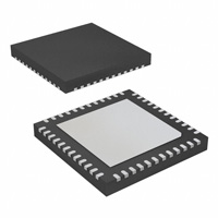
48-Pin PQFN Package
Latch Off After Fault
The TPS2358 dual-slot hot-plug controller provides all
required power interface functions for two
AdvancedMC™
(Advanced
Mezzanine
Card)
modules.
Two fully integrated 3.3-V channels provide inrush
control, current limiting, and overload protection. The
two 12-V channels use an external FET to provide
the same functions, along with ORing control circuits
that allow an external FET to prevent reverse current
flow. External capacitors are used to set fault times.
There is one capacitor for each channel. The 3.3-V
current limits are factory set to AdvancedMC™
compliant levels and the 12-V current limits are
programmed using external sense resistors. The
accurate current sense comparators of the TPS2358
satisfy the narrow ATCA AdvancedMC™ current limit
requirements.
APPLICATIONS
•
•
•
•
•
ATCA Carrier Boards
MicroTCA™ Power Modules
AdvancedMC™ Slots
Systems Using 12 V and 3.3 V
Base Stations
TYPICAL APPLICATION DIAGRAM
EN3A\
EN12A\
ORENA\
CT12A
CT3A
IN3A
VDD3A
VI NT
GND
AGND
EN12B\
E N3 B\
ORENB\
CT3B
CT12B
SETB
IN3B
VDD3B
IN12B
SENPB
12 Vin B
3v3 in
3v3 in
12 Vin A
IN12A
SENPA
SETA
R SET
R SET
R SENSE
R SENSE
TPS2358
SENMB
SENMA
48 PIN QFN
100
100
PASSA
PASSB
BLKA
BLKB
100
OUT12A
OUT3A
1 uF
RS UM 1 2B
RSU M 3 B
SUM3A
PG12 A\
SUM12A
PG3A\
FLT12A\
FLT3A\
AGND
GNDA
GNDB
P G12B\
PG 3B\
FLT12B\
OUT3B
1 uF
SUM3B
OUT12B
FLT3B\
SUM12B
100
COMMON
CIRCUITRY
12 V
3.3 V
AdvancedMC
™
R SUM3A
Optional ORing elements for
Redundant Systems Only
R SUM12A
3.3 V
12 V
AdvancedMC ™
1
2
Please be aware that an important notice concerning availability, standard warranty, and use in critical applications of Texas
Instruments semiconductor products and disclaimers thereto appears at the end of this data sheet.
AdvancedMC, MicroTCA are trademarks of PICMG.
PRODUCTION DATA information is current as of publication date.
Products conform to specifications per the terms of the Texas
Instruments standard warranty. Production processing does not
necessarily include testing of all parameters.
Copyright © 2008–2009, Texas Instruments Incorporated
�TPS2358
SLUS820E – FEBRUARY 2008 – REVISED NOVEMBER 2009
www.ti.com
ORDERING INFORMATION (1)
(1)
(2)
DEVICE
TEMPERATURE
PACKAGE (2)
ORDERING CODE
TPS2358
-40°C to 85°C
QFN48
TPS2358RGZ
Add an R suffix to the device type for tape and reel.
For the most current package and ordering information see the Package Option Addendum at the end of this document or see the TI
Web site at www.ti.com.
ABSOLUTE MAXIMUM RATINGS (1)
Over operating free-air temperature range, all voltages referenced to GND (unless otherwise noted).
PARAMETER
VALUE
Unit
PASSx, BLKx
–0.3 to 30
IN12x, OUT12x, SENPx, SENMx, SETx, EN12x, FLTx, PGx, ORENx
–0.3 to 17
IN3x, OUT3x, EN3x, VDDx, CTx, SUMx
–0.3 to 5
AGND, GNDx
–0.3 to 0.3
FLTx, PGx
5
SUMx
5
VINT
–1 to 1
OUT3x
(1)
V
mA
Internally limited
Stresses beyond those listed under absolute maximum ratings may cause permanent damage to the device. These are stress ratings
only. Functional operation of the device under any conditions beyond those indicated under recommended operating conditions is
neither implied nor guaranteed. Exposure to absolute maximum rated conditions for extended periods of time may affect device
reliability.
ELECTROSTATIC DISCHARGE (ESD) PROTECTION
TEST METHOD
MIN
Human Body Model (HBM)
2
Charged Device Model (CDM)
0.5
UNITS
kV
DISSIPATION RATINGS
PACKAGE
θJA - High-k (°C/W)
QFN48 - RGZ
29.1
RECOMMENDED OPERATING CONDITIONS
over operating free-air temperature range (unless otherwise noted)
PARAMETER
MIN
TYP
MAX
UNITS
VIN12x
12-V input supply
8.5
12
15
VIN3x
3.3-V input supply
3
3.3
4
VVDD3x
3.3-V input supply
3
3.3
4
IOUT3x
3.3-V output current
ISUMx
Summing pin current
165
100
PASSx pin board leakage current
-1
VINT bypass capacitance
TJ
2
1
Operating junction temperature range
–40
Submit Documentation Feedback
1000
1
10
V
mA
μA
250
nF
125
°C
Copyright © 2008–2009, Texas Instruments Incorporated
Product Folder Link(s): TPS2358
�TPS2358
www.ti.com
SLUS820E – FEBRUARY 2008 – REVISED NOVEMBER 2009
ELECTRICAL CHARACTERISTICS
IN3A = IN3B = VDD3A = VDD3B = 3.3 V. IN12A = IN12B = SENPA = SENPB = SENMA = SENMB = SETPA =
SETPB = 12 V. EN12A = EN12B = EN3A = EN3B = ORENA = ORENB = CT12A = CT12B = CT3A = CT3B = AGND =
GNDA = GNDB = 0 V. SUM12A = SUM12B = 6.8 kΩ to ground. SUM3A = SUM3B = 3.3 kΩ to ground. All other pins open.
Over free air temperature operating range and all voltages referenced to AGND, -40°C ≤ TA ≤ 85°C, typical vales at 25°C,
unless otherwise noted.
PARAMETER
CONDITIONS
MIN
TYP
MAX
UNITS
ENABLE Inputs
Threshold voltage, falling
edge
Hysteresis
1.2
1.3
1.4
V
20
50
80
mV
5
8
15
Pullup current
ENx = ORENx = 0 V
Input bias current
EN12x = ORENx = 17 V
6
15
Input bias current
EN3x = 5 V
1
5
3.3-V turn off time
EN3x deasserts to VOUT3x < 1.0 V, COUT = 0 μF
10
12-V turn off time
EN12x deasserts to VOUT12x < 1.0 V, COUT = 0 μF,
QGATE = 35 nF
20
μA
μs
POWER GOOD Outputs
Low voltage
Sinking 2 mA
Leakage current
PGx = 17 V
Threshold voltage
PG12x, falling VOUT12x
PG3x, falling VOUT3x
Hysteresis
0.14
0.25
V
1
μA
10.2
10.5
10.8
2.7
2.8
2.9
PG12x, measured at OUT12x
130
PG3x, measured at OUT3x
Deglitch time
PGx falling
mV
50
50
V
μs
100
150
0.14
0.25
V
1
μA
V
FAULT Outputs
Low voltage
Sinking 2 mA
Leakage current
PGx = 17 V
VINT
Output voltage
0 < IVINT < 50 μA
2
2.3
2.8
–7
–10
–13
7
10
13
Upper threshold voltage
1.3
1.35
1.4
Lower threshold voltage
0.33
0.35
0.37
Fault Timer
Sourcing current
VCTx = 0 V, during fault
Sinking current
VCTx = 2 V
μA
V
12-V Summing Node
Input referred offset
VSENMx = 10.8 – 13.2 V, VSENPx = VSENMx + 50 mV,
measure VSETx – VSENMx
Summing threshold
VPASSx = 15 V
Leakage current
VSETx = VSENMx – 10 mV
–2
0.66
2
0.675
mV
0.69
V
1
μA
52.5
mV
40
μA
100
120
mV
200
300
ns
6
7
V
12-V Current Limit
Current limit threshold
RSUMx = 6.8 kΩ, RSETx = 422 Ω, increase ILOADx and
measure VSENPx – VSENMx when VPASSx = 15 V
Sink current in current
limit
VSUMx = 1 V, VPASSx = 12 V, measure IPASSx
20
Fast trip threshold
Measure VSENPx – VSENMx
80
Fast turn-off delay
20 mV overdrive, CPASSx = 0 pF, tp50-50
Timer start threshold
VPASSx - VINx when timer starts, while VPASSx falling
due to over current
47.5
5
50
Submit Documentation Feedback
Copyright © 2008–2009, Texas Instruments Incorporated
Product Folder Link(s): TPS2358
3
�TPS2358
SLUS820E – FEBRUARY 2008 – REVISED NOVEMBER 2009
www.ti.com
ELECTRICAL CHARACTERISTICS (continued)
IN3A = IN3B = VDD3A = VDD3B = 3.3 V. IN12A = IN12B = SENPA = SENPB = SENMA = SENMB = SETPA =
SETPB = 12 V. EN12A = EN12B = EN3A = EN3B = ORENA = ORENB = CT12A = CT12B = CT3A = CT3B = AGND =
GNDA = GNDB = 0 V. SUM12A = SUM12B = 6.8 kΩ to ground. SUM3A = SUM3B = 3.3 kΩ to ground. All other pins open.
Over free air temperature operating range and all voltages referenced to AGND, -40°C ≤ TA ≤ 85°C, typical vales at 25°C,
unless otherwise noted.
PARAMETER
CONDITIONS
MIN
TYP
MAX
UNITS
12-V UVLO
UVLO rising
IN12x rising
8.1
8.5
8.9
UVLO hysteresis
IN12x falling
0.44
0.5
0.59
V
12-V BLOCKING
Turn-on threshold
Measure VSENPx – VOUTx
5
10
15
Turn-off threshold
Measure VSENPx – VOUTx
–5
–3
0
Turn-off delay
20 mV overdrive, CBLKx = 0 pF, tp50-50
200
300
mV
ns
12-V Gate Drivers ( PASSx, BLKx )
Output voltage
VINx = VOUTx = 10 V
21.5
23
24.5
V
Sourcing current
VIN12x = VOUT12x = 10 V, VPASSx = VBLKx = 17 V
20
30
40
μA
Fast turnoff, VPASSx = VBLKx = 14 V
0.5
1
6
14
25
mA
14
20
26
kΩ
5
10
15
μs
1
μs
0.25
ms
675
695
mV
mΩ
Sinking current
Pulldown resistance
Sustained, VPASSx = VBLKx = 4 – 25 V
In OTSD ( at 150 °C )
Fast turn-off duration
Disable delay
EN12x pin to PASSx and BLKx, tp50-90
Startup time
IN12x rising to PASSx and BLKx sourcing
A
3.3-V Summing Node
Summing threshold
655
3.3-V Current Limit
On resistance
IOUT3x = 150 mA
Current limit
RSUM3x = 3.3 kΩ , VOUT3x = 0 V
Fast trip threshold
Fast turn-off delay
290
500
170
195
225
250
300
400
750
1300
ns
IOUT3x = 400 mA, tp50-50
mA
3.3-V UVLO
UVLO rising
IN3x rising
2.65
2.75
2.85
V
UVLO hysteresis
IN3x falling
200
240
300
mV
3.1
4
2
2.8
Supply Currents (IINx + ISENPx + ISENMx + ISETx + IVDDx)
All channels enabled
IOUT3A = IOUT3B = 0
All channels disabled
mA
Thermal Shutdown
Whole-chip shutdown
temperature
TJ rising, IOUT3A = IOUT3B = 0
140
150
3.3 V channel shutdown
temperature
TJ rising, IOUT3A or IOUT3B in current limit
130
140
Hysteresis
Whole chip or 3.3-V channel
4
Submit Documentation Feedback
°C
10
Copyright © 2008–2009, Texas Instruments Incorporated
Product Folder Link(s): TPS2358
�TPS2358
www.ti.com
SLUS820E – FEBRUARY 2008 – REVISED NOVEMBER 2009
DEVICE INFORMATION
SIGNAL AND PIN NAMING BLOCK
The PICMG™ AdvancedMC™ specification refers to 3.3-V power as management power and refers to 12-V
power as payload power. This datasheet uses a naming convention that reflects the associated voltage (12 V to
3 V) and AdvancedMC™ slot (A or B).
• Signals and pins associated with slot A 12-V payload power end with 12A.
• Signals and pins associated with slot A 3.3-V management power end with 3A.
• Signals and pins associated with slot B 12-V payload power end with 12B.
• Signals and pins associated with slot B 3.3-V management power end with 3B.
Pins and signals unique to 12-V channels have only an A or B suffix.
TPS2358 Block Diagrams
R SENSE
R SET
SENPx
100
SETx
PASSx
SENMx
100
BLKx
OUT12x
pgat\
100 mv
12dis
+
30 uA
30 uA
Q
Pump
+
IN12x
CT12x
10 us
10 us
Vcp
~25 v
Fault
Timer
Vcp
EN12x\
ogat
PG3x\
FLT12x\
675 mV
+
SUM12x
60 m A
6810
OUT12x
10 mv
+
-3 mv
R
Q
S
Q
ogat
100 us
+
pgat\
+
PG12x\
OUT12x
vpg
oren
Figure 1. 12-V Channel Circuitry
Submit Documentation Feedback
Copyright © 2008–2009, Texas Instruments Incorporated
Product Folder Link(s): TPS2358
5
�TPS2358
SLUS820E – FEBRUARY 2008 – REVISED NOVEMBER 2009
www.ti.com
0.1 W
OUT3
IN3
2.8 V
30 uA
+
gat
96 W
en
VDD3
30 mv
+
Q
Pump
30 us
+
PG3x\
vcp
~25 v
Fault
Timer
30 us
FLT3x \
EN3
Control
Logic
SUM3
+
675 mV
3300
60 mA
Figure 2. 3-V Channel Circuitry
IN12A
VINT
en
por
IN12B
PREREG
IN3A
IN3B
POR
Control
Logic
2.2 V
OUT12A
OUT12B
AGND
GNDA
GNDB
OUT3A
OUT3B
Figure 3. Circuitry Common to all Channels
6
Submit Documentation Feedback
Copyright © 2008–2009, Texas Instruments Incorporated
Product Folder Link(s): TPS2358
�TPS2358
www.ti.com
SLUS820E – FEBRUARY 2008 – REVISED NOVEMBER 2009
CT12A
FLT12A
BLKA
OUT12A
GNDA
EN12A
PASSA
EN12B
EN3A
EN3B
VDD3A
IN3A
Control
48
47
46
45
44
43
42
41
40
39
38
37
IN12A
1
36
OUT3A
SENPA
2
35
CT3A
SETA
3
34
FLT3A
SENMA
4
33
PG3A
VINT
5
32
SUM3A
PG12A
6
31
AGND
SUM12A
7
30
VDD3B
ORENA
8
29
SUM3B
GND
9
28
PG3B
GND
10
27
FLT3B
PG12B
11
26
CT3B
SUM12B
12
25
OUT3B
17
18
19
20
21
OUT12B
GNDB
ORENB
PASSB
SENMB
SETB
CT12B
12A, 12B
22
23
24
IN3B
16
IN12B
15
SENPB
14
BLKB
13
FLT12B
48 Pin QFN
3A, 3B
TERMINAL FUNCTIONS
PIN#
NAME
TYPE
DESCRIPTION
1
IN12A
VDD
2
SENPA
I
12A input sense
3
SETA
I
12A current limit set
4
SENMA
I
12A current limit sense
5
VINT
I/O
Bypass capacitor connection point for internal supply
6
PG12A
O
12A power good output, active low, asserts when OUT12A > VPG12A
7
SUM12A
I/O
12A summing node
8
ORENA
I
9
GND
GND
Connect pin to ground
10
GND
GND
Connect pin to ground
12A input
12A blocking transistor enable, active low
11
PG12B
O
12B power good output, active low, asserts when OUT12B > VPG12B
12
SUM12B
I/O
12B summing node
Submit Documentation Feedback
Copyright © 2008–2009, Texas Instruments Incorporated
Product Folder Link(s): TPS2358
7
�TPS2358
SLUS820E – FEBRUARY 2008 – REVISED NOVEMBER 2009
www.ti.com
TERMINAL FUNCTIONS (continued)
PIN#
8
NAME
TYPE
DESCRIPTION
13
CT12B
I/O
12B fault timing capacitor
14
FLT12B
O
12B fault output, active low, asserted when 12B fault timer runs out
15
BLKB
O
12B blocking transistor gate drive
16
OUT12B
I/O
12B output
17
GNDB
GND
18
ORENB
I
12B blocking transistor enable, active low
19
PASSB
O
12B pass transistor gate drive
20
SENMB
I
12B current limit sense
21
SETB
I
12B current limit set
22
SENPB
I
12B input sense
23
IN12B
VDD
12B input
24
IN3B
VDD
3B input
25
OUT3B
I/O
3B output
26
CT3B
I/O
3B fault timing capacitor
27
FLT3B
O
3B fault output, active low, asserted when 3B fault timer runs out
28
PG3B
O
3B power good output, active low, asserts when OUT3B > 2.8 V
29
SUM3B
I/O
3B summing node
30
VDD3B
VDD
3B charge pump input
31
AGND
GND
Analog ground
32
SUM3A
I/O
3A summing node
33
PG3A
O
3A power good output, active low, asserts when OUT3A > 2.8 V
34
FLT3A
O
3A fault output, active low, asserted when 3A fault timer runs out
35
CT3A
I/O
3A fault timing capacitor
36
OUT3A
I/O
3A output
37
IN3A
VDD
3A input
38
VDD3A
VDD
3A charge pump input
39
EN3B
I
3B enable, (default active low)
40
EN3A
I
3A enable, (default active low)
41
EN12B
I
12B enable, (default active low)
42
PASSA
O
12A pass transistor gate drive
43
EN12A
I
12A enable, (default active low)
44
GNDA
GND
45
OUT12A
I/O
12A output
12B power ground
12A power ground
46
BLKA
O
12A blocking transistor gate drive
47
FLT12A
I/O
12A fault output, active low, asserted when 12A fault timer runs out
48
CT12A
I/O
12A fault timing capacitor
Submit Documentation Feedback
Copyright © 2008–2009, Texas Instruments Incorporated
Product Folder Link(s): TPS2358
�TPS2358
www.ti.com
SLUS820E – FEBRUARY 2008 – REVISED NOVEMBER 2009
DEVICE INFORMATION
DETAILED PIN DESCRIPTION
AGND Ground pin for the analog circuitry inside the TPS2358.
BLKx Gate drive pin for the 12x channel BLK FET. This pin sources 30 μA to turn the FET on. An internal clamp
prevents this pin from rising more than 14.5 V above OUT12x. Setting the ORENx pin high holds the BLKx pin
low.
CTx A capacitor from CTx to GND sets the time the channel can remain in current limit before it shuts down and
declares a fault. Current limit causes this pin to source 10 μA into the external capacitor (CT). When VCTx
reaches 1.35 V, the TPS2358 shuts the channel off by pulling the PASSx pin low and declares an over-current
fault by pulling the FLTx pin low.
EN12x Active low enable input. Pulling this pin high (or allowing it to float high) turns off channel 12x by pulling
both BLKx and PASSx low. An internal 200-kΩ resistor pulls this pin up to VINT when disconnected.
EN3x Active low enable input. Pulling this pin high (or allowing it to float high) turns off channel 3x by pulling the
gate of the internal pass FET to GND. An internal 200-kΩ resistor pulls this pin up to VINT when disconnected.
FLTx Active low open-drain output indicating that channel x has remained in current limit long enough to time out
the fault timer and shut the channel down.
IN12x Supply pin for channel 12x internal circuitry.
IN3x Supply pin for channel 3x internal pass FET.
ORENx Active low input. Pulling this pin low allows the 12x channel ORing function to operate normally. Pulling
this pin high (or allowing it to float high) disables the ORing function by pulling the BLKx pin low. An internal
200-kΩ resistor pulls this pin up to VINT when disconnected.
OUT12x Senses the output voltage of the channel 12x path. OUT12x is the return node for the BLKx pin clamp.
This pin will source ~30 µA when the BLK FET is fully enhanced.
OUT3x Output of the channel 3x internal pass FET.
PASSx Gate drive pin for the 12x channel pass FET. This pin sources 30 μA to turn the FET on. An internal
clamp prevents this pin from rising more than 14.5 V above IN12x.
PGx Active low open-drain output indicating that channel x output voltage is above the PG threshold, which
nominally equals 2.85 V for the 3x channels and 10.5 V for the 12x channels.
SENMx Senses the voltage on the low side of the channel 12x current sense resistor.
SENPx Senses the voltage on the high side of the channel 12x current sense resistor.
SETx A resistor connected from this pin to SENPx sets the current limit level in conjunction with the current
sense resistor and the resistor connected to the SUM12x pin, as described in 12-V thresholds – setting current
limit and fast over current trip section.
SUMx A resistor connected from this pin to ground forms part of the channel x current limit. As the current
delivered to the load increases, so does the voltage on this pin. When the voltage on this pin reaches a threshold
of 675 mV, the current limit amplifier acts to prevent the current from further increasing.
VDD3x Supply pin for channel3x internal circuitry.
VINT This pin connects to the internal 2.35-V rail. A 0.1-μF capacitor must be connected from this pin to ground.
Do not connect other external circuitry to this pin.
Submit Documentation Feedback
Copyright © 2008–2009, Texas Instruments Incorporated
Product Folder Link(s): TPS2358
9
�TPS2358
SLUS820E – FEBRUARY 2008 – REVISED NOVEMBER 2009
www.ti.com
TYPICAL CHARACTERISTICS
3VIDD
vs
TEMPERATURE
12-V CURRENT LIMIT THRESHOLD
51.0
2.45
2.40
50.8
2.35
mV
IDD - mA
50.6
2.30
50.4
2.25
2.20
50.2
2.15
50.0
-50
2.10
-50
0
50
100
0
50
100
150
TJ - Temperature - °C
150
TJ - Temperature
Figure 4.
Figure 5.
3-V IDD
vs
TEMPERATURE
12-V CHANNEL ORING TURN-OFF THRESHOLD
0.0
0.26
-1.0
0.25
-2.0
mV
IDD - mA
0.24
0.23
-3.0
0.22
-4.0
0.21
-5.0
0.20
-50
-50
0
50
100
150
0
50
100
150
TJ - Temperature - °C
TJ - Temperature - °C
Figure 6.
10
Figure 7.
Submit Documentation Feedback
Copyright © 2008–2009, Texas Instruments Incorporated
Product Folder Link(s): TPS2358
�TPS2358
www.ti.com
SLUS820E – FEBRUARY 2008 – REVISED NOVEMBER 2009
TYPICAL CHARACTERISTICS (continued)
12-V CURRENT (mA)
vs
TEMPERATURE
12-V CHANNEL ORING TURN-ON THRESHOLD
12.0
2.4
11.5
11.0
2.3
mV
Current - mA
10.5
10.0
2.2
6
9.5
9.0
2.1
8.5
8.0
2.0
-50
-50
0
50
100
150
TJ - Temperature - °C
Figure 8.
0
50
100
150
TJ - Temperature - °C
Figure 9.
Figure 10. OUT3A Startup Into 22-Ω ( 150 mA ) 150-μF Load
Submit Documentation Feedback
Copyright © 2008–2009, Texas Instruments Incorporated
Product Folder Link(s): TPS2358
11
�TPS2358
SLUS820E – FEBRUARY 2008 – REVISED NOVEMBER 2009
www.ti.com
TYPICAL CHARACTERISTICS (continued)
Figure 11. OUT3A Load Stepped from 165 mA to 240 mA
Figure 12. OUT3A Short Circuit under Full Load (165 mA) Zoom View
12
Submit Documentation Feedback
Copyright © 2008–2009, Texas Instruments Incorporated
Product Folder Link(s): TPS2358
�TPS2358
www.ti.com
SLUS820E – FEBRUARY 2008 – REVISED NOVEMBER 2009
TYPICAL CHARACTERISTICS (continued)
Figure 13. OUT3A Short Circuit Under Full Load (165 mA) Wide View
Figure 14. OUT3A Startup Into Short Circuit
Submit Documentation Feedback
Copyright © 2008–2009, Texas Instruments Incorporated
Product Folder Link(s): TPS2358
13
�TPS2358
SLUS820E – FEBRUARY 2008 – REVISED NOVEMBER 2009
www.ti.com
TYPICAL CHARACTERISTICS (continued)
Figure 15. OUT12A Startup Into 500-Ω, 830-μF Load
Figure 16. OUT12A Startup Into 80-Watt, 830-μF Load
14
Submit Documentation Feedback
Copyright © 2008–2009, Texas Instruments Incorporated
Product Folder Link(s): TPS2358
�TPS2358
www.ti.com
SLUS820E – FEBRUARY 2008 – REVISED NOVEMBER 2009
TYPICAL CHARACTERISTICS (continued)
Figure 17. OUT12A Short Circuit Under Full Load (6.7 A) Wide View
Figure 18. OUT12A Short Circuit Under Full Load (6.7 A) Zoom View
Submit Documentation Feedback
Copyright © 2008–2009, Texas Instruments Incorporated
Product Folder Link(s): TPS2358
15
�TPS2358
SLUS820E – FEBRUARY 2008 – REVISED NOVEMBER 2009
www.ti.com
TYPICAL CHARACTERISTICS (continued)
Figure 19. OUT12A Startup Into Short Circuit
Figure 20. OUT12A Overloaded While Supplying 6.7 A
16
Submit Documentation Feedback
Copyright © 2008–2009, Texas Instruments Incorporated
Product Folder Link(s): TPS2358
�TPS2358
www.ti.com
SLUS820E – FEBRUARY 2008 – REVISED NOVEMBER 2009
REFERENCE INFORMATION
The TPS2358 has been designed to simplify compliance with the PICMG-AMC.R2.0 and PICMG-MTCA.0
specifications. These specifications were developed by the PCI Industrial Computer Manufacturers Group
(PICMG). These two specifications are derivations of the PICMG-ATCA (Advanced Telecommunication
Computing Architecture) specification originally released in December, 2002.
PICMG-AMC Highlights
•
•
•
•
•
•
•
•
•
AMC – Advanced Mezzanine Cards
Designed to Plug Into ATCA Carrier Boards
AdvancedMC™ Focuses on Low Cost
1 to 8 AdvancedMC™ per ATCA Carrier Board
3.3-V Management Power (maximum current draw of 150 mA)
12-V Payload Power – (converted to required voltages on AMC)
Maximum 80-W Dissipation per AdvancedMC™
Hotswap and Current Limiting Must be Present on Carrier Board
For Details,See www.picmg.org/v2internal/AdvancedMC.htm
PICMG-MTCA Highlights
•
•
•
•
•
•
•
MTCA - MicroTelecommunications Computing Architecture
Architecture for Using AMCs Without an ATCA Carrier Board
Up to 12 AMCs Per System, Plus Two MCHs and Two CUs
Focuses on Low Cost
All Functions of ATCA Carrier Board Must be Provided
MicroTCA is Also Known as MTCA, mTCA, or uTCA
For Details, See www.picmg.org/v2internal/microTCA.htm
Submit Documentation Feedback
Copyright © 2008–2009, Texas Instruments Incorporated
Product Folder Link(s): TPS2358
17
�TPS2358
SLUS820E – FEBRUARY 2008 – REVISED NOVEMBER 2009
www.ti.com
SYSTEM OPERATION
Introduction
The TPS2358 controls two 12-V power paths and two 3.3-V power paths. Each power path can draw from a
single common supply, or from two independent supplies. The TPS2358 is in a 48-pin QFN package. The
following sections describe the main functions of the TPS2358 and provide guidance for designing systems
around this device.
Control Logic and Power-On Reset
The TPS2358's circuitry draws power from an internal bus fed by a preregulator. A capacitor attached to the
VINT pin provides decoupling and output filtering for this preregulator. It can draw power from any of four inputs
(IN12A, IN12B, IN3A, or IN3B) or from any of four outputs (OUT12A, OUT12B, OUT3A, or OUT3B). This feature
allows the internal circuitry to function regardless of which channels receive power, or from what source. The four
external FET drive pins (PASSA, PASSB, BLKA, and BLKB) are held low during startup to ensure that the two
12-V channels remain off. The internal 3.3-V channels are also held off. When the voltage on the internal VINT
rail exceeds approximately 1 V, the power-on reset circuit initializes the TPS2358.
Enable Functions
The TPS2358 provides three external enable pins for each of its two AdvancedMC™ slots. Pulling the EN3x low
turns on the 3x channel. Pulling the EN12x pin turns on the 12x channel. If the EN12x pin goes high, the
TPS2358 pulls both the PASSx and BLKx pins to ground. Pulling the ORENx pin low turns on the reverse
blocking circuitry in the 12x channel. If the ORENx pin goes high, then the BLKx pin remains low. Each of the six
enable pins has an internal 200-kΩ pullup resistor to VINT. To comply with AdvancedMC™ requirements, the
12-V Channels will not enable unless the associated 3.3 channel PG is asserted.
Power Good (PG) Outputs
The TPS2358 provides four active-low open-drain outputs that monitor the status of the four output voltage rails.
The power good output for each channel pulls low whenever the voltage on its OUTx pin exceeds the PG
threshold. The 3.3-V channels have nominal thresholds of 2.85 V and the 12-V channels have nominal
thresholds of 10.5 V.
Fault (FLT) Outputs
The TPS2358 provides four active-low, open-drain fault outputs, one for each channel. A fault output pulls low
when the channel has remained in current limit long enough to run out the fault timer. A channel experiencing a
fault condition automatically shuts down. To clear the fault and re-enable the channel, turn the channel off and
back on using the appropriate ENx pin.
Current Limit and Fast Trip Thresholds
All four channels monitor current by sensing the voltage across a resistor. The 3.3-V channels use internal sense
resistors with a nominal value of 290 mΩ. The 12-V channels use external sense resistors that typically lie in the
range of 4 - 10 mΩ. Each channel features two distinct thresholds: a current limit threshold and a fast trip
threshold.
The current limit threshold sets the regulation point of a feedback loop. If the current flowing through the channel
exceeds the current limit threshold, then this feedback loop reduces the gate-to-source voltage imposed on the
pass FET. This causes the current flowing through the channel to settle to the value determined by the current
limit threshold. For example, when a module first powers up, it draws an inrush current to charge its load
capacitance. The current limit feedback loop ensures that this inrush current does not exceed the current limit
threshold.
The current limit feedback loop has a finite response time. Serious faults such as shorted loads require a faster
response in order to prevent damage to the pass FETs or voltage sags on the supply rails. A comparator
monitors the current flowing through the sense resistor, and if it ever exceeds the fast trip threshold, then it
immediately shuts off the channel. The channel turns back on slowly, allowing the current limit feedback loop
time to respond. One normally sets the fast trip threshold some 2 to 5 times higher than the current limit.
18
Submit Documentation Feedback
Copyright © 2008–2009, Texas Instruments Incorporated
Product Folder Link(s): TPS2358
�TPS2358
www.ti.com
SLUS820E – FEBRUARY 2008 – REVISED NOVEMBER 2009
3.3-V Current Limiting
The 3.3-V management power channels include internal pass FETs and current sense resistors. The
on-resistance of a management channel - including pass FET, sense resistor, metallization resistance, and bond
wires - typically equals 290 mΩ and never exceeds 500 mΩ. The AdvancedMC™ specification allows a total of 1
Ω between the power source and the load. The TPS2358 never consumes more than half of this budget.
3.3-V Fast Trip Function
The 3.3-V fast trip function protects the channel against short-circuit events. If the current through the channel
exceeds a nominal value of 300 mA, then the TPS2358 immediately disables the internal pass transistor and
then allows it to slowly turn back on into current limiting.
3.3-V Current Limit Function
The 3.3-V current limit function internally limits the current to comply with the AdvancedMC™ and MicroTCA™
specifications. External resistor RSUM3x allows the user to adjust the current limit threshold. The nominal current
limit threshold ILIMIT equals:
I LIMIT =
650V
RSUM 3 x
(1)
A 3320-Ω resistor gives a nominal current limit of ILIMIT = 195 mA which complies with AdvancedMC™ and
MicroTCA™ specifications. This resistance corresponds to an EIA 1% value. Alternatively, a 3.3-kΩ resistor will
also suffice. Whenever a 3.3-V channel enters current limit, its fault timer begins to operate (see Fault Timer
Programming section).
3.3-V Over-Temperature Shutdown
The 3.3-V over-temperature shutdown trips if a 3.3-V channel remains in current limit so long that the die
temperature exceeds approximately 140°C. When this occurs, any 3.3-V channel operating in current limit turns
off until the chip cools by approximately 10°C. This feature prevents a prolonged fault on one 3.3-V channel from
disabling the other 3.3-V channel, or disabling either of the 12-V channels.
Submit Documentation Feedback
Copyright © 2008–2009, Texas Instruments Incorporated
Product Folder Link(s): TPS2358
19
�TPS2358
SLUS820E – FEBRUARY 2008 – REVISED NOVEMBER 2009
www.ti.com
12-V Fast Trip and Current Limiting
Figure 21 shows a simplified block diagram of the circuitry associated with the fast trip and current limit circuitry
within a 12-V channel. Each 12-V channel requires an external N-channel pass FET and three external resistors.
These resistors allow the user to independently set the fast trip threshold and the current limit threshold, as
described below.
12-V Fast Trip Function
The 12-V fast trip function is designed to protect the channel against short-circuit events. If the voltage across
RSENSE exceeds a nominal threshold of 100 mV, the device immediately disables the pass transistor and
declares a fault condition. The nominal fast current limit equals:
I FT =
100mV
RS
(2)
12-V Current Limit Function
The 12-V current limit function regulates the PASSx pin voltage to prevent the current through the channel from
exceeding ILIMIT. The current limit circuitry includes two amplifiers, A1 and A2, as shown in Figure 21. Amplifier A1
forces the voltage across external resistor RSET to equal the voltage across external resistor RSENSE. The current
that flows through RSET also flows through external resistor RSUM, generating a voltage on the 12SUMx pin equal
to:
æR
R
V12 SUMx = ç SENSE SUM
RSET
è
ö
÷ I SENSE
ø
(3)
Amplifier A2 senses the voltage on the 12SUMx pin. As long as this voltage is less than the reference voltage on
its positive input (nominally 0.675 V), the amplifier sources current to PASSx. When the voltage on the 12SUMx
pin exceeds the reference voltage, amplifier A2 begins to sink current from PASSx. The gate-to-source voltage of
pass FET MPASS drops until the the voltages on the two inputs of amplifier A2 balance. The current flowing
through the channel then nominally equals:
æ
ö
RSET
I LIMIT = ç
÷ × 0.675V
è RSUM RSENSE ø
20
(4)
Submit Documentation Feedback
Copyright © 2008–2009, Texas Instruments Incorporated
Product Folder Link(s): TPS2358
�TPS2358
www.ti.com
SLUS820E – FEBRUARY 2008 – REVISED NOVEMBER 2009
The recommended value of RSUM is 6810 Ω. This resistor should never equal less than 675 Ω to prevent
excessive currents from flowing through the internal circuitry. Using the recommended values of RSENSE = 5 mΩ
and RSUM = 6810 Ω gives:
I LIMIT = ( 0.0198 A / W ) × RSET
(5)
A system capable of powering an 80-Watt AdvancedMC™ module consumes a maximum of 8.25 A according to
MicroTCA™ specifications. The above equation suggests RSET = 417 Ω. The nearest 1% EIA value equals 422
Ω. The selection of RSET for MicroTCA™ power modules is described in the Redundant vs. Non-Redundant
Inrush Current Limiting section.
R SENSE
IN12x
R SET
SETx
100
PASSx
SENMx
SENPx
+
100 mV
Fast Trip
Comparator
+
A1
Current
Limit Amp
675 mV
60 mA
30 mA
+
A2
SUM12x
R SUM
Figure 21. 12-V Channel Threshold Circuitry
Fault Timer Programming
The fault timers of the four channels in a TPS2358 use identical internal circuitry. Each channel requires an
external capacitor CT connected between the CTx pin and ground. Whenever the gate drive is less than 6 V the
timer will be charging CT. When a channel goes into current limit, the TPS2358 injects 10 μA into the external
capacitor. If the channel remains in current limit long enough for the voltage on the CTx pin to reach 1.35 V, then
the TPS2358 shuts the channel down and pulls the FLTx pin low to declare a fault. If the channel does not
remain in current limit long enough to trip the timer, then the CTx capacitor is discharged through an internal
200-Ω pulldown resistor. The nominal fault time tf equals:
tf =
1.35V
CT
10 m A
(6)
-6
CT = 7.4 ´10 ´ TF
(7)
The user should select capacitors that provide the shortest fault times sufficient to allow down-stream loads and
bulk capacitors to charge. Shorter fault times reduce the stresses imposed on the pass FETs under fault
conditions. This consideration may allow the use of smaller and less expensive FETs for the 12-V channels.
Submit Documentation Feedback
Copyright © 2008–2009, Texas Instruments Incorporated
Product Folder Link(s): TPS2358
21
�TPS2358
SLUS820E – FEBRUARY 2008 – REVISED NOVEMBER 2009
www.ti.com
Multiswap Operation in Redundant Systems
TheTPS2358 features an additional mode of operation called Multiswap redundancy. This technique does not
require a microcontroller, making it simpler and faster than the redundancy schemes described in the
MicroTCA™ standard. Multiswap is especially attractive for AdvancedMC™ applications that require redundancy
but need not comply with the MicroTCA™ power module standard.
In order to implement Multiswap redundancy, connect the SUM pins of the redundant supplies together and tie a
single RSUM resistor from this node to ground. The current limit thresholds now apply to the sum of the currents
delivered by the redundant supplies. When implementing multiswap redundancy on 12-V channels, all of the
channels must use the same values of resistors for RSENSE and RSET.
Figure 22 compares the redundancy technique advocated by the MicroTCA™ specification to multiswap
redundancy. MicroTCA™ redundancy independently limits the current delivered by each power source. The
current drawn by the load cannot exceed the sum of the current limits of the individual power sources. Multiswap
redundancy limits the current drawn by the load to a fixed value regardless of the number of operational power
sources. Removing or inserting power sources within a multiswap system does not affect the current limit seen
by the load.
MicroTCA TM Redundancy
Power Source 2
mC
TPS2358
SUM3x
SUM12x
TPS2358
SUM3x
SUM12x
RSUM12x
mC
SUM12x
RSUM12x
SUM3x
RSUM3x
RSUM12x
SUM12x
TPS2358
Power Source 2
SUM3x
RSUM3x
TPS2358
Power Source 1
Backplane
RSUM3x
Power Source 1
Multiswap Redundancy
Backplane
Figure 22. MicroTCA™ Redundancy vs. Multiswap Redundancy
22
Submit Documentation Feedback
Copyright © 2008–2009, Texas Instruments Incorporated
Product Folder Link(s): TPS2358
�TPS2358
www.ti.com
SLUS820E – FEBRUARY 2008 – REVISED NOVEMBER 2009
12-V Inrush Slew Rate Control
As normally configured, the turn-on slew rate of the 12-V channel output voltage VOUT equals:
dVout I src
@
dt
Cg
(8)
where ISRC equals the current sourced by the PASSx pin (nominally 30 μA) and Cg equals the effective gate
capacitance. For purposes of this computation, one can assume that the effective gate capacitance
approximately equals the reverse transfer capacitance, CRSS. To reduce the slew rate, increase Cg by connecting
additional capacitance from PASSx to ground. Place a resistor of at least 1000 Ω in series with the additional
capacitance to prevent it from interfering with the fast turn off of the FET. Due to the current limit function at start
up it is unlikely that slew rate control will be required.
R SENSE
IN12
R > 1k W
C
100 W
PASS
Figure 23. RC Slew Rate Control
12-V ORing Operation for Redundant Systems
The 12-V channels use external pass FETs to provide reverse blocking. The TPS2358 pulls the BLKx pin high
when the input-to-output differential voltage VIN12x-OUT12x exceeds a nominal value of 10 mV, and it pulls the
pin low when this differential falls below a nominal value of -3 mV. These thresholds provide a nominal 13 mV of
hysteresis to help prevent false triggering (Figure 24).
V GATE
The source of the blocking FET connects to the source of the pass FET, and the drain of the blocking FET
connects to the load. This orients the body diode of the blocking FET such that it conducts forward current and
blocks reverse current. The body diode of the blocking FET does not normally conduct current because the FET
turns on when the voltage differential across it exceeds 10 mV.
10 mV
Gnd
- 3 mV
25 V
VOR
Figure 24. ORing Thresholds
Submit Documentation Feedback
Copyright © 2008–2009, Texas Instruments Incorporated
Product Folder Link(s): TPS2358
23
�TPS2358
SLUS820E – FEBRUARY 2008 – REVISED NOVEMBER 2009
www.ti.com
Using the TPS2358 to Control Two AdvancedMC™ Slots
The TPS2358 has been designed for use on ATCA Carrier boards with a minimum number of external
components. Carrier boards do not usually have redundant 3.3-V or 12-V supplies, so it is not necessary to
provide ORing functions in the power supply feeds. Consequently, the external 12-V ORing FETs have been
omitted and the BLKx pins are left unconnected.
CSD16406Q3
12 V
MBRM120
0.005 W
0.01 mF
0.01 mF
1 mF
499 W
100 W
AMC A
NC
SENPA
SENMA PASSA BLKA OUT12A
SETA
IN12A
EN12A
EN3A
ORENA
From
IPMC
0.033 mF
0.033 mF
0.01 mF
3.3 V
4700 x 4
CT12A
IN3A
PG12A
FLT12A
PG3A
FLT3A
VDD3A
SUM12A
CT3A
0.01 mF
0.01 mF
3.3 V
3.3 V
OUT3A
12 VIN
SUM3A
VINT
TPS2358
AGND
GND
48 PIN QFN
To IPMC
and/or
LED’s
6810 W
3320 W
GND
GND
GND
3.3 V
From
IPMC
0.033 mF
0.033 mF
EN12B
EN3B
ORENB
4700 x 4
CT3B
IN3B
VDD3B
0.01 mF
SUM12B
SUM3B
0.01 mF
6810 W
3320 W
3.3 V
OUT3B
IN12B
SENPB
To IPMC
and/or
LED’s
PG12B
FLT12B
PG3B
FLT3B
CT12B
SETB
SENMB PASSB
0.01 mF
OUT12B
BLKB
499 W
MBRM120
AMC B
100 W
0.01 mF
0.005 W
1 mF
12 V
CSD16406Q3
Figure 25. Block Diagram of TPS2358 In a Non-Redundant System
24
Submit Documentation Feedback
Copyright © 2008–2009, Texas Instruments Incorporated
Product Folder Link(s): TPS2358
�TPS2358
www.ti.com
SLUS820E – FEBRUARY 2008 – REVISED NOVEMBER 2009
Layout Considerations
TPS2358 applications require layout attention to ensure proper performance and minimize susceptibility to
transients and noise. In general, all runs should be as short as possible but the list below deserves first
consideration.
1. Decoupling capacitors on IN12A, IN12B, IN3A, and IN3B should have minimal length to the pin and to GND.
2. SENMx and SENPx runs must be short and run side by side to maximize common mode rejection. Kelvin
connections should be used at the points of contact with RSENSE (Figure 26).
3. SETx runs need to be short on both sides of RSET.
4. These runs should be as short as possible and sized to carry at least 20 Amps, more if possible.
(a) Runs on both side of RSENSE.
(b) Runs from the drains and sources of the external FETs.
5. Runs from the BLK FETs to OUT12x should be as short as possible.
6. Runs connecting to IN3x and OUT3x should be sized for 1 Amp or more.
7. Connections to GND and SUMx pins should be minimized after the runs above have been placed.
8. The device dissipates low to average power so soldering the powerpad to the board is not a requirement.
However, doing so will improve thermal performance and reduce susceptibility to noise.
LOAD CURRENT
PATH
TPS2358
RSET
SET
SENP
SET
SENM
SENP
RSET
SENSE
RESISTOR
SENM
LOAD CURRENT
PATH
TPS2358
(a)
(b)
Figure 26. Recommended RSENSE Layout
NOTE
Additional details omitted for clarity.
Submit Documentation Feedback
Copyright © 2008–2009, Texas Instruments Incorporated
Product Folder Link(s): TPS2358
25
�TPS2358
SLUS820E – FEBRUARY 2008 – REVISED NOVEMBER 2009
www.ti.com
Transient Protection
TPS2358 devices in deployed systems are not likely to have long, inductive feeds or long load wires. However, it
is always advised that an analysis be performed to determine the need for transient protection. When the
TPS2358 interrupts current flow, any inductance on the input will tend to cause a positive voltage spike on the
input, and any inductance on the output will tend to cause a negative voltage spike on the output. The following
equations allow the designer to make a reasonably accurate prediction of the voltage spike due to interruptions in
current.
VSPIKE = VNOM + I LOAD L
C
(9)
where:
• VNOM = nominal voltage at terminal being analyzed
• L = combined inductance of feed and RTN lines
• C = capacitance at point of disconnect
• ILOAD = current through terminal at TDISCONNECT
•
é
ù
æ 4 ´ length ö
LSTRAIGHTWIRE ~ ê 0.2 ´ length ´ ln ç
÷ - 0.75 ú nH
è diameter ø
ë
û
This equation can be used to calculate the capacitance required to limit the voltage spike to a desired level
above the nominal voltage:
C=
26
LI 2
(VSPIKE - VNOM )2
(10)
Submit Documentation Feedback
Copyright © 2008–2009, Texas Instruments Incorporated
Product Folder Link(s): TPS2358
�TPS2358
www.ti.com
SLUS820E – FEBRUARY 2008 – REVISED NOVEMBER 2009
Output Protection Considerations for MicroTCA Power Systems
MicroTCA Power systems have particular transient protection requirements because of the basic power
architecture. Traditional protection methods must be adjusted to accommodate these systems where the supplies
are OR’ed together after the inrush control and current limit circuits. However, minor changes to some standard
techniques will yield very good results.
Unlike systems which have hotswap/inrush control at the load, uTCA power modules and their hot swap circuitry
are often a significant distance (up to 1 m of trace length, two way ) from the load module. Even with the best
designed backplanes this distance results in stray inductance which will store energy while current is being
delivered to the load. The inductive energy can cause large negative voltage spikes at the power module output
when the current is switched off under load. The spikes become especially severe when the channel shuts off
due to a short circuit, which drives the current well above normal levels at shut off.
The lowest voltage allowed on the device pins is -0.3 V. If a transient makes a pin more negative than -0.3 V the
internal ESD diode attached to the pin will become forward biased and current will be conducted across the
substrate to the ground pins. This current may disrupt normal operation or, if large enough, damage the silicon.
Typical protection solutions involve capacitors, TVSs ( Transient Voltage Suppressors ) and/or a Schottky diode
to absorb the energy which appears at the power module output in the form of a large negative voltage spike.
The Risk With Output Capacitors
Putting transient filter capacitors at the output of a uTCA power module can cause nuisance trips when that
power module is plugged into an active bus. If there is no series resistance with the capacitor and the bus is low
impedance an inrush surge can cause the active supply to “detect” a short circuit and shut down. One possible
solution is to put a few Ohms of resistance in series with the cap to limit inrush below the fast trip level. A better
solution is to put a Schottky diode across the output to clamp the transient energy and shunt it to ground as
shown in Figure 27. Although the Schottky diode will absorb most of the energy, the extremely fast di/dt at
shutoff allows some of the leading edge energy to couple through the parasitic capacitances of the hotswap FET
and the ORing FET, ( CDS, CGS, CGD ) and into the BLK and GATE pins. Protection for these pins is provided by
100-Ω GATE resistors which have little effect on normal operation but provide good isolation during transient
events.
Simplified PASS FET
Simplified BLK FET
CDS
CDS
OUT12
LP
RP
L P +L EMI_FILTER
IN12
CGD
C GS
100
PASS
ESD
Diode
E=LI 2 /2
1k
100
SENP
C GD
CGS
BLK
ESD
Diode
OUT12
ESD
Diode
ESD
Diode
RP
LP
LP
E=LI 2 /2
TPS2358
POWER MODULE
BACKPLANE
AMC
Figure 27. Figure 32 Parasitic Inductance and Transient Protection
Output Bleed Down Resistance
When the TPS2358 commands the 12-V channel off there is a small leakage current sourced by the OUT12 pin.
If this leakage is ignored it can eventually charge any external capacitance to approximately 6 V. In some
systems this may be acceptable but, if not, the leakage can be bled to GND by a 1-kΩ resistor from OUT12 to
GND will suffice. Maximum leakage is around 23 µA and can be modeled as a 6-V source in series with a
280-kΩ resistor.
Submit Documentation Feedback
Copyright © 2008–2009, Texas Instruments Incorporated
Product Folder Link(s): TPS2358
27
�PACKAGE OPTION ADDENDUM
www.ti.com
10-Dec-2020
PACKAGING INFORMATION
Orderable Device
Status
(1)
Package Type Package Pins Package
Drawing
Qty
Eco Plan
(2)
Lead finish/
Ball material
MSL Peak Temp
Op Temp (°C)
Device Marking
(3)
(4/5)
(6)
TPS2358RGZR
ACTIVE
VQFN
RGZ
48
2500
RoHS & Green
NIPDAU
Level-3-260C-168 HR
-40 to 85
TPS2358
TPS2358RGZT
ACTIVE
VQFN
RGZ
48
250
RoHS & Green
NIPDAU
Level-3-260C-168 HR
-40 to 85
TPS2358
(1)
The marketing status values are defined as follows:
ACTIVE: Product device recommended for new designs.
LIFEBUY: TI has announced that the device will be discontinued, and a lifetime-buy period is in effect.
NRND: Not recommended for new designs. Device is in production to support existing customers, but TI does not recommend using this part in a new design.
PREVIEW: Device has been announced but is not in production. Samples may or may not be available.
OBSOLETE: TI has discontinued the production of the device.
(2)
RoHS: TI defines "RoHS" to mean semiconductor products that are compliant with the current EU RoHS requirements for all 10 RoHS substances, including the requirement that RoHS substance
do not exceed 0.1% by weight in homogeneous materials. Where designed to be soldered at high temperatures, "RoHS" products are suitable for use in specified lead-free processes. TI may
reference these types of products as "Pb-Free".
RoHS Exempt: TI defines "RoHS Exempt" to mean products that contain lead but are compliant with EU RoHS pursuant to a specific EU RoHS exemption.
Green: TI defines "Green" to mean the content of Chlorine (Cl) and Bromine (Br) based flame retardants meet JS709B low halogen requirements of