TPS2363
www.ti.com
SLUS680B – JANUARY 2006 – REVISED JANUARY 2010
PCIExpress Server Dual Slot Hot Plug Controller
Check for Samples: TPS2363
FEATURES
DESCRIPTION
•
•
•
•
•
•
•
•
•
The TPS2363 is a dual-slot PCIExpress hot plug
controller with SMBus control and monitoring
functions. There are sense resistor programmable
current limits for the 3.3-V and 12-V supply.
1
2
Meets PCIExpress™ Hot Plug Requirements
Programmable 12-V Current Limit
Inrush Current Limiting
SMBus
Direct Mode
VAUX Internal FET
General Purpose Inputs
Available in a 48-Pin TQFP Package
MIC2592B Pin Compatible with Additional
Features
The TPS2363 has one internal FET channel for AUX
and two external FET channels for 3.3-V and 12-V
per slot.
The TPS2363PFB is in 48-pin TQFP package.
Application Diagram
12 V
+ 12 V AOUT
By 1 50 mΩ
By 4/8 20 mΩ
By 16 10 mΩ
13 mΩ
3.3 V AOUT
3.3 V
AUXINA
Interrupt
FAULTB
PGOODB
OUT33 B
G33B
SL33B
OUT12 B
SH33B
G12B
SL12B
PGOODA
FAULTA
FILTER A
RFILTERA/B
FILTER B
TQFP
GPIB1
GPIB2
AUXHIB
ONB
AUX ENB
FORCEONB
SH12B
O UT33A
G33A
VAUXA
INT
PFB 48 PIN
A2
A1
A0
SDA
SCL
AUXINB
SL33A
Direct mode
Control B
SH33A
Switches B
AUXHIA
FORCEONA
AUXENA
ONA
GPIA1
GPIA2
OU T12A
SMBus
G12A
Switches A
SL12A
Direct mode
Control A
SH12A
AUXINA
VAUXB
AUXINB
12 V
12 V BOUT
By 1 50 mΩ
By 4/8 20 mΩ
By 16 10 mΩ
3.3 V
13 mΩ
3.3 V BOUT
1
2
Please be aware that an important notice concerning availability, standard warranty, and use in critical applications of Texas
Instruments semiconductor products and disclaimers thereto appears at the end of this data sheet.
PCIExpress is a trademark of Texas Instruments.
PRODUCTION DATA information is current as of publication date.
Products conform to specifications per the terms of the Texas
Instruments standard warranty. Production processing does not
necessarily include testing of all parameters.
Copyright © 2006–2010, Texas Instruments Incorporated
�TPS2363
SLUS680B – JANUARY 2006 – REVISED JANUARY 2010
www.ti.com
Application Diagram (continued)
The TPS2363 has bleed-down circuits to discharge the module before it is removed, when the voltages are
below the low comparator threshold, slot PWROFF will be set indicating it is safe to remove the module. This is
available over the SMBus.
Gate capacitors are used to set the rise time, this allows soft turn on of the slot avoiding power glitches.
The TPS2363 can be operated in direct mode, which does not use the SMBus.
The TPS2363PFB without the A/D converter in a 48-pin package is a drop in replacement for the competitive
parts but with certain improvements.
Improvements Over the Competition
The function register is exclusive to the TPS2363 to provide additional functionality.
• VAUXA/B programmable to higher current, the ability to step the current to 800 mA. Several add-in modules
in the past have not been able to stay under the allowed current in the PCI standards.
• AUX current limit is more accurate; TPS2363 400 mA to 750 mA vs MIC2592B 375 mA to 1.35 A.
• 2 Inputs for slot with debounce, each slot normally has a switch and attention button.
• The ability to turn off current limit with the SMBus, some applications prefer the circuit breaker and do not
want current limit.
• VAUX independent of main power.
• Power off slot information with the SMBus, this shows that all the voltages on the module are below 100 mV
and the module can be removed safely.
• Tighter fault timer control.
• AUXENA/B is level sensitive, not edge triggered.
ORDERING INFORMATION
(1)
2
TA
FAST TRIP
AUXHI PINS 18 and
19
PINS
PACKAGED DEVICES (1)
-40°C to 85°C
100 mV
Yes
48 PFB
TPS2363PFB
Parts are shipped in trays unless an R is added to the end of the part number for tape and reel.
Submit Documentation Feedback
Copyright © 2006–2010, Texas Instruments Incorporated
Product Folder Link(s): TPS2363
�TPS2363
www.ti.com
SLUS680B – JANUARY 2006 – REVISED JANUARY 2010
ABSOLUTE MAXIMUM RATINGS
Over operating free-air temperature range (unless otherwise noted)
(1)
PARAMETER
VALUE
Supply 12 V, SH12A/B
Supply 3.3 V & SH33A/B, AUXINA/B
0 to 5
Logic input/output
V
-0.5 to 5
VAUXA/B output voltage
0 to 5
VAUXA/B output current
1.4
FAULTA/B, PGOODA/B, INT sink current
10
SDA sink current
10
A
mA
Operating junction temperature
-40 to 125
Storage temperature
-65 to 150
LEAD temperature soldering
(1)
UNIT
0 to 15
°C
260
Stresses beyond those listed under “absolute maximum ratings” may cause permanent damage to the device. These are stress ratings
only, and functional operation of the device at these or any other conditions beyond those indicated under “recommended operating
conditions” is not implied. Exposure to absolute-maximum-rated conditions for extended periods may affect device reliability.
ELECTROSTATIC DISCHARGE (ESD) PROTECTION
TEST METHOD
MIN
HBM
Human body model
2
CDM
Charged device model
1
UNIT
kV
DISSIPATION RATINGS
PACKAGE
TA ≤ 25°C POWER
RATING
DERATING
FACTOR ABOVE
TA = 25°C
TA = 70°C POWER RATING
TA = 85°C POWER RATING
PFB(48 TQFP)
1025.6 mW
10.256 mW/°C
564.1mW
410.3 mW
RECOMMENDED OPERATING CONDITIONS
over operating free-air temperature range (unless otherwise noted)
PARAMETER
MIN
12 V input voltage range, SH12A/B
AUX and 3.3 V input voltage range, SH33A/B, AUXINA/B
NOM
MAX
UNIT
10.8
12
13.2
3.0
3.3
3.6
VAUXA/B output current, PCI standard
375
TJ
Operating junction temperature range
-40
125
TA
Operating ambient temperature range
-40
85
V
mA
Submit Documentation Feedback
Copyright © 2006–2010, Texas Instruments Incorporated
Product Folder Link(s): TPS2363
°C
3
�TPS2363
SLUS680B – JANUARY 2006 – REVISED JANUARY 2010
www.ti.com
ELECTRICAL CHARACTERISTICS
Supply voltages; SH33A/B & AUXINA/B = 3.0 V to 3.6 V, SH12A/B = 10.8 V to 13.2 V, TA = -40°C to 85°C, RFILTER = open,
all outputs are not loaded (unless otherwise specified). (1)
PARAMETER
TEST CONDITIONS
MIN
TYP
MAX
UNIT
PCIExpress 12-V Supply Gate Controller
12-V voltage, SH12A/B
10.8
13.2
ONA/B = high, (No load)
12-V supply current, SH12A/B, per
slot
1
ONA/B = low, disabled main supply
0.5
Leakage, VAUX = 3.3 V , SH33A/B
and SH12A/B = 0 V
1
0.35
12-V gate voltage, G12A/B
ONA/B = high
12-V gate sink current
ONA/B = high, G12A/B = SH12A/B
15
12-V gate source current
ONA/B = High, G12A/B =
SH12A/B-2.5 V, during a fault
condition
20
Current limit threshold
Current limit
45
50
55
Fast trip threshold
Fast trip
90
100
110
9
10
PGOOD
Bleed down resistance
mA
mA
SL12A/B input current
UVLO
V
Increasing
0
8
Hysteresis
Increasing
1
V
35
mA
mA
180
10.2
Hysteresis
10.5
10.8
0.1
V
V
mV
Ω
1600
0.075
mV
mV
50
ONA/B = LOW, OUT12A/B = 6.0 V
low comparator threshold
25
0.15
V
3.6
V
PCIExpress 3.3-V Gate Control
3.3-V voltage, SH33A/B
3.3-V supply current, SH33A/B, per
slot
PCIExpress limits, not device limits
3.0
ONA/B = high
0.2
ONA/B = low, Disabled main supply
0.2
Leakage, AUXINA/B = 3.3 V,
SH33A/B and SH12A/B = 0 V
1
mA
SL33A/B input current
0.35
ONA/B = high, capacitive load only
3.3-V gate sink current
ONA/B = high, G33A/B = 2.5 V, on a
fault condition.
50
+3.3 volt gate source current
ONA/B = high, G33A/B = SH12A/B
15
25
35
Current limit threshold
Current limit
45
50
55
Fast trip threshold
Fast trip
90
100
110
Increasing
2.2
2.5
2.75
PGOOD
Bleed down resistance
Hysteresis
Increasing
4
SH12A/B
2.8
0.1
mV
V
V
mV
Ω
150
0.075
mA
mV
2.9
50
ONA/B = low, OUT33A/B = 1.65 V
V
mA
180
2.7
Hysteresis
low comparator threshold
(1)
SH12A/B –
1
3.3-V gate voltage, G33A/B
UVLO
mA
0.15
V
Current is the absolute value of current as some addresses are pulled high, while others are pulled low.
Submit Documentation Feedback
Copyright © 2006–2010, Texas Instruments Incorporated
Product Folder Link(s): TPS2363
�TPS2363
www.ti.com
SLUS680B – JANUARY 2006 – REVISED JANUARY 2010
ELECTRICAL CHARACTERISTICS (continued)
Supply voltages; SH33A/B & AUXINA/B = 3.0 V to 3.6 V, SH12A/B = 10.8 V to 13.2 V, TA = -40°C to 85°C, RFILTER = open,
all outputs are not loaded (unless otherwise specified). (1)
PARAMETER
TEST CONDITIONS
MIN
TYP
MAX
UNIT
PCIExpress AUX
AUXINA/B voltage
AUXINA/B supply current
VAUXA/B on resistance
Current llmit
UVLO
PGOOD
bleed down resistance
3.0
3.6
AUXENA/B = high, (no load), ONA/B
= high
1
AUXENA/B = high, (no load), ONA/B
= low
1
AUXENA/B = low, ONA/B = low
1
AUXENA/B = high, I(VAUXA/B) =
375 mA
V
mA
400
mΩ
Default current limit, VAUXA/B = 1 V
400
750
mA
VAUXA/B set to high current limit
(SMBus) or (pins 18 & 19),
VAUXA/B = 1 V
0.8
1.4
A
Increasing
2.8
Hysteresis
Increasing
3.0
50
2.7
Hysteresis
AUXENA/B = low, VAUXA/B = 1.65
V
low comparator threshold
2.9
0.075
Off-state output offset voltage
AUXENA/B = low, TJ = 125°C
VFILTER (CFILTERA/B)
Threshold voltage
1.2
IFILTER (CFILTERA/B)
Filter charging current, when the
voltage across the sense resistor is
greater than the threshold limit
2.1
2.8
V
mV
2.9
V
50
mV
400
Ω
0.1
0.15
V
50
mV
1.25
1.3
V
2.5
3.1
mA
108.8
110
111.2
4.5
5
5.5
Timing
Filter discharging current, 1.5 V
RFILTER
1
mA
kΩ
Scaling factor SF
The voltage across the sense
resistor is greater than the threshold
limit
Fast trip
(SH12A/B - SL12A/B = 110 mV) or
(SH33A/B – SL33A/B = 110 mV)
200
500
PGOOD response to output UV
12 V at 9.2 V, 3.3 V and VAUXA/B
at 2.5 V
100
200
POR, power on reset
After AUXINA/B becomes valid
250
ms
GPIA/Bx, debounce
Designed for switch contact closure
5
ms
ns
Submit Documentation Feedback
Copyright © 2006–2010, Texas Instruments Incorporated
Product Folder Link(s): TPS2363
V
5
�TPS2363
SLUS680B – JANUARY 2006 – REVISED JANUARY 2010
www.ti.com
ELECTRICAL CHARACTERISTICS (continued)
Supply voltages; SH33A/B & AUXINA/B = 3.0 V to 3.6 V, SH12A/B = 10.8 V to 13.2 V, TA = -40°C to 85°C, RFILTER = open,
all outputs are not loaded (unless otherwise specified). (1)
PARAMETER
TEST CONDITIONS
MIN
TYP
MAX
UNIT
SCL, SDA Address, GPI, and enable logic
VIL
Input Low voltage (SDA, SCL, A0,
A1, A2, ONA/B, FORCEONA/B,
AUXENA/B, GPIA/Bx)
VIH
Input High voltage (SDA, SCL, A0,
A1, A2, ONA/B, FORCEONA/B,
AUXENA/B, GPIA/Bx)
IIL
SCL, ONA/B, AUXENA/B,
FORCEONA/B, input leakage
current
0.8
V
2.0
VPIN = AUXINA/B or 0 V
±5
Address pull up to AUXINA/B (A0 A2)
40
GPIA/Bx input pull down
100
VOL
Low-level output voltage FAULTA/B,
IL = 4 mA
PGOODA/B, INT, SDA
0.2
ILKG(off)
FAULTA/B, PGOODA/B, INT, SDA
off-state leakage current
VPIN = AUXINA/B
mA
kΩ
0.4
V
±5
mA
SMBus Timing
SCL (Clock) period
2.5
Data in setup to SCL high
100
Data out stable after SCL low
300
Data low setup time to SCL low
100
Data high hold time to SCL high
100
ms
ns
Thermal Shutdown
TSHUT1, rising
Thermal Shutdown
Hysteresis
TSHUT2, rising
6
Submit Documentation Feedback
140
10
°C
160
Copyright © 2006–2010, Texas Instruments Incorporated
Product Folder Link(s): TPS2363
�TPS2363
www.ti.com
SLUS680B – JANUARY 2006 – REVISED JANUARY 2010
DEVICE INFORMATION
TERMINAL FUNCTIONS
TERMINAL
NAME
TPS2363
MIC2592B
NO.
I/O
DESCRIPTION
FAULTA/B
/FAULTA/B
1/36
O
Active low, fault output for the slot (filtered). FAULTA/B indicates an
over-current, undervoltage, or over temperature event occurred on either
the AUX or the main supplies. AUXENA/B must be disabled to reset an
AUX fault. ONA/B must be disabled to reset a main fault. This open drain
output must be pulled up to AUXINA/B with a 100-kΩ resistor.
FILTERA/B
FILTERA/B
2/35
I
An external capacitor to ground sets the time allowed for the fault event
(MAIN or AUX) to continue before turning off the SlotA/B main power. The
Fault Timer section discusses capacitor selection.
G12A/B
12VGATEA/B
3/34
O
Gate drive pin for the 12-V P-channel FET. A capacitor on this pin to the
OUT12A/B pin sets the slew rate in order to limit the inrush current. See
the inrush section that discusses gate capacitor selection.
I
General purpose input, filtered for direct connection to a mechanical
switch. The condition of this input is read through the common status
register of the SMBus. If not used connect this pin to ground. These pins
can be used for switch (module inserted) or attention button. These inputs
have an internal 100 kΩ pull down.
GPIA/B1
GPI_A0/B0
4/38
SH12A/B
12VINA/B
5/32
I
12-V supply input and high side of the sense resistor. These pins and the
associated sense resistors require some attention to layout. See the layout
considerations section for sense resistor layout. This pin requires 0.1-mF
bypass capacitor to ground
PGOODA/B
/PWRGDA/B
6/31
O
Active low output indicates power is good on all voltages for this slot. This
open drain output must be pulled up to AUXINA/B with a 100-kΩ resistor.
I
General purpose input, filtered for direct connection to a mechanical
switch, the condition of this input is read through the common status
register of the SMBus. These pins can be used for switch (module
inserted) or attention button. These GPIs are available only on the
TPS2363, if not used, leave as no connection.
I
Low side of the sense resistor for 12-V supply. When the voltage across
the sense resistor exceeds the current limit threshold, the slot is in an over
current condition. Use a Kelvin connection for the sense resistor wiring.
See the layout considerations section.
I
Active low, forces the channel on even when there is a fault for
diagnostics. This can be disabled by the SMBus FORCEON INHIB bits.
Thermal shutdown overrides the FORCEONA/B. The SMBus STATA/B
registers contains the state of SlotA/B.
GPIA/B2
SL12A/B
FORCEONA/B
NC
12VSENSEA/B
/FORCE_ONA/B
7/30
8/29
9/28
12-V channel output pin is used to monitor the SlotA/B voltage for power
good. When the main power is turned off, there is a 1.2-kΩ bleed-down
circuit, when all the voltages are below 100 mV slot power off can be read
from the SMBus.
OUT12A/B
12VOUTA/B
10/27
I/O
AUXINA/B
VSTBYA/B
11/26
I
3.3-V auxiliary power for PCIExpress applications, SMBus and internal
logic. If there is no AUX supply AUXINA/B must be tied to the 3.3-V
supply. This pin requires 0.1-mF bypass capacitor to ground.
I
3.3V supply input and high side of the sense resistor, these pins and the
associated sense resistors require some attention to layout. See layout
considerations section for sense resistor layout. This pin requires 0.1-mF
bypass capacitor to ground.
SH33A/B
3VINA/B
12/25
SL33A/B
3VSENSEA/B
13/24
I
Low side of the sense resistor for 3.3-V supply. When the voltage across
the sense resistor exceeds the current limit threshold, the slot is in an over
current condition. Use a Kelvin connection for the sense resistor wiring.
See the layout considerations section.
G33A/B
3VGATEA/B
14/23
O
Gate drive pin for the 3.3-V N-channel FET. A capacitor on this pin to
ground sets the slew rate in order to limit the inrush current. The Inrush
Section discusses capacitor selection.
VAUXA/B
VAUXA/B
15/22
O
VAUX output to SlotA/B.
Submit Documentation Feedback
Copyright © 2006–2010, Texas Instruments Incorporated
Product Folder Link(s): TPS2363
7
�TPS2363
SLUS680B – JANUARY 2006 – REVISED JANUARY 2010
www.ti.com
TERMINAL FUNCTIONS (continued)
TERMINAL
NAME
TPS2363
NO.
MIC2592B
OUT33A/B
3VOUTA/B
GND
GND
AUXHIA/B
N/C
RFILTER A&B
RFILTER [A&B]
16/21
I/O
DESCRIPTION
I/O
3.3-V channel output, used to monitor the SlotA/B voltage for power good.
When the main power is turned off, there is a 1.2-kΩ pull-down,
bleed-down circuit, when all the voltages are below 100 mV slot power off
can be read from the SMBus.
17, 46, 33
Ground
18, 19
I
AUXHIA/B are used to select high AUX current, 800 mA. These pins are
pulled up to AUXINA/B with a 10-kΩ maximum resistor for 800 mA
selection. It has an internal 40-kΩ pull-down resistor so it may be NC or
connected to ground for the default 400 mA VAUXA/B. The AUX high
current feature is only on the TPS2363.
20
I
A 110-kΩ resistor from this pin to ground improves fault timer accuracy.
See fault timer section for more information.
37
O
INT is an open drain output, active low when a fault occurs. The SMBus
interrupt mask disables the output. INT is cleared through reset of the
status registers. This is described in the SMBus programming section.
This pin should be pulled up 3.3-V or AUXINA/B through an external
10-kΩ resistor at the end of the bus.
INT
/INT
A0, A1, A2
A0, A1, A2
41/40/39
I
SMBus address selection inputs. These inputs are internally pulled up to
3.3-V or AUXINA/B with a 40-kΩ resistor; leave the pins open to program
a logic one or connect to ground for a zero. The controller reads the
address bits at initialization only.
AUXENA/B
AUXENA/B
45/42
I
This active high signal turns on the VAUX slot voltage. Taking this signal
low clears a fault on the slot caused by the VAUX voltages. Connect these
pins to ground when using the SMBus interface for control.
ONA/B
ONA/B
44/43
I
This active high signal turned on the main slot voltages. Taking this signal
low clears a fault on the slot caused by the main voltages. Connect these
pins to ground when using the SMBus interface for control.
SCL
SCL
47
I
SMBus clock input. This pin should be pulled up 3.3 V or AUXIN through
an external 10-kΩ resistor at the end of the bus.
SDA
SDA
48
I/O
SMBus data in/output and address input. This pin should be pulled up
3.3-V or AUXIN through an external 10-kΩ resistor at the end of the bus.
8
Submit Documentation Feedback
Copyright © 2006–2010, Texas Instruments Incorporated
Product Folder Link(s): TPS2363
�TPS2363
www.ti.com
SLUS680B – JANUARY 2006 – REVISED JANUARY 2010
AUXINA/B
VAUXA/ B
+
+
+
S
2.9V
+
AUX
Fault
Q
AUX good
+
R Q
AUXENA/B
+
SH12A/B
2.8V
Power on reset
Ref
Charge pump
+
12UV
SH12x
Hold off
9V
+
Inverted PMOS drive
+
SL12A/B
50 mV
G12A/B
25 µA
PON
+
OUT12A/B
12 fast
+
+
POFF
100 mV
+
SL33A/B
+
33UV
PON
2.5V
+
12 good
+
100mV
10.5V
25 µA
G33A/B
+
50 mV
Hold off
+
70 mA
OUT33A/B
33 fast
+
+
FILTERA/B
12 off
+
SH12x
+
SL33A/B
20 mA
100 mV
POFF
FORCEONA/B
+
33 off
+
33 good
INT
100mV
ONA/ B
+
2.8V
GPIA/ B1
GPIA/ B2
AUXHIA
AUXHIB
SCL
SDA
SMBUS
AUX good
12 good
33 good
AUX UV
12UV
33UV
AUX Fault
12 fast
33 fast
Thermal
shutdown
Logic
Fault Timers
Fault Latch
A2
Hold off
POFF
PON
FAULTA/B
PGOODA/B
RFILTER
A1
A0
Submit Documentation Feedback
Copyright © 2006–2010, Texas Instruments Incorporated
Product Folder Link(s): TPS2363
9
�TPS2363
SLUS680B – JANUARY 2006 – REVISED JANUARY 2010
www.ti.com
REFERENCE INFORMATION
PCIExpress CEM (Card Electromechanical Specification) Standard
Table 1. Power Supply Rail Requirements
POWER RAIL
x1 CONNECTOR
x4/x8 CONNECTOR
x16 CONNECTOR
3.3 V
Voltage tolerance
±9% (max)
±9% (max)
±9% (max)
Supply current
3.0 A (max)
3.0 A (max)
3.0 A (max)
Capacitive load
1000 mF (max)
1000 mF (max)
1000 mF (max)
12 V
Voltage tolerance
±8%
±8%
±8%
Supply current
0.5 A
2.1 A (max)
4.4 / 5.5 A (max)
Capacitive load
300 mF (max)
1000 mF (max)
2000 mF (max)
Voltage tolerance
±9% (max)
±9% (max)
±9% (max)
Supply current
375 mA (max)
375 mA (max)
375 mA (max)
Wakeup enabled
20 mA (max)
20 mA (max)
20 mA (max)
3.3 VAUX
Non-wakeup enabled
Capacitive load
150 mF (max)
150 mF (max)
Table 2. Add-in Card Power Dissipation (1)
X1
Standard height
Low profile card3
(1)
(2)
(3)
(4)
(5)
10
10 W1 (max)
150 mF (max)
(2) (3) (4)
x4/x8
25 W1 (max)
10 W (max)
25 W (max)
10 W (max)
x16
25 W2 (max)
75 W (max) (5)
25 W (max)
A standard height x1 add-in card intended for desktop applications is limited in length to a half-length add-in card and 10 W maximum
power dissipation. A standard height x1 add-in card intended for server I/O applications with 25 W maximum power dissipation must be
greater than or equal to 177.80 mm (7.0 inches) in length, but must not exceed a full-length add-in card. See PCIExpress CEM Table
6-1 for add-in card size definitions. The same server I/O add-in card must, at initial power-up, not exceed 10 W of power dissipation,
until configured as a high power device, at which time it must not exceed 25 W of power dissipation. Refer to Chapter 6 of the PCI
Express Base Specification for information on the power configuration mechanism.
A standard height x16 add-in card intended for server I/O applications must limit its power dissipation to 25 W. A standard height x16
add-in card intended for graphics applications must, at initial power-up, not exceed 25 W of power dissipation, until configured as a high
power device, at which time it must not exceed 60 / 75 W of power dissipation. Refer to Chapter 6 of the PCI Express Base
Specification for information on the power configuration mechanism.
All low profile add-in cards are limited in length to a half-length add-in card and must not exceed the power dissipation values shown in
Add-in Card Power Dissipation Table.
A x16 graphics card is limited to 60/75 W. The 60/75 W maximum can be drawn via the combination of 12-V and 3.3-V rails, but each
rail draw is limited as defined in Power Supply Rail Requirements Table, and the sum of the draw on the two rails cannot exceed 60/75
W.
150 W, x16 graphics 150 W ATX requires a second connector, each connector must be current limited to 75 W to insure that when a
fault occurs it will not damage the connectors. The TPS2490 is a good 12-V hot swap controller for the second cable.
Submit Documentation Feedback
Copyright © 2006–2010, Texas Instruments Incorporated
Product Folder Link(s): TPS2363
�TPS2363
www.ti.com
SLUS680B – JANUARY 2006 – REVISED JANUARY 2010
APPLICATION INFORMATION
Power On Reset
AUXINA/B is the logic voltage supply. When AUXINA/B voltage is greater than the under voltage lock out (UVLO)
the TPS2363 will start a reset. This clears all the registers and holds off all the SlotA/B voltages. Initialization
takes less than 250 µs after the voltage on AUXINA/B is above the UVLO. A power glitch on AUXINA/B causes a
TPS2363 reset. After reset, the main outputs are off even if the ONA/B inputs are active. The TPS2363 powers
up with the FAULTA/B output clear.
The AUXENA/B input to the TPS2363 is level sensitive to avoid race conditions at power-up. If AUNXENA/B is
active when the TPS2363 powers up VAUXA/B turns on and the FAULTA/B output powers up clear.
If FORCEONA/B is active, the VAUXA/B and main slot power outputs is active after reset.
AUXINA/B should be powered first, then power to 12 V and 3.3 V. If AUXINA/B and 3.3 V are the same supply,
they can be powered up together.
If VAUXA/B is not used on the system, AUXINA/B must be tied to 3.3 V at the circuit board 3.3-V power plane.
Operating modes
The TPS2363 can be operated in one of two control modes. Direct mode, uses ONA/B and AUXENA/B to control
slot power and SMBus mode uses the control registers in the SMBus. The SMBus can be used in direct mode to
monitor status, while the supplies are controlled with ONA/B and AUXENA/B. When in direct mode the control
register bits can not be written in the SMBus or the TPS2363 switchs to SMBus mode.
Table 3. MODE- PIN CONNECTION
MODE
SIGNAL
AUXENA/B
SMBus
ONA/B
FORCEONA/B
CONNECTION
GND
100 kΩ pull up to VAUXINA/B
A0
A1
DIRECT (if the SMBus is not used to read
status)
GND
A2
SCL
10 kΩ pull up to VAUXINA/B
SDA
•
•
If the SMBus and INT connects to multiple devices, the termination should be at the end of the bus and it
should be a 10-kΩ resistor pulling up to 3.3 V or AUXIN depending on the application.
If the SMBus and INT is a short point to point connection a 100 kΩ pull up to 3.3 V or AUXIN can be used.
Submit Documentation Feedback
Copyright © 2006–2010, Texas Instruments Incorporated
Product Folder Link(s): TPS2363
11
�TPS2363
SLUS680B – JANUARY 2006 – REVISED JANUARY 2010
www.ti.com
System Operation
The TPS2363 hot plug controller allows for insertion and removal of PCIExpress cards into a running system with
the slot powered off. The switch closure when the module is inserted starts the sequence. A GPI pin can be used
for the switch input. VAUXA/B is enabled turning on the 3.3-V VAUXA/B supply with the internal FET. VAUXA/B
is current limited to 400 mA by default, the PCIExpress standard is 375 mA maximum. Since some modules are
not compliant and draw higher current than the standard, the VAUXA/B current limit can be set through the
SMBus to 800 mA minimum or in direct mode using pins 18 and 19. The fault timer turns off VAUXA/B if the
output is above the maximum current limit for the user defined fault time. Next the system turns on the main
power to the slot. The main power turns on at a controlled rate regulated by the gate capacitors sized for turn on
to limit inrush current. Note that the 12-V current rating is different for card slot types (x1, x8, x16). Three current
limit resistors are recommended for 12 V, one resistor will program the current for each type of slot. PGOOD
asserts, completing the sequence when the voltage is above the output under voltage threshold.
Module removal is normally indicated by pushing the attention button, one of the GPI pins can be used for
attention. The system stops activity on the module, resets the module, then turns off the slot power using the
ONA/B and AUXENA/B or the SMBUS. The TPS2363 has bleed down circuits and monitors the voltage, when
the voltage is below 100 mV the power off signal can be read from the SMBus. An LED is on when the module is
on. It flashes during power down and turns off when the module is safe to remove.
VAUXA/B Current Limit
The standard VAUX output is 400 mA maximum to comply with the PCIExpress Specification. The TPS2363 can
be programmed via SMBus to output 800 mA for non-compliant add-in-modules. The SMBus function register
bits may select high or low current settings dynamically. See the programming sections for function register bit
definitions.
When AUXHIA/B, pins 18 and 19, are either NC or grounded, the AUX output is the default 400 mA. When
pulled up to VAUXIA/B by a 10-kΩ maximum resistor, the VAUXA/B output enters the high current mode. The
SMBus function register can control the maximum VAUXA/B output current. If the AUXHIA/B pins are pulled
high, the SMBus function register cannot set the VAUXA/B output into the low current setting.
AUXHIA/B is useful for direct mode operation where it is desired to enable the high operating current mode
without using the SMBus. The AUXHIA/B pins may be activated though an FPGA or other logic if a hard wired
connection is restrictive.
Fault Definition
A fault condition is defined by any one or more of the following events:
1. Main power, 12 V and 3.3 V, is commanded on AND either or both SH12A/B and SH33A/B, are less than
specification minimum (UVLO).
2. Either or both main power OR VAUXA/B is in over current AND the fault timer completed.
3. Either or both main power OR VAUXA/B is in over current AND the die temperature exceeds TSHUT1.
4. Fast over-current is detected.
5. Die temperature exceeds TSHUT2.
In direct mode, the FAULTA/B pin is active and the FAULTA/B bit is set in the SMBus STATA/B register.
In SMBus mode control, The FAULTA/B signal pin is false and the FAULTA/B bit in the SMBus STATA/B register
is inactive. Fault conditions, VAUXFA/B, 12VFA/B, 3VFA/B are read from the SMBus STATA/B and common
status registers and UV_INT from the common status registers.
12
Submit Documentation Feedback
Copyright © 2006–2010, Texas Instruments Incorporated
Product Folder Link(s): TPS2363
�TPS2363
www.ti.com
SLUS680B – JANUARY 2006 – REVISED JANUARY 2010
Fault
Faults can occur on any of the input supplies, 3.3-V VAUX (VAUXINA/B), 3.3-V (SH33H), and 12-V (SH12A/B).
These inputs are monitored for under-voltage and issue a FAULTA/B if the power segment is commanded on
when it is out of range. VAUXINA/B UVLO causes a power on reset that clears the FAULTA/B.
The SlotA/B voltages (hot plug output voltages) are also monitored for under-voltage. The first indication of a slot
fault is normally when PGOODA/B de-asserting because the output voltage is below the threshold when the
controller starts to current limit. If the current limit is disabled, the FAULT will be the first indication. Figure 1
shows the threshold for PGOOD.
If the fault is above the under-voltage but an over-current condition exists, the FAULTA/B active will be the first
indication. Figure 2 shows a normal over current trip.
The TPS2363 will current limit the output to the slot and continue for the user defined fault time. If the fault
persists, TPS2363 turns off the SlotA/B power and sets the FAULTA/B output. The current limit can be disabled
by the SMBus. The FAULTA/B is reset by turning off the AUXENA/B or ONA/B pin in direct mode. The SMBus
can be used to read the fault information. The slot status byte is defined in the SMBus Register Information
Section, register STATA/B.
PGOOD Threshold
11.0 V
10.8 V
10.2 V
9.7 V
12 V Rails
Threshold Windows
3.0 V
2.9 V
2.7 V
2.5 V
3.3 V
3.3 VAUX
Rails
PGOOD Threshold
Figure 1. PGOOD Threshold, Grey Area is the PCIExpress CEM 1.1 Standard
Fault without fast trip
Sense resistor
voltage
65 mV
Threshold
45 to 55 mV
45 mV
0 mV
Fault
12 V Gate
3.3 V
Gate
The fault normally is one
or the other, but not both.
CFILTER
time
Depends on
Gate Capacitor
Figure 2. Fault Without Fast Trip
Submit Documentation Feedback
Copyright © 2006–2010, Texas Instruments Incorporated
Product Folder Link(s): TPS2363
13
�TPS2363
SLUS680B – JANUARY 2006 – REVISED JANUARY 2010
www.ti.com
Fault Timer
To avoid nuisance trips, the turn off time of the main power supplies and AUX in a normal over-current event is
controlled by a fault timer. The over current comparator’s response time, tFLT, is user selectable and set by
external capacitors, one for each channel. Connect the capacitor from FILTERA/B to ground. The fault timer
capacitor, CFILTERA/B, is calculated by the following equation:
C FILTER +
ǒtFLT
ǒVFILTER
I FILTERǓ
1000Ǔ
Using the full range of VFILTER and IFILTER given in the Timing Parameters section, CFILTER and the associated
fault time can vary up to 60% without component tolerances. For increased accuracy of the fault timer, connect a
110-kΩ resistor from pin RFILTERA/B to ground. Recalculate the CFILTERA/B by the following equation:
t FLT
C FILTER +
ǒRFILTER SFǓ
Where RFILTER is the 110-kΩ 1% resistor and SF is the scaling factor in the Timing Parameters section. This
technique is accurate to less than 22%, apart from component tolerances.
Competitive parts based on the published datasheet calculate to 200% without the resistor and 27% with the
resistor.
Current Limit
A current limit hot plug controller protects the system against over loads and glitches to the backplane power
rails by limiting the amount of current that a module can draw. When the module has been in current limit for the
fault time then the circuit opens. If the fault goes away before the fault time expires the module goes back to the
normal running mode. The disadvantage is the voltage on the module can drop during the current limit, and can
leave the logic on the module in a unknown state or hung state. The module may have to be reset or the power
cycled to the module to reset the logic.
Figure 3 shows the module turn on using current limit, when current limiting is used the fault timer is typically set
for a longer period than circuit breaker. It takes longer to charge up the capacitors when the current is limited.
Current Limit Turn On
Fault level
Charging
Bulk
Capacitors
Normal operating current
Figure 3. Hot Plug Current Limit Turn ON
14
Submit Documentation Feedback
Copyright © 2006–2010, Texas Instruments Incorporated
Product Folder Link(s): TPS2363
�TPS2363
www.ti.com
SLUS680B – JANUARY 2006 – REVISED JANUARY 2010
Circuit Breaker
Circuit breaker control does not protect the system from glitches on a fault. The backplane and power system
must be designed for a higher current level. The peak current is only limited by the RDS(on) of the power FET
used for the hot plug. When a fault occurs there is no current limit, the fault timer controls when power is turned
off to the module. The fault time is typically set in the 10 ms range. The high current of a fault can reduce the
voltage on the backplane causing the system or other boards to go to an unknown state, the system may have to
be reset on a fault or power cycled. A fast trip mode is active if not disabled by the SMBus. When the current
draw is much higher than the fault current setting, the output is turned off immediately without waiting for the fault
timer. This reduces the chance of voltage glitches that leave the system or other modules in an unknown state.
Figure 4 shows the turn on using circuit breaker, the current goes beyond the fault level as the current ramps,
then drops back when the capacitors are charged.
Circuit Breaker Turn On
Fault level
Charging
Bulk
Capacitors
Normal operating current
Figure 4. Hot Plug Circuit Breaker Turn On
Submit Documentation Feedback
Copyright © 2006–2010, Texas Instruments Incorporated
Product Folder Link(s): TPS2363
15
�TPS2363
SLUS680B – JANUARY 2006 – REVISED JANUARY 2010
www.ti.com
Fast Trip
Fast trip, shown in Figure 5, normally allows twice the fault current and allows a high current fault for 100 ns, if
the fault setting is 6 A the system may see 6 A to 12 A for up to the fault time which is normally around 10 ms
depending on the fault capacitor selection. At 12-A current and higher the slot shuts off after 100 ns, the peak
current is only limited by the RDS(on) of the power FET and the sense resistor used for the hot plug. The system
power has to be designed for these current loads without the system voltage dropping out of range for the other
components in the system.
Fast Trip Fault
Sense resistor
voltage
120 mV
Threshold 90 to 110 mV
45 mV
0 mV
Fault
12 V Gate
3.3 V
Gate
200 ns
Depends on
Gate Capacitor
Figure 5. Fast Trip Fault
16
Submit Documentation Feedback
Copyright © 2006–2010, Texas Instruments Incorporated
Product Folder Link(s): TPS2363
�TPS2363
www.ti.com
SLUS680B – JANUARY 2006 – REVISED JANUARY 2010
Selection Trade-Offs
System design determines the controller’s power off characteristics. High-end never-fail systems often use the
current limit function and power off the module when a fault is detected. In these systems it is important that the
module have a chance to recover and the system not hang.
Mid-range servers often use the circuit breakers with fast trip. System power has to be designed to handle these
current loads without the system voltage dropping out of range for the other components in the system.
The module turn-on time is longer with the current limit, this may require a longer fault time to insure that the
module is powered before the fault timer, times out.
The VAUXA/B is unaffected by the FAST trip mode. The over-current shutdown of VAUXA/B is always subject to
the fault timer. An under-voltage turns off immediately with AUXINA/B. See Figure 6.
AUX Fault
Threshold
400to700mA
350mA
0 mA
Fault
CFILTER Time
Figure 6. AUX Fault
Submit Documentation Feedback
Copyright © 2006–2010, Texas Instruments Incorporated
Product Folder Link(s): TPS2363
17
�TPS2363
SLUS680B – JANUARY 2006 – REVISED JANUARY 2010
www.ti.com
Fault Threshold calculations
An over-current fault is determined by the voltage developed across a sense resistor. A small resistance,
typically less than tens of milliohms is placed in the slot current switch path. The voltage across the sense
resistor is input to a comparator that turns on when the voltage is greater than the current limit threshold.
The 3.3 V has a PCIExpress specification of 3.0 A for any connector width.
• With tolerances on the resistor and etch we limit the current to 3.5 A.
• The minimum current limit threshold for 3.3 V is 45 mV.
Threshold Voltage
R SENSE +
+ 0.045 + 0.0128 W
I SENSE
3.5 A
(use a 13-mΩ resistor)
Check the maximum current limit,
• A 1% resistor is 12.87 mΩ minimum.
• The Maximum current limit threshold is 55 mV.
Threshold Voltage
I MAX +
+ 0.055 V + 4.27 A
12.87 mW
RSENSE
Table 4. 3.3-V Sense Resistor Values
+3.3 V
RESISTOR (mΩ)
AVG CURRENT (A)
MAX CURRENT (A)
13
3.5
4.27
The 12-V sense resistor values table shows the recommended RSENSE values for the 12 V for the 1, 8, and 16
wide connectors.
Table 5. 12-V Sense Resistor Values
18
CONNECTOR WIDTH
RESISTOR (mΩ)
AVG CURRENT (A)
MAX CURRENT (A)
1
50
0.9
1.11
4,8
20
2.1
2.78
16
10
4.4
5.56
16 graphics
8
5.5
6.94
Submit Documentation Feedback
Copyright © 2006–2010, Texas Instruments Incorporated
Product Folder Link(s): TPS2363
�TPS2363
www.ti.com
SLUS680B – JANUARY 2006 – REVISED JANUARY 2010
Inrush Current
Inrush current is the large current at start-up due to capacitive loads. It can reduce the system voltage causing
problems for other operating modules in the system. High inrush currents can destroy connector pins and circuit
board etch. With over-current circuit breaker controls like the TPS2363, inrush current can turn on the
over-current comparator and prevent the slot from turning on unless the proper gate capacitors and fault time is
selected.
Inrush current can be limited by controlling the turn on rate of the power to the slot. Average inrush current can
be calculated knowing the load capacitance and the turn on time of the slot voltage. In the usual case, the slot
controller will not trip if the average inrush is less than one-third the over-current set point of the slot controller.
For the 3.3-V output an N-channel FET is used in a source follower configuration. The slot voltage turn on can be
slowed by connecting a capacitor to the FET gate increasing the turn on time of the output. To determine the
gate capacitor value, calculate the dv/dt for the load and then apply the same dv/dt to the FET gate. The
following example shows how to calculate the gate capacitor value for the 3.3-V main power.
Example:
• The PCIExpress specification allows for 1000-mF maximum capacitance for the 3.3 V.
• Minimum trip point for the 3.3 V with 13 mΩ is 3.46 A. Use 3.46 / 3 = 1.15 A.
• IGATE = 25 mA
I
I LOAD + CLOAD dv , dv + LOAD
dt dt
CLOAD
I GATE + CGATE
dv , dv + I GATE
dt dt
CGATE
I LOAD
I
+ GATE
C LOAD
CGATE
C GATE +
dv
dt
ǒ Ǔ
I GATE
I LOAD
CLOAD +
25 mA
ǒ1.15
Ǔ
A
1000 mF + 21.7 nF (use 22 mF)
25 mA
+ 1136 Vńs
22 nF
3.3
+ 2.9 ms
1136
Vńs
The 3.3-V slew rate is
From ONA/B asserted, the output doesn’t turn on until the gate voltage rises to VGS(th). The gate capacitor
causes a slight delay of the voltage ramp start from the power signal asserted.
Submit Documentation Feedback
Copyright © 2006–2010, Texas Instruments Incorporated
Product Folder Link(s): TPS2363
19
�TPS2363
SLUS680B – JANUARY 2006 – REVISED JANUARY 2010
www.ti.com
For the 12-V output, a P-channel FET is used in order to get sufficient VGS for control. In this configuration the
FET is a high-gain amplifier. The slew rate for the 12 V is controlled by a Miller capacitance from the gate of the
FET to the source. The calculation is the same as the 3.3 V case but CMILLER is reduced because by the gfs of
the FET.
Example:
• The PCIExpress specification allows for 2000 mF maximum capacitance for the 12 V.
5.63 + 1.88 A
• Minimum trip point for the 12 V with an 8 mΩ is 5.63 A. Use 3
.
• Assume a gfs for the FET of about 3.
• IGATE = 25 mA .
The equation to calculate the slew rate of the 12 V is:
I GATE
dv +
dt
C MILLER (gfs ) 1)
I LOAD
I GATE
+
C LOAD
ǒC
MILLER
4Ǔ
I GATE C LOAD
I LOAD
ǒC MILLER
4Ǔ +
C MILLER +
(25 mA 2000 mF)
+ 6.6 nF, (use 6800 pF)
1.88 4
The delay time from ONA/B is controlled by the sum CGATE and CMILLER. Add a gate capacitor to the 12-V FET
gate to keep the power on delay about the same as the 3.3-V FET. Since CMILLER is small compared to the 3.3-V
CGATE, use the same capacitor value for 12-V gate as for the 3.3 V.
The table below shows the recommended gate capacitor for the 3.3-V and 12-V supply for the different connector
widths.
Table 6. Recommended Gate Capacitor (1)
(1)
20
VOLTAGE
WIDTH
+3.3
All
+12
All
CMILLER (pF)
CGATE (nF)
22
6800
22
Recommended capacitors to limit inrush current.
Submit Documentation Feedback
Copyright © 2006–2010, Texas Instruments Incorporated
Product Folder Link(s): TPS2363
�TPS2363
www.ti.com
SLUS680B – JANUARY 2006 – REVISED JANUARY 2010
MOSFET RDS(on)
An important parameter in choosing a FET is the on-resistance, RDS(on). The lower the RDS(on), the smaller the
steady state power dissipation of the MOSFET and the easier to maintain the PCI recommended bus voltage.
Low RDS(on) does contribute to excessive currents under short circuit conditions discussed below. The lowest
RDS(on) MOSFETs are the most expensive.
VDSS Voltage Drain to Source
To ensure safe operation of the external MOSFET, the drain-to-source voltage rating should be reasonably
higher than VIN. A 2-to-1 or 3-to-1 ratio of the VDSS to VIN is recommended.
VDSS > 2 x VIN
ID Drain Current (continuous)
To handle steady state loading, the current rating of the MOSFET at the maximum case temperature (usually
70°C − 100°C), ID, should be at least:
2 x ITRIP(max) (see RSENSE Calculations Section).
ID at TC(max) > 2 x ITRIP(max)
IDM Pulsed Drain Current (plus PD and SOA)
To handle steady state loading, the current rating of the MOSFET at the maximum case temperature (usually
70°C − 100°C), ID, should be at least:
2 x ITRIP(max) (see RSENSE Calculations Section).
ID at TC(max) > 2 x ITRIP(max)
IDM Pulsed Drain Current (plus PD and SOA)
TPS2363 has short circuit output protection. The MOSFET is exposed to large power dissipation for a maximum
of 500 ns. During this time, the current is the supply voltage / (RDS(on) + RSENSE). When an excessive current
spike occurs, the MOSFET carries the trip point current at the supply voltage for the duration of the fault time.
Ratings for maximum power dissipation in the device and safe operating area must be considered along with
IDM calculation in device selection:
IDM, PD, and SOA calculated
VGS Voltage Gate to Source
The gate-to-source voltage rating, VGS of the 3.3-V MOSFET should be at least 15 V because the TPS2363
3.3-V gate voltages can be as high as 15 V and the source voltage can be shorted to ground.
VGS(3.3) > 15 V
The VGS of the 12-V MOSFET should be 15 V because the TPS2363 gate voltage is as low as 0 V when the
source is 15 V.
VGS(12) = 15 V
Submit Documentation Feedback
Copyright © 2006–2010, Texas Instruments Incorporated
Product Folder Link(s): TPS2363
21
�TPS2363
SLUS680B – JANUARY 2006 – REVISED JANUARY 2010
www.ti.com
Reference Design
Figure 7. Reference Design
22
Submit Documentation Feedback
Copyright © 2006–2010, Texas Instruments Incorporated
Product Folder Link(s): TPS2363
�TPS2363
www.ti.com
SLUS680B – JANUARY 2006 – REVISED JANUARY 2010
150-W Add-In Module
The PCI Express x16 Graphics 150W-ATX Specification Revision 1.0 states:
• The slot connector provides main power to 75 W.
• A second cable-mounted add-in-module connector is used for an additional 12 V at 75 W.
• The 12-V main power at the slot and the 12-V additional power are separate.
• The hot plug functionality of PCI Express CEM1.1 is not supported.
In order to make it easier to use these 150-W modules in a hot swap environment, the 12-V 75-W source can be
operated from a TPS2490 power controller.
• Turn on the TPS2490 with the TPS2363 slot power controller.
• Wire-OR the Power Good outputs from each controller.
• On over-current or power failure of any supply, the slot power is turned off.
• If the 12Volt 75 Watt power is plugged into the module before it is inserted into the slot, all supplies to the
module can be powered at one time.
Figure 8. 150-W Application
Submit Documentation Feedback
Copyright © 2006–2010, Texas Instruments Incorporated
Product Folder Link(s): TPS2363
23
�TPS2363
SLUS680B – JANUARY 2006 – REVISED JANUARY 2010
www.ti.com
Layout Considerations
Since the main voltage inputs to the TPS2363 are also the sense resistor inputs, some consideration must be
given to the layout for accurate read-back of the output currents.
See Figure 9 and Figure 10
• Sense resistors are close to the TPS2363
• TPS2363 pins SH12A/B and SH33A/B are not connected to inner layer power.
• Connect the high side sense resistor to inner layer power.
• Use a 0.1 mF to decouple the sense resistors close to the TPS2363.
• Do not make additional connection SH12A to SH12B or SH33A to SH33B.
• Depending on system conditions, it may be necessary to place a 1-nF capacitor either across the sense
resistor or from the low side of the sense resistor to ground close to the TPS2363.
TPS 2363
+ 12 V
Cd
SH 12 A
SH 12 B
SL 12 A
SL 12 B
SH 33 A
SH 33 B
Cd
Rs1
+ 3 .3 V
Cd
Cd
Rs3
Rs4
SL 33 A
SL 33 B
Figure 9. Sense Resistor – Power Layout
Figure 10. Sense Resistor Routing
24
Submit Documentation Feedback
Copyright © 2006–2010, Texas Instruments Incorporated
Product Folder Link(s): TPS2363
�TPS2363
www.ti.com
SLUS680B – JANUARY 2006 – REVISED JANUARY 2010
Over Temperature
The TPS2363 has a wide operating junction temperature range and each channel operates independently. If the
temperature of one slot controller increases to TSHUT1 and a normal VAUXA/B over-current condition exists, the
out of range channel immediately shuts off all main and VAUXA/B power to the slot. The over-temperature
shutdown does not use the fault timer and supersedes it if the timer is in process. The other channel continues to
operate. The FAULT bit is active on the powered off slot. If the temperature returns below the hysteresis value,
the FAULT may be cleared by ONA/B if caused by the main power or AUXENA/B if caused by VAUXA/B, and
slot operation continued. In SMBus mode refer to the programming section.
If the temperature of the die rises to TSHUT2, both channels of the TPS2363 are immediately shut down
regardless of current limit conditions, and the OT_INT bit in the common status register will be set. If the
temperature returns below the hysteresis value, operations may resume to the state before the shutdown was
entered.
Interrupt on Fault
The INT output signal can be used in either direct or SMBus mode to interrupt the processor in the event of a
power fault. Main or VAUXA/B power faults, under-voltage on the main supplies or the TSHUT2
over-temperature condition will assert INT low.
In direct mode, the INT signal is always enabled. The interrupt is cleared when the fault condition is removed.
De-assert ONA/B to clear the main power faults. VAUXA/B power faults are cleared when AUXENA/B is
de-asserted. If INT is not used, pull-up the pin to AUXINA/B with a 100-kΩ resistor and use the FAULTA/B output
to check slot status.
In SMBus mode, the INTMASK bit in the common status register can be set to disable the INT output. If INT is
disabled, status registers are polled for fault information. The INTMASK bit is low by default enabling the INT
output.
The STATA/B register indicates a FAULTA/B (D7) and the supply that caused the fault VAUXFA/B (D4),
12VFA/B (D2), and 3VFA/B (D0). The fault is cleared in similar manner to direct mode by de-asserting
MAINENA/B (D1) in CNTRLA/B for main power and AUXENA/B (D0) for auxiliary power. After the fault is
removed, the original fault status remains in the STATA/B register. The fault status is cleared by writing a “1” to
the STATA/B bit positions to be cleared (3VFA/B, 12VFA/B, or VAUXFA/B). FAULTA/B in register STATA/B is
not writable but is cleared when the fault status bits are all clear.
Other fault status is available in the common status register. An under-voltage event on the main supplies is
indicated by UV_INT (D2). An over-temperature reaching TSHUT2 is indicated by OT_INT (D1). These status
bits are cleared by writing a “1” to the correct common status register bit position.
Forced Enable Outputs
Slot turn on using FORCEONA/B is not recommended for system operation but may be useful for debug and
test. When FORCEONA/B is asserted low, the VAUXA/B and the main voltage outputs are turned on regardless
of over-current, short circuit, or under-voltage conditions. The only exception is that under-voltage detection on
the AUXINA/B remains active and affects a shutdown of the VAUXA/B output. All voltage outputs remain on
through temperature TSHUT1 but are shutdown without fault timer at TSHUT2. If FORCEONA/B is not used,
these inputs are pulled up to AUXINA/B with a 100-kΩ resistor.
When the FORCEONA/B is active, outputs FAULTA/B and PGOODA/B are false. Actual fault conditions can be
read from the SMBus STATA/B and common status registers.
The FORCEON INHIB(A/B) bit in the control registers CNTRLA/B is set in order to disable the
FORCEONA/B inputs. In this way, the direct mode hardware cannot override the SMBus as the control interface.
The default condition of this bit is to enable the FORCEONA/B.
Submit Documentation Feedback
Copyright © 2006–2010, Texas Instruments Incorporated
Product Folder Link(s): TPS2363
25
�TPS2363
SLUS680B – JANUARY 2006 – REVISED JANUARY 2010
www.ti.com
General Purpose Input Pins
The general purpose input (GPI) pins can be connected to any 3.3-V digital signal for read-back to the system
controller. These inputs are switch de-bounced for direct connection to a VAUXA/B control (switch), attention or
manually-operated retention latch. Each GPI pin has an internal 100-kΩ pull down.
Poweroff
The PWROFFA/B bits are available through the SMBus function register. PWROFF is a logic 1 when the slot
main power and VAUX are less than the low comparitor threshold (100 mV typ). It can be used to determine that
the slot is off and it is safe to remove or install a module in the slot.
Pin out for the PFB 48 pin package with the SMBus
SDA
SCL
GND
AUXENA
ONA
ONB
AUXENB
A0
A1
A2
GPIB1
INT
Control
48
47
46
45
44
43
42
41
40
39
38
37
FAULTA 1
36 FAULTB
FILTERA 2
35 FILTERB
G12A 3
34 G12B
GPIA1 4
33 GND
SH12A 5
32 SH12B
PGOODA 6
31 PGOODB
GPIA2 7
30 GPIB12
SL12A 8
29 SL12B
FORCEONA 9
16
17
18
19
20
21
FILTERA/B
OUT33B
22
23
24
SL33B
15
G33B
14
VAUXB
13
AUXHIB
25 SH33B
AUXHIA
SH33A 12
GND
26 AUXINB
OUT33A
AUXINA 11
VAUXA
27 OUT12B
G33A
OUT12A 10
SL33A
Slot A
28 FORCEONB
Slot B
Figure 11. PFB 48-Pin Package
26
Submit Documentation Feedback
Copyright © 2006–2010, Texas Instruments Incorporated
Product Folder Link(s): TPS2363
�TPS2363
www.ti.com
SLUS680B – JANUARY 2006 – REVISED JANUARY 2010
Direct Mode
In direct mode, the TPS2363 is controlled by AUXENA/B to enable VAUXA/B and ONA/B to enable the main
supplies. FORCEONA/B can be used for test and debug. PGOODA/B and FAULTA/B is the only status available
without using the SMBus.
The SMBus does not have to be disabled to use direct mode. The SMBus can be used to read the status and
the general purpose inputs. Do not write to control A/B registers to when the TPS2363 is in direct mode. A write
to the control A/B registers switches the TPS2363 to SMBus mode. It will not switch back to direct mode until
power is cycled on the TPS2363. Writes to the function register are permitted to change the VAUXA/B current
limit and to disable the current limit.
If the SMBus is not used, pull SCL, SDA to 3.3 V or AUXINA/B with 100-kΩ resistors, A0 – A2 should be tied to
ground.
If the interrupt is not used, pull INT to 3.3 V or AUXINA/B with 100-kΩ resistors.
SMBus Mode
In SMBus mode, the TPS2363 is controlled by the SMBus Registers. Direct mode is disabled by connecting
AUXENA/B and ONA/B and tied to ground.
The FAULTA/B bit in the STATA/B register is an indication of the FAULTA/B pin and is inactive in SMBus mode.
Mode connections are summarized in the Power-On Reset section, MODE_PIN CONNECTION Table.
Programming
The clock and data line are pulled high with a 10-kΩ resistor to 3.3 V or AUXINA/B at the end of the SMBus. The
terminator sets to the default values on power up and when enabled.
The controller is programmed using the SDA and SCL pins, these are normally high, the falling edge of SCL
clocks the data. The sequence starts by asserting the data line, then at least 25 ns later asserting the clock.
Asserting is driving the line low. The clock should negate after 25 ns then the data should negate for a read or
stay asserted for a write. The clock asserts, then after 25 ns negates and the next clock assertion starts the read
or write with D7, D6, D5, D4, D3, D2, D1, D0, ACK (high), stop (low). The address is sent out with the
Read/Write bit, the Target address byte and the payload byte. There are 7 registers that can be addressed.
The address is 7 bits long. The TPS2363 is address selection uses A0 to A2, where no bit set is 1000000b,
1000001b (A0 only set), 1000010b (A1 only set), 1000011b (A0 + A1 set), 1000100b (A2 only set), 1000101b
(A0 + A2 set), 1000110b (A1 + A2 set) and 1000111b (A0, A1 + A2 set). The 8th bit is for read/write.
The SMBus can be used with direct mode operation, the registers will react different if AUXENA/B or ONA/B is
used than when they are turned on through the SMBus.
SMBus serial clock input terminal (SCL)
The SCL terminal allows the host controller to send a clock signal that synchronizes the data coming into or out
or the SDA terminal of the TPS2363. The frequency of this clock can be anywhere from 10 kHz and 400 kHz.
Timing diagrams show the relationship of the SCL to the SDA.
SMBus serial data input/output terminal (SDA)
The SDA terminal allows the host controller to program and read status from the TPS2363. Data sent into our out
of the SDA terminal is synchronous with the rising edge of SCL. Timing diagrams show the relationship between
SDA and SCL.
Submit Documentation Feedback
Copyright © 2006–2010, Texas Instruments Incorporated
Product Folder Link(s): TPS2363
27
�TPS2363
SLUS680B – JANUARY 2006 – REVISED JANUARY 2010
www.ti.com
Echo Reset
Some bits in the STATA/B and the common status register are fault indications that can cause an interrupt.
These bits remain set even if the fault condition has been cleared. This is done to allow time for the controller to
process the interrupt and read the fault condition. When the controller writes a 1 back to the set bit, the bit is
cleared on the next read of the register if the fault condition has been removed. This is called echo reset. These
bits are STATA/B positions D0, D2, D4, and common status register D1 and D2.
SMBus clock to data timing
SCL Period
SCL
Data set up
Data hold
Data set up
Data hold
SDA
Figure 12. SMBus Clock to Data Timing
SMBus Timing Diagram for a write operation
1
9
1
9
SCL
A6
SDA
A5
A4
A3
A2
A1
A0
R/W
R7
R6
R5
R4
R3
R2
R1
R0
Frame2 Address Pointer Register Byte
Frame 1 SMBus Slave Address Byte
Start by
Master
ACK by
TPS2363
ACK by
TPS2363
1
9
SCL
( Continued )
SDA
( Continued )
D7
D6
D5
D4
D3
D2
D1
D0
Frame 3 Data Byte
ACK by
TPS2363
SMBus Timing Diagram for a read operation
1
9
1
9
SCL
SDA
A6
A5
A4
A3
A2
A1
A0
R7
R/W
R6
R5
R4
R3
R2
R1
R0
Frame2 Address Pointer Register Byte
Frame 1 SMBus Slave Address Byte
Start by
Master
ACK by
TPS2363
1
9
ACK by
TPS2363
1
9
SCL
( Continued)
SDA
( Continued)
A6
A5
A4
A3
A2
A1
A0
R/W
D6
D5
D4
D3
D2
D1
D0
Frame 4 Data Byte from TPS2363
Frame 3 SMBus Slave Address Byte
Start by
Master
D7
ACK by
TPS2363
NACK by
MASTER
Figure 13. SMBus Timing Diagram for Write/Read Operation
28
Submit Documentation Feedback
Copyright © 2006–2010, Texas Instruments Incorporated
Product Folder Link(s): TPS2363
�TPS2363
www.ti.com
SLUS680B – JANUARY 2006 – REVISED JANUARY 2010
SMBUS Receive byte timing
1
9
1
9
SCL
A6
SDA
A5
A4
A3
A2
A1
A0
D7
R/W
D6
D5
D4
D3
D2
D1
D0
Frame 2 Data Byte from TPS2363
Frame 1 SMBus Slave Address Byte
Start by
Master
NACK by
MASTER
ACK by
TPS2363
Figure 14. SMBus Receive Byte Timing
Table 7. Register Set
TARGET REGISTER
(1)
(2)
(3)
(4)
(1) (2) (3) (4)
COMMAND BYTE VALUE
POWER-ON DEFAULT
LABEL
DESCRIPTION
READ
WRITE
Reserved
00h
N/A
N/A
N/A
Reserved
01h
N/A
N/A
N/A
CNTRLA
Slot A control
02h
02h
00h
CNTRLB
Slot B control
03h
03h
00h
STATA
Slot A status
04h
04h
00h
STATB
Slot B status
05h
05h
00h
Chip STAT
Common status
06h
06h
00h
FUNCTION
Special functions
07h
07h
0dh
DMC = direct mode control.
SMC = SMBus control.
UVLO = Under Voltage Lockout.
RSVD bits are read only and reads zero.
Table 8. Control Registers (02h, 03h) (1)
AUX PG(A/B)
MAIN PG(A/B)
RSVD
RSVD
RSVD
-FORCEON
INHIB(A/B)
MAINEN(A/B)
AUXEN (A/B)
R
R
R
R
R
R/W
R/W
R/W
(1)
CNTRL A (02h), CNTRL B (03h): Default 00h (Do not write to this register in direct mode)
Valid write commands:
• 00h – Force mode is enabled with all supplies disabled.
• 01h – Enable VAUXA/B supply with force mode.
• 02h – Enable main supplies with force mode.
• 03h – Enable main and VAUXA/B with force mode.
• 04h – Disable FORCEON pins with all supplies disabled.
• 05h – Enable VAUXA/B supply without force mode.
• 06h – Enable main supplies without force mode.
• 07h – Enable all supplies without force mode.
(A write to this register in direct mode switchs the TPS2363 to SMBus mode, it will not switch back until power is
cycled on the TPS2363.)
Submit Documentation Feedback
Copyright © 2006–2010, Texas Instruments Incorporated
Product Folder Link(s): TPS2363
29
�TPS2363
SLUS680B – JANUARY 2006 – REVISED JANUARY 2010
www.ti.com
Valid Read Data: (Y corresponds any of the combinations from above)
• 0Yh – VAUXA/B and main have are not in power good mode.
• 4Yh – Only the main supplies are in power good mode.
• 8Yh – Only the VAUXA/B is in power good mode.
• cYh – Both VAUXA/Band main are in power good mode.
AUX PG(A/B) (R) : This bit indicates the power good status on the VAUXA/B outputs.
• 1 – VAUXA/B output is above the power good threshold.
• 0 – VAUXA/B output is NOT above the power good threshold.
It is set when all of the following conditions are true:
• VAUXA/B is enabled through SMBus or direct mode control .
• VAUXA/B is above the power good threshold.
The value of this bit is not affected by FORCEONA/B.
MAIN PG(A/B) (R) : This bit indicates the power good status on 3.3 V and 12 V.
• 1 – The 3.3 V and 12 V outputs are both above their respective power good thresholds.
• 0 – At least one of the main supplies (3.3 V or 12 V) is not above its power good threshold.
It is set when all of the following conditions are true:
• The main supplies are enabled through SMBus or direct mode control.
• 3.3 V AND 12 V are in above power good threshold.
The value of this bit is not affected by FORCEON INHIBA/B bit.
FORCEON INHIB(A/B) (R/W): This bit is used to inhibit the FORCEONA/B pin.
• 1 – The FORCEONA/B pin is ignored.
• 0 – The FORCEONA/B pin can be used.
MAINEN(A/B) (R/W) : This bit controls the main supplies (3.3 V and 12 V).
• 1 – Enables 3.3 V and 12 V outputs.
• 0 – Disables 3.3 V and 12 V outputs.
The channel is enabled when this bit is set and all of the following conditions are true:
• 3.3 V or 12 V not in fault – (Fast trip or over current with timeout or over current with TSHUT1 or UVLO or
TSHUT2).
• The AUXINA/B input is above its UVLO threshold.
• To reset a fault condition, the bit must be turned off and back on.
AUXEN (A/B) (R/W): This bit controls VAUXA/B output.
• 1 – Enables the VAUXA/B channel.
• 0 – Disables the VAUXA/B channel.
Channel A is enabled when this bit is set and the following conditions are true:
• VAUXA/B not in fault. (Over current with timeout or over current with TSHUT1 or UVLO or TSHUT2)
• The AUXINA/B input is above its UVLO threshold.
• To reset a fault condition, the bit must be turned off and back on.
30
Submit Documentation Feedback
Copyright © 2006–2010, Texas Instruments Incorporated
Product Folder Link(s): TPS2363
�TPS2363
www.ti.com
SLUS680B – JANUARY 2006 – REVISED JANUARY 2010
Table 9. STAT A (04h), STAT B (05h): Default 00h
FAULTA/B
MAINA/B
AUXA/B
VAUXFA/B
RSVD
12VFA/B
RSVD
3VFA/B
R
R
R
R/W
R
R/W
R
R/W
Valid write commands: The write commands are used to clear the faults in these registers.
• 00h, 01h, 04h, 05h, 10h, 11h, 14h, 15h
Valid read commands: 0Y through fY (Y corresponds to 0, 1, 4, or 5)
FAULT A/B : This bit indicates the status of the FAULTA/B pin.
• 1 – FAULTA/B pin is low.
• 0 – FAULTA/B pin is high (open drain).
When the bit has been set due to an over current, the corresponding enable bits or pins need to be cycled off
and back on to clear the fault and an echo reset in SMBus mode.
When FORCEONA/B is low, the FAULTA/B pin is in open drain state. FAULTA/B bit is not affected. When using
SMBUS for control, this bit is deactivated.
MAINA/B: This bit indicates the internal enable status of the main supplies.
• 1 – 3.3 V and 12 V are enabled (after ensuring there are no fault, UVLO, or FORCE conditions).
• 0 – 3.3 V and 12 V are disabled.
AUXA/B: This bit indicates the internal enable status of the AUX supply.
• 1 – 3.3 V AUX is enabled.
• 0 – 3.3 V AUX is disabled.
VAUXFA/B: This bit indicates and over current fault condition on VAUXA/B.
• 1 – There is an over current condition on VAUXA/B i.e.,
– Normal over current and timeout or
– Normal over current and TSHUT1
• 0 – No over current condition.
When TPS2363 is enabled using SMBus for control, this bit needs to be cleared by the master – ECHO RESET
condition. i.e., a “1” is written into this bit by the master. Once this is done, pin INT will be de-asserted (i.e. it
goes high).
12VFA/B : This bit indicates an over current fault condition on 12 V out – A
• 1 – There is an over current condition on 12 V out A ie.,
– Normal over current and timeout or
– Normal over current and TSHUT1 or
– Fast trip.
•
0 – No over current condition.
Submit Documentation Feedback
Copyright © 2006–2010, Texas Instruments Incorporated
Product Folder Link(s): TPS2363
31
�TPS2363
SLUS680B – JANUARY 2006 – REVISED JANUARY 2010
www.ti.com
When TPS2363 is enabled using SMBus for control, this bit needs to be cleared by the master – ECHO RESET
condition. i.e., a “1” is written into this bit by the master. Once this is done, pin INT will be de-asserted i.e., it
goes high.
3VFA/B : This bit indicates an over current fault condition on 3.3 V out – A
• 1 – There is an over current condition on 3.3 V out A i.e.,
– Normal over current and timeout or
– Normal over current and TSHUT1 or
– Fast trip.
• 0 – No over current condition.
When TPS2363 is enabled using SMBUS for control, this bit needs to be cleared by the master – ECHO RESET
condition. i.e., a “1” is written into this bit by the master. Once this is done, pin -INT will be de-asserted i.e., it
goes high.
Table 10. Common Status Register (06h) : Default 00h
GPI-B2
GPI-A2
GPI-B1
GPI-A1
INTMASK
UV_INT
OT_INT
RSVD
R
R
R
R
R/W
R/W
R/W
R
Valid write commands: Write commands are used to clear faults due to UVLO, otsd2.
• 00, 02, 04, 06, 08, 0a, 0c, 0e
Valid read commands: 0Y through fY (Y corresponds to any of the combinations above).
GPI_B2/GPI_A2/GPI_B1/GPI_A1 : These bit indicate the status of GPIx pins after a deglitch of 5 ms.
• 1 – GPIA/B pins are high.
• 0 – GPIA/B pins are low.
INTMASK: (Active low).
• 1 – INT pin is disabled.
• 0 – INT pin is enabled.
When this bit is 0 and there is a fault on (any of the channels), INT pin goes low.
32
Submit Documentation Feedback
Copyright © 2006–2010, Texas Instruments Incorporated
Product Folder Link(s): TPS2363
�TPS2363
www.ti.com
SLUS680B – JANUARY 2006 – REVISED JANUARY 2010
UV_INT: This bit indicates the UVLO condition on the main supplies only. The status of this bit depends on the
conditions on main enable pins or the main enable bits in the control register. If the main supplies are disabled,
this bit is 0.
• 1 – UVLO fault. (and supplies are enabled)
• 0 – No UVLO fault. Supplies are above UVLO thresholds.
When using SMBUS, this bit is reset using the ECHO reset condition.
OT_INT : This indicates the TSHUT2 condition on the die.
• 1 – Die temperature > 160°C.
• 0 – Die temperature < 160°C.
When using SMBUS, this bit is reset using echo reset condition.
Table 11. Function (07h) : Default : 0dh
ILIM_AU XB
ILIM_AUXA
PWROFFB
PWROFFA
ILIM_MAINB
ILIM_MAINA
RSVD
TI*
R/W
R/W
R
R
R/W
R/W
R
1
Valid write commands:
0dh – Default state. Enable normal current limit on A and B, lower current limits on VAUXA/B 01, 05, 09, 4d, 41,
45, 49, 81, 85, 89, 8d, c1, c5, c9, cd
Valid read commands: all combinations except 00h.
ILIM_AUX_B: This bit controls the level for current limit on VAUX – B *
• 1 – High current limit (800 – 1500 mA).
• 0 – Low current limit (400 – 800 mA).
ILIM_AUX_A: This bit controls the level for current limit on VAUX – A *
• 1 – High current limit (800 – 1500 mA)
• 0 – Low current limit (400 – 800 mA
*The output current mode is determined by pins AUXHIA/B ORed with the ILIM_AUX_A/B. If AUXHIA/B is pulled
up ILIM_AUX_A/B cannot select low current mode.
PWROFF_B: Indicates the power off condition on channel B.
• 1 – Outputs are < 100 mV on VAUXB & B channel main supplies.
• 0 – At least one output is > 100 mV on VAUXB & B channel main supplies.
PWROFF_A: Indicates the power off condition on channel A
• 1 – Output is < 100 mV on VAUXA & A channel main supplies
• 0 – At least one output is > 100 mV on VAUXA & A channel main supplies.
ILIM_MAIN_B (active low): This bit indicates whether current limit is enabled on the main supplies for channel B.
• 1 – Fast trip and normal current limit are enabled. (This is the default mode)
• 0 – Fast trip is enabled, but the current limit is disabled.
ILIM_MAIN_A (active low): This bit indicates whether current limit is enabled on the main supplies for channel A.
• 1 – Fast trip and normal current limit are enabled. (This is the default mode)
• 0 – Fast trip is enabled, but the current limit is disabled.
– TI – 1 indicates this is the TI TPS2363 and that this is a valid register.
Submit Documentation Feedback
Copyright © 2006–2010, Texas Instruments Incorporated
Product Folder Link(s): TPS2363
33
�TPS2363
SLUS680B – JANUARY 2006 – REVISED JANUARY 2010
www.ti.com
Typical Characteristics
Figure 15. Over Current Applied to 3.3 V - FAULT & PGOOD
Figure 16. Over Current Applied to 3.3V - Gate
34
Submit Documentation Feedback
Copyright © 2006–2010, Texas Instruments Incorporated
Product Folder Link(s): TPS2363
�TPS2363
www.ti.com
SLUS680B – JANUARY 2006 – REVISED JANUARY 2010
Typical Characteristics (continued)
Figure 17. Short applied to 3.3V
Figure 18. Turn On of the Main Voltages
Submit Documentation Feedback
Copyright © 2006–2010, Texas Instruments Incorporated
Product Folder Link(s): TPS2363
35
�TPS2363
SLUS680B – JANUARY 2006 – REVISED JANUARY 2010
www.ti.com
Typical Characteristics (continued)
Figure 19. Turn Off of the Main Voltages
Figure 20. Over Current Applied to AUX
36
Submit Documentation Feedback
Copyright © 2006–2010, Texas Instruments Incorporated
Product Folder Link(s): TPS2363
�TPS2363
www.ti.com
SLUS680B – JANUARY 2006 – REVISED JANUARY 2010
Typical Characteristics (continued)
Figure 21. Short Applied to AUX
Figure 22. AUX Enable Turn On
Submit Documentation Feedback
Copyright © 2006–2010, Texas Instruments Incorporated
Product Folder Link(s): TPS2363
37
�TPS2363
SLUS680B – JANUARY 2006 – REVISED JANUARY 2010
www.ti.com
Typical Characteristics (continued)
Figure 23. AUX Disable Turn Off
Figure 24. AUX Disable Turn Off - FAULT
38
Submit Documentation Feedback
Copyright © 2006–2010, Texas Instruments Incorporated
Product Folder Link(s): TPS2363
�TPS2363
www.ti.com
SLUS680B – JANUARY 2006 – REVISED JANUARY 2010
Typical Characteristics (continued)
Figure 25. Over Current Applied to 12V
Figure 26. Short Applied to 12V
Submit Documentation Feedback
Copyright © 2006–2010, Texas Instruments Incorporated
Product Folder Link(s): TPS2363
39
�PACKAGE MATERIALS INFORMATION
www.ti.com
9-Aug-2022
TRAY
L - Outer tray length without tabs
KO Outer
tray
height
WOuter
tray
width
Text
P1 - Tray unit pocket pitch
CW - Measurement for tray edge (Y direction) to corner pocket center
CL - Measurement for tray edge (X direction) to corner pocket center
Chamfer on Tray corner indicates Pin 1 orientation of packed units.
*All dimensions are nominal
Device
Package
Name
Package
Type
Pins
SPQ
TPS2363PFB
PFB
TQFP
48
250
Unit array
Max
L (mm) W
matrix temperature
(mm)
(°C)
10 x 25
150
Pack Materials-Page 1
315
135.9
K0
(µm)
P1
(mm)
CL
(mm)
CW
(mm)
7620
12.2
11.1
11.25
�MECHANICAL DATA
MTQF019A – JANUARY 1995 – REVISED JANUARY 1998
PFB (S-PQFP-G48)
PLASTIC QUAD FLATPACK
0,27
0,17
0,50
36
0,08 M
25
37
24
48
13
0,13 NOM
1
12
5,50 TYP
7,20
SQ
6,80
9,20
SQ
8,80
Gage Plane
0,25
0,05 MIN
0°– 7°
1,05
0,95
Seating Plane
0,75
0,45
0,08
1,20 MAX
4073176 / B 10/96
NOTES: A. All linear dimensions are in millimeters.
B. This drawing is subject to change without notice.
C. Falls within JEDEC MS-026
POST OFFICE BOX 655303
• DALLAS, TEXAS 75265
��IMPORTANT NOTICE AND DISCLAIMER
TI PROVIDES TECHNICAL AND RELIABILITY DATA (INCLUDING DATA SHEETS), DESIGN RESOURCES (INCLUDING REFERENCE
DESIGNS), APPLICATION OR OTHER DESIGN ADVICE, WEB TOOLS, SAFETY INFORMATION, AND OTHER RESOURCES “AS IS”
AND WITH ALL FAULTS, AND DISCLAIMS ALL WARRANTIES, EXPRESS AND IMPLIED, INCLUDING WITHOUT LIMITATION ANY
IMPLIED WARRANTIES OF MERCHANTABILITY, FITNESS FOR A PARTICULAR PURPOSE OR NON-INFRINGEMENT OF THIRD
PARTY INTELLECTUAL PROPERTY RIGHTS.
These resources are intended for skilled developers designing with TI products. You are solely responsible for (1) selecting the appropriate
TI products for your application, (2) designing, validating and testing your application, and (3) ensuring your application meets applicable
standards, and any other safety, security, regulatory or other requirements.
These resources are subject to change without notice. TI grants you permission to use these resources only for development of an
application that uses the TI products described in the resource. Other reproduction and display of these resources is prohibited. No license
is granted to any other TI intellectual property right or to any third party intellectual property right. TI disclaims responsibility for, and you
will fully indemnify TI and its representatives against, any claims, damages, costs, losses, and liabilities arising out of your use of these
resources.
TI’s products are provided subject to TI’s Terms of Sale or other applicable terms available either on ti.com or provided in conjunction with
such TI products. TI’s provision of these resources does not expand or otherwise alter TI’s applicable warranties or warranty disclaimers for
TI products.
TI objects to and rejects any additional or different terms you may have proposed. IMPORTANT NOTICE
Mailing Address: Texas Instruments, Post Office Box 655303, Dallas, Texas 75265
Copyright © 2022, Texas Instruments Incorporated
�
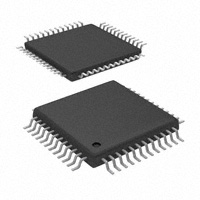


 工商网监
湘ICP备2023018690号
工商网监
湘ICP备2023018690号
