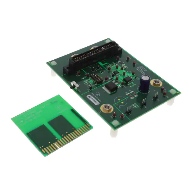
User’s Guide
Full-Featured –48-V Hot Swap Power
Manager (TPS2392 and TPS2393)
User’s Guide
�EVM IMPORTANT NOTICE
Texas Instruments (TI) provides the enclosed product(s) under the following conditions:
This evaluation kit being sold by TI is intended for use for ENGINEERING DEVELOPMENT OR EVALUATION
PURPOSES ONLY and is not considered by TI to be fit for commercial use. As such, the goods being provided
may not be complete in terms of required design-, marketing-, and/or manufacturing-related protective
considerations, including product safety measures typically found in the end product incorporating the goods.
As a prototype, this product does not fall within the scope of the European Union directive on electromagnetic
compatibility and therefore may not meet the technical requirements of the directive.
Should this evaluation kit not meet the specifications indicated in the EVM User’s Guide, the kit may be returned
within 30 days from the date of delivery for a full refund. THE FOREGOING WARRANTY IS THE EXCLUSIVE
WARRANTY MADE BY SELLER TO BUYER AND IS IN LIEU OF ALL OTHER WARRANTIES, EXPRESSED,
IMPLIED, OR STATUTORY, INCLUDING ANY WARRANTY OF MERCHANTABILITY OR FITNESS FOR ANY
PARTICULAR PURPOSE.
The user assumes all responsibility and liability for proper and safe handling of the goods. Further, the user
indemnifies TI from all claims arising from the handling or use of the goods. Please be aware that the products
received may not be regulatory compliant or agency certified (FCC, UL, CE, etc.). Due to the open construction
of the product, it is the user’s responsibility to take any and all appropriate precautions with regard to electrostatic
discharge.
EXCEPT TO THE EXTENT OF THE INDEMNITY SET FORTH ABOVE, NEITHER PARTY SHALL BE LIABLE
TO THE OTHER FOR ANY INDIRECT, SPECIAL, INCIDENTAL, OR CONSEQUENTIAL DAMAGES.
TI currently deals with a variety of customers for products, and therefore our arrangement with the user is not
exclusive.
TI assumes no liability for applications assistance, customer product design, software performance, or
infringement of patents or services described herein.
Please read the EVM User’s Guide and, specifically, the EVM Warnings and Restrictions notice in the EVM
User’s Guide prior to handling the product. This notice contains important safety information about temperatures
and voltages. For further safety concerns, please contact the TI application engineer.
Persons handling the product must have electronics training and observe good laboratory practice standards.
No license is granted under any patent right or other intellectual property right of TI covering or relating to any
machine, process, or combination in which such TI products or services might be or are used.
Mailing Address:
Texas Instruments
Post Office Box 655303
Dallas, Texas 75265
Copyright 2003, Texas Instruments Incorporated
2
�DYNAMIC WARNINGS AND RESTRICTIONS
It is important to operate this EVM within the maximum input voltage ranges specified in Table 2.
Exceeding the specified input range may cause unexpected operation and/or irreversible damage to the EVM.
If there are questions concerning the input range, please contact a TI field representative prior to connecting
the input power.
Applying loads outside of the specified output range may result in unintended operation and/or possible
permanent damage to the EVM. Please consult the EVM User’s Guide prior to connecting any load to the EVM
output. If there is uncertainty as to the load specification, please contact a TI field representative.
During normal operation, some circuit components may have case temperatures greater than 50°C. The EVM
is designed to operate properly with certain components above 50°C as long as the input and output ranges are
maintained. These components include but are not limited to linear regulators, switching transistors, pass
transistors, and current sense resistors. These types of devices can be identified using the EVM schematic
located in the EVM User’s Guide. When placing measurement probes near these devices during operation,
please be aware that these devices may be very warm to the touch.
Mailing Address:
Texas Instruments
Post Office Box 655303
Dallas, Texas 75265
Copyright 2003, Texas Instruments Incorporated
3
�SLUU155 – March 2003
Full-Featured –48-V Hot Swap Power Manager
(TPS2392 and TPS2393)
Andy Ripanti
Power Interface Products
ABSTRACT
The TPS2392 and TPS2393 integrated circuits are hot swap power managers optimized for use in
nominal –48-V systems. They operate over a supply voltage range of –20 V to –80 V, and are rated
to withstand spikes to –100 V. In conjunction with an external N-channel FET and sense resistor, they
can be used to enable live insertion of plug-in cards and modules in powered systems. Each device
provides load current slew rate control and peak magnitude limiting. Undervoltage and overvoltage
shutdown thresholds are easily programmed via a three-resistor divider network.
Contents
1
Introduction . . . . . . . . . . . . . . . . . . . . . . . . . . . . . . . . . . . . . . . . . . . . . . . . . . . . . . . . . . . . . . . . . . . . . . . . . 5
1.1 Features
...................................................................... 5
1.2 Description . . . . . . . . . . . . . . . . . . . . . . . . . . . . . . . . . . . . . . . . . . . . . . . . . . . . . . . . . . . . . . . . . . . . . . 5
2
The Full-Featured –48-V Hot Swap Controller EVM Kit . . . . . . . . . . . . . . . . . . . . . . . . . . . . . . . . . . 6
2.1 The Full-Featured –48-V Hot Swap Controller EVM Main Board . . . . . . . . . . . . . . . . . . . . . . . . 6
2.1.1
Module Description . . . . . . . . . . . . . . . . . . . . . . . . . . . . . . . . . . . . . . . . . . . . . . . . . . . . . . . 6
EVM Schematic Diagram and List of Materials . . . . . . . . . . . . . . . . . . . . . . . . . . . . . . . . . 7
2.1.2
2.2 The Full-Featured –48-V Hot Swap EVM Jumper Card . . . . . . . . . . . . . . . . . . . . . . . . . . . . . . . 10
2.2.1
Description . . . . . . . . . . . . . . . . . . . . . . . . . . . . . . . . . . . . . . . . . . . . . . . . . . . . . . . . . . . . 10
Jumper Card Schematic Diagram . . . . . . . . . . . . . . . . . . . . . . . . . . . . . . . . . . . . . . . . . . 11
2.2.2
2.3 Full-Featured –48-V Hot Swap EVM Operating Specifications . . . . . . . . . . . . . . . . . . . . . . . . . 12
3
Getting Started . . . . . . . . . . . . . . . . . . . . . . . . . . . . . . . . . . . . . . . . . . . . . . . . . . . . . . . . . . . . . . . . . . . . . 12
3.1 Equipment Requirements . . . . . . . . . . . . . . . . . . . . . . . . . . . . . . . . . . . . . . . . . . . . . . . . . . . . . . . . . 12
3.2 Verifying the EVM Operation . . . . . . . . . . . . . . . . . . . . . . . . . . . . . . . . . . . . . . . . . . . . . . . . . . . . . . 13
3.2.1
Equipment Setup . . . . . . . . . . . . . . . . . . . . . . . . . . . . . . . . . . . . . . . . . . . . . . . . . . . . . . . 13
3.2.2
Functional Test . . . . . . . . . . . . . . . . . . . . . . . . . . . . . . . . . . . . . . . . . . . . . . . . . . . . . . . . . 14
4
Using the EVM Kit to Evaluate the TPS2392 and TPS2393 . . . . . . . . . . . . . . . . . . . . . . . . . . . . . . 15
4.1 Supply Connections and Test Points . . . . . . . . . . . . . . . . . . . . . . . . . . . . . . . . . . . . . . . . . . . . . . . 15
4.2 Load Capacitors . . . . . . . . . . . . . . . . . . . . . . . . . . . . . . . . . . . . . . . . . . . . . . . . . . . . . . . . . . . . . . . . . 16
4.3 Changing the Current Limit Threshold . . . . . . . . . . . . . . . . . . . . . . . . . . . . . . . . . . . . . . . . . . . . . . 16
4.4 Changing the Inrush Slew Rate . . . . . . . . . . . . . . . . . . . . . . . . . . . . . . . . . . . . . . . . . . . . . . . . . . . . 17
4.5 Fault Timing With the TPS2392/93 . . . . . . . . . . . . . . . . . . . . . . . . . . . . . . . . . . . . . . . . . . . . . . . . . 18
4.6 Programming the UVLO and OVLO Thresholds and Hysteresis . . . . . . . . . . . . . . . . . . . . . . . . 18
4.7 TPS2392/93 Powergood Output (PG) . . . . . . . . . . . . . . . . . . . . . . . . . . . . . . . . . . . . . . . . . . . . . . 19
4
Full-Featured –48-V Hot Swap Power Manager
�SLUU155 – March 2003
1
Introduction
This User’s Guide describes the use and features of the full-featured –48-V hot swap evaluation module (EVM).
This EVM can be used to learn about the TPS2392 and TPS2393 hot swap power manager (HSPM) integrated
circuits from Texas Instruments. The TPS2392 and TPS2393 are negative voltage hot swap controllers intended
for use in systems needing to hot swap telecom distribution-level voltages. They integrate inrush current control,
peak current limiting, electronic circuit breaker, enable input, powergood reporting, overvoltage and
undervoltage protection, debounced insertion detection, and current fault indication. The EVM is a PCB-based
tool featuring either device, and can be used to evaluate device operation in simulated live insertion events.
1.1
Features
The following list highlights some of the features of the TPS2392 and TPS2393 device.
D
D
D
D
D
D
D
D
D
D
D
1.2
Wide input supply range of –20 V to –80 V
Transient rating to –100 V
Programmable current limit
Programmable current slew rate
Programmable UV/OV thresholds/hysteresis
Debounced insertion detection inputs
Open-drain power good (/PG) output
Fault timer to eliminate nuisance trips
Open-drain fault output (FAULT)
Enable input (EN)
14-pin TSSOP package
Description
The TPS2392 and TPS2393 integrated circuits are hot swap power managers optimized for use in nominal
–48-V systems. They operate over a supply voltage range of –20 V to –80 V, and are rated to withstand spikes
to –100 V. In conjunction with an external N-channel FET and sense resistor, they can be used to enable live
insertion of plug-in cards and modules in powered systems. Each device provides load current slew rate control
and peak magnitude limiting. Undervoltage and overvoltage shutdown thresholds are easily programmed via
a three-resistor divider network. In addition, two active-low, debounced inputs provide plug-in insertion
detection. A power good (PG) output enables downstream converters. The TPS2392 and TPS2393 also provide
the basic hot swap functions of electrical isolation of faulty cards, filtered protection against nuisance
overcurrent trips, and single-line fault reporting.
The TPS2392 latches off in response to current faults. The TPS2393 periodically retries the load, to test for the
continued existence of a fault.
Full-Featured –48-V Hot Swap Power Manager
5
�SLUU155 – March 2003
2
The Full-Featured –48-V Hot Swap Controller EVM Kit
The full-featured –48-V hot swap controller EVM kit is a two-board platform that enables designers to rapidly
learn about the TPS2392 and TPS2393 operation, and evaluate their performance during hot swap events. The
main evaluation board (TI board number SLUP189–001 or SLUP189–002) is divided into two sections, one
representing the backplane side of a typical telecom system, and the other containing the power interface
section of a hot swap capable plug-in card. On the main EVM PCB, the two subsections are isolated. The EVM
jumper card (TI board number SLUP190), when inserted into the main board’s P1 connector, provides a
mechanism for simulating hot swap events by abruptly applying power, ground and control signals on the
backplane side to their corresponding inputs on the plug-in side.
2.1
2.1.1
The Full-Featured –48-V Hot Swap Controller EVM Main Board
Module Description
The full-featured –48-V hot swap controller EVM main board is divided into two separate circuits. When oriented
such that the board nomenclature is upside right to the user, the left side of the board represents the backplane
side of the hot swap interface; the right side represents the plug-in module side. This half contains the power
isolation and control electronics comprising a hot swap interface that may be incorporated in a –48-V hot swap
plug-in board. In addition, the right side of the main board contains some additional switches and components
that can be used to facilitate device testing and for quick modifications of the plug-in characteristics. The two
PCB sections connect to a 44-pin PCB edge connector (P1). Mate and demate of the plug-in is accomplished
by inserting and removing the EVM jumper card.
The backplane side of the main board contains banana jacks for the connection of the –48-V power supply.
The plug-in side of the EVM board contains the TPS2392 or TPS2393 –48-V HSPM device, a power MOSFET
switch, and some configuration capacitors. Two through-hole patterns are provided on the load side for the
installation of large-value aluminum electrolytic capacitors. These capacitors simulate the input bulk
capacitance that may be found on the target module’s back-end supply plane. The EVM is supplied from the
factory with a 100-µF capacitor installed in one of these locations. The second pattern, connected in parallel
with the first, can be used to increase or otherwise modify the amount of load capacitance. With the TPS2392
and TPS2393, both inrush slew rate limiting and a fault time-out period are externally programmable using
capacitors. On the EVM main board, several options are provided for slew rate limiting, for quick comparison
of the effect of capacitor value on this function. The capacitors can be quickly switched in and out of the circuit
via the DIP switch. Fault timing programming is set up in a similar manner; some amount of capacitance is
hard-wired into the circuit, with the option of switching in additional capacitance.
The main board also contains some component patterns and connections to exercise the undervoltage (UVLO),
overvoltage (OVLO), and insertion detection functions, and a switch to toggle the device enable input. Two
possible circuits for interfacing the powergood output are also provided.
Test points are provided throughout the circuit for easy voltage monitoring via oscilloscope or voltmeter. The
test point connections are listed in Table 6.
The pictorial of the full-featured –48-V hot swap EVM top assembly is shown in Figure 1.
6
Full-Featured –48-V Hot Swap Power Manager
�SLUU155 – March 2003
Figure 1. Evaluation Module Main Board Top Assembly
2.1.2
EVM Schematic Diagram and List of Materials
The EVM main board schematic diagram is shown in Figure 2. The EVM main board list of materials is provided
in Table 1.
Full-Featured –48-V Hot Swap Power Manager
7
�+
+
SLUU155 – March 2003
Figure 2. –48-V Hot Swap Power Manager Evaluation Module Schematic
8
Full-Featured –48-V Hot Swap Power Manager
�SLUU155 – March 2003
Table 1. Evaluation Module List of Materials
REF DES
QUANTITY
DESCRIPTION
MANUFACTURER
PART NUMBER
–002
–001
U1
1
–
IC, full-featured –48 V hot swap controller, w/retry
Texas Instruments
TPS2393PW
U1
–
1
IC, full-featured –48 V hot swap controller, latching
Texas Instruments
TPS2392PW
U2
1
1
IC, linear, optocoupler, 30 V, h(FE) = 0.2 min.
Fairchild
4N25.S
TP8, TP15, TP18, TP19
4
4
Jack, test point, black
Farnell
240–333
TP1–TP7, TP9, TP10,
TP13, TP14, TP16, TP17,
TP20 – TP23
17
17
Jack, test point, red
Farnell
240–345
S1
1
1
Switch, slide, SPDT, right angle, 200 mA
E–Switch
EG1213
SW1
1
1
Switch, dip, 5 position, SPST
CTS
219–05MS
R7, R8
2
2
Resistor, 20 kΩ, 1 W, 5%
Vishay
CRCW2512–203J
R6
1
1
Resistor, 12 kΩ, 1 W, 5%
Vishay
CRCW2512–123J
R10
1
1
Resistor, 30 kΩ, 0.5 W, 5%
Vishay
CRCW2010–303J
R4
1
1
Resistor, 0.02 Ω, 0.5 W, 1%
Vishay–Dale
WSL–2010 .020 100 V, RDSon = 10.5
mΩ MAX
Vishay–Siliconix
SUB85N10–10
P1
1
1
Connector, 44 pin, PCB vertical, .100 cntrs
Tyco
530843–4
N/A
1
1
Plug, keying, connector, intercontact
Tyco
650025–2
J5 – J7
3
3
Header, 2 pin, single row, .10–C, .025sq., .230 head
Sullins
PTC36SAxN
J1 – J4
4
4
Jack, banana, non-insulated, PC mnt.
Pomona
3267
D2
1
1
Diode, zener, 5.6 V at 5 mA, 0.35 W
Vishay–Semi
BZX84C5V6
D3
1
1
Diode, dual, series, switching, 240 V, 0.35 W
Vishay–Semi
GSD2004S–E9
D1
1
1
Diode, LED, ultra bright red, GW type
Panasonic
LN1261CAL
C9
–
–
Capacitor, aluminum elec, 100 µF, 100 V, 20%
Panasonic
EEU–FC2A101
C8
1
1
Capacitor, aluminum elec, 100 µF, 100V, 20%
Panasonic
EEU–FC2A101
C7
1
1
Capacitor, ceramic, 1500 pF, 25 V, 20%, X7R
Vitramon
VJ0805Y152MXXA
C1
1
1
Capacitor, ceramic, 1000 pF, 25 V, 10%, X7R
Vitramon
VJ0805Y102KXXA
C5
–
–
Capacitor, ceramic, 0805
Standard
Standard
C4
1
1
Capacitor, ceramic, 0.1 µF, 16 V, 10%, X7R
Vitramon
VJ0805Y104KXJA
C6
1
1
Capacitor, ceramic, 0.082 µF, 16 V, 10%, X7R
Vitramon
VJ0805Y823KXJA
C3
1
1
Capacitor, ceramic, 0.047 µF, 16 V, 10%, X7R
Vitramon
VJ0805Y473KXJA
C2
1
1
Capacitor, ceramic, 0.01 µF, 16 V, 10%, X7R
Vitramon
VJ0805Y103KXJA
N/A
4
4
Spacer, nylon, hex, #6–32, 0.625”
Eagle
14HTSP020
N/A
4
4
Screw, nylon, round head, #6–32, 0.25”
Eagle
010632R025
N/A
1
1
PCB, FR–4, 2 layer, SMOBC, 4.71” x 3.60”, 0.062”
Texas Instruments
SLUP189
N/A
1
1
PCB, FR–4, 2 layer, SMOBC, jumper card
Texas Instruments
SLUP190
Full-Featured –48-V Hot Swap Power Manager
9
�SLUU155 – March 2003
2.2
2.2.1
The Full-Featured –48-V Hot Swap EVM Jumper Card
Description
The EVM jumper card is used to apply the –48-V supply voltage, present at the input banana jacks, to the supply
input of the main board’s plug-in side. Inserting and removing the jumper card into and out of the main board
P1 connector simulates hot swap events. There are no components mounted on the jumper card; it simply
makes the point-to-point connections to apply input power to the plug-in electronics. This mechanism allows the
EVM main board, which may have several scope probes and meter leads connected to it during use, to remain
stationary on the user’s bench.
A pictorial of the jumper card top layer is shown in Figure 3.
Figure 3. EVM Jumper Card Top Assembly
10
Full-Featured –48-V Hot Swap Power Manager
�SLUU155 – March 2003
2.2.2
Jumper Card Schematic Diagram
The EVM jumper card schematic diagram is shown in Figure 4.
Figure 4. EVM Jumper Card Schematic
There are no components installed on the jumper card, and consequently no list of materials required.
Full-Featured –48-V Hot Swap Power Manager
11
�SLUU155 – March 2003
2.3
Full-Featured –48-V Hot Swap EVM Operating Specifications
The full-featured –48-V hot swap EVM is intended to allow some degree of user reconfiguration. This allows
designers to set up the circuit to better represent the characteristics of their target application. Potential
modifications include changing the inrush limiting, the fault timing, and load characteristics. However, under no
circumstances should the EVM kit be operated beyond the absolute maximum conditions specified in Table 2.
Table 2. EVM Absolute Maximum Ratings(1),(2)
PARAMETER
Input voltage range, J1
MIN
MAX
UNITS
–0.3
100
V
Input voltage range, J5 (Jumper Card installed)
Input voltage range, J5(3)
100
V
30
V
Load current, J3
–5
A
Load return current, J4
5
A
85
°C
Ambient Operating Temperature Range
–40
NOTES: (1) Unless otherwise specified, voltages are with respect to the PCB –48V_IN
node at J2.
(2) Currents are positive into and negative out of the specified terminal.
(3) Relative to the VOUT– node at J4.
As supplied from the factory, the –48-V hot swap EVM is configured for operation under the following target
conditions, shown in Table 3.
Table 3. EVM Recommended Operating Conditions(1),(2)
PARAMETER
Input supply voltage, J1
Input supply voltage, J5(3)
MIN
NOM
MAX
UNITS
0
48
80
V
5
20
V
–1
Nominal load current, J3
–1
Nominal load return Current, J4
Operating temperature range
A
1
–40
A
85
°C
NOTES: (1) Unless otherwise specified, voltages are with respect to the PCB –48V_IN node at J2.
(2) Currents are positive into and negative out of the specified terminal.
(3) Relative to the VOUT– node at J4.
3
Getting Started
3.1
Equipment Requirements
The following test equipment is required to use the full-featured –48-V hot swap EVM .
•
•
•
12
Power supply, 80 VDC at 3 amps minimum
Oscilloscope
Digital voltmeter (DVM)
Full-Featured –48-V Hot Swap Power Manager
�SLUU155 – March 2003
3.2
Verifying the EVM Operation
The following procedure steps may be used to verify functional operation of the EVM after receipt.
3.2.1
Equipment Setup
On the EVM board, place the ENABLE switch S1 in the OFF position.
Set the DIP switches 1 through 4 of switch SW1 to the ON position.
Turn on power supply number 1 and adjust the output for about 48 V. Verify the supply current limit is set to allow
at least 3 amps. Turn on power supply number 2 and adjust its output to 5 V. Turn off the power supplies.
Connect the EVM and test equipment as shown in Figure 5.
PS No. 1
(+48 VDC)
PS No. 2
(+5 VDC)
+
+
–
J2 (–48V_IN)
J1 (–48V_RTN)
–
(VS) J5
(VOUT–) J4
TP8/TP15 (GND)
DIGITAL
VOLTMETER
CH 1
TP5
Full–Featured –48–V
VOLTS COM
CH 2
TP7
Evaluation Module
OSCILLOSCOPE
CH 3
Hot Swap Power Manager
TP6
TP1
TP14
(GND) TP8/TP15
CH 4
TP23
Connect leads as
desired
Figure 5. Full-Featured –48-V Hot Swap EVM Setup
On the oscilloscope, set the channel amplifiers to the following scales:
•
•
•
•
CH1: 5 V/div
CH2: 2 V/div
CH3: 5 V/div
CH4: 20 V/div
Set the scope to trigger on the rising edge of Channel 1, at about a 2.5-V level. Set the scope timebase to 10 ms,
and the trigger mode to NORMAL.
Full-Featured –48-V Hot Swap Power Manager
13
�SLUU155 – March 2003
3.2.2
Functional Test
Turn on both power supplies.
Insert the jumper card into the P1 connector, observing the proper insertion keying. On the EVM main board,
verify the red LED (D1) is OFF. Verify the voltage readings indicated in Table 4 are obtained at the corresponding
test points.
Table 4. Test Point Voltages (Outputs OFF)
TEST POINT
REFERENCE
VOLTAGE READING
TP1
TP8/TP15
Approx. 2.13 V
TP14
TP8/TP15
Approx. 0.94 V
TP20
TP22/J4
0 ± 200 mV
J6
TP22/J4
4.70 V min.
J7
TP22/J4
4.93 V min.
Place the ENABLE switch in the ON position. Verify the red LED (D1) remains off. The scope should have
acquired a sweep similar to that shown in Figure 6.
EN (5 V/div.)
IRAMP (2 V/div.)
FLTTIME (5 V/div.)
VOUT – (20 V/div.)
t – Time – 10 ms/div.
Figure 6. Load Ramp-Up Waveforms
The brief fault timing ramp which is shown in Figure 6 may or may not be present, depending on the actual values
of the timing parameters for the particular board being used. If the load voltage ramps to full input potential during
the initial reduced rate ramp period, then fault timing does not initiate.
The DMM can be used to verify that the voltages shown in Table 5 are present at the test points indicated.
Table 5. Test Point Voltages –– Outputs ON
TEST POINT
REFERENCE
VOLTAGE READING
TP20
TP22/J4
~ Input Supply Voltage
J6
TP22/J4
< 0.8 V
J7
TP22/J4
250 mV MAX
Either place the ENABLE switch in the OFF position, or remove the jumper card, to remove power from the
VOUT terminals.
14
Full-Featured –48-V Hot Swap Power Manager
�SLUU155 – March 2003
4
Using the EVM Kit to Evaluate the TPS2392 and TPS2393
Procedures similar to the steps of Section 3.2.2 for functional test of the EVM can also be used to continue
evaluation of the TPS2392 and TPS2393 hot swap controller devices. Additional details about the EVM features
are provided in this section.
4.1
Supply Connections and Test Points
Supply connections to the EVM should be made as shown in Figure 5. The backplane, 48-V supply (power
supply number 1 in Figure 5) connects to J1 and J2. The polarity of the circuit is such that the HI or (+) output
of the supply connects to J1, –48V_RTN. The LO or (–) jack connects to J2, –48V_IN. PCB header J5 (VS) is
used to connect an external pull-up source when using the EN1 and EN2 outputs of the module. This supply
is referenced to the VOUT– node.
The full-featured –48-V hot swap EVM contains numerous test points located throughout the circuit for
waveform monitoring. A list of the EVM test points and their associated signals is given in Table 6.
Table 6. Full-Featured –48-V Hot Swap EVM Test Points
TEST POINT
SIGNAL NAME
TP1
UVLO
Sense input for supply undervoltage detection.
TP2
INSA
Insertion detection input A.
TP3
INSB
Insertion detection input B.
TP4
FAULT
TP5
EN
TP6
FLTTIME
TP7
IRAMP
TP8
–VIN
DESCRIPTION
Load fault output of the TPS2392/93. On the EVM, this signal drives the
red LED.
Device enable input to turn on/off power to the load.
Fault timing waveform of the TPS2392/93.
Current ramp control output waveform.
Negative supply input and reference pin for the TPS2392/93. On the
EVM, this is connected to –48V_IN when the Jumper Card is inserted.
TP9
ISENS
Current sense input of the controller.
TP10
GATE
Gate drive for pass FET Q1.
TP13
DRNSNS
TP14
OVLO
Sense input for supply overvoltage detection.
TP15
–VIN
Secondary test point on device reference node (located near timing
capacitors).
TP16
TP17
VOUT
VOUT+
TP18
TP19
VIN
–VIN
Sense input of the controller for load voltage status.
Additional su
supply
ly high side test points
oints (located on in
input
ut side of board,
near TPS2392/93 power pin).
Secondary negative supply
su ly input
in ut test points.
oints. On the EVM, these are
connected to –48V_IN when the Jumper Card is inserted.
TP20
TP21
VOUT
VOUT+
High side of switched
s itched (load) output
o tp t power.
po er
VOUT
VOUT–
Lo side of sswitched
Low
itched (load) o
output
tp t po
power.
er
TP22
TP23
Full-Featured –48-V Hot Swap Power Manager
15
�SLUU155 – March 2003
4.2
Load Capacitors
Capacitor patterns C8 and C9 are available on the EVM for installation of components to represent the module
input bulk capacitance; i.e., the load capacitance seen by the hot swap interface circuit. As supplied from the
factory, the EVM contains a 100-µF aluminum electrolytic installed at C8. Further customization to approximate
the user’s application can be done using either C8 or C9. When installing capacitors in these mounting locations,
care should be taken to observe the polarity marking on the PCB silkscreen, and to use appropriately rated
capacitors for voltage withstanding. Generally, telecom applications should use 100-V minimum rated
capacitors.
Banana jacks J3 and J4 are also connected across the output terminals, in parallel with C8 and C9. These jacks
can be used to connect additional loads to the EVM board.
4.3
Changing the Current Limit Threshold
During power-up of a plug-in card, the TPS2392 and TPS2393 limit the peak inrush current drawn by the
discharged bulk capacitance. The LCA senses load current as the drop across an external sense resistor.
Current is regulated by slewing the gate of the pass FET to maintain the voltage drop at an internally set level,
nominally 40 mV. Therefore, the peak current level can be established by selecting the appropriate sense
resistor value. On the –48-V Hot Swap EVM, this resistor is R4. The default value of R4 is 20 mΩ. To modify
the current limit threshold, a new sense resistor value can be determined from Equation 1.
R4 v VMAX
IMAX
(1)
where:
•
•
VMAX is the sense voltage limit, and
IMAX is the desired current limit threshold.
Using the device minimum value of 33 mV for VMAX along with the required minimum load current ensures that
minimum amount of current can always be supplied to the load. For example, a particular line card is expected
to draw a maximum of 1.2 A, when the power bus is at its operating minimum level of –33 V, once the card is
powered up and operating normally. For this load characteristic, a sense resistor value less than 33 mV/1.2 A,
or 27 mΩ, would be selected. A 25-mΩ resistor is generally the closest standard value readily available; smaller
values also work, but with a corresponding increase in the maximum current limit.
16
Full-Featured –48-V Hot Swap Power Manager
�SLUU155 – March 2003
4.4
Changing the Inrush Slew Rate
The TPS2392 and TPS2393 also feature slew rate limiting as current is ramped to charge the load capacitance.
The slew rate is easily programmed, once the sense resistor is determined, with a small-value capacitor
connected between the IRAMP and –VIN pins. The EVM comes equipped with three preset capacitor values,
selectable either individually or combined by closing the appropriate DIP switches of SW1. The default values
of the capacitors, and the corresponding nominal slew rates, are given in Table 7.
Table 7. –48-V Hot Swap EVM Default Slew Rates
SW1 DIP
REF DES
INSTALLED VALUE
SLEW RATE (A/S)
1
C1
1000 pF
5000
2
C2
0.01 µF
500
3
C3
0.047 µF
106
The EVM can be used to get an illustration of the relationship between current limit, inrush slew rate, load values,
and the circuit’s fault timing requirements. With DIP switch SW1–1 only closed, the fastest of the preset slew
rates is selected, and only the hard-wired timing capacitor C6 is connected to the TPS2392 or TPS2393
controller. However, this is sufficient to allow the bulk capacitor C8 to fully charge, from 0 volts, across the full
range of input supply voltages, down to –80 V. This can be observed by connecting input power as shown in
Figure 5, displaying the VOUT– node on an oscilloscope, and enabling the device.
To observe the controller response to a load that does not charge up as expected (a shorted or otherwise
excessive load), set switches SW1–1, SW1–2, and SW1–3 to the ON position. This greatly reduces the inrush
(load charging) current slew rate at turn-on, with a corresponding increase in the amount of time needed to
successfully charge the intended load. Increase the supply level to about 60 V to 80 V, and again enable the
device. In this case, the voltage ramp time is excessively long relative to the programmed fault timer; the
controller times out and turns off the load (See Note below). This can be seen from the illumination of the red
LED. (For the TPS2393, the LED may flash briefly then turn off, indicating capacitor charging ultimately
completed on a successive retry.) If this combination represented the parameters of the target plug-in module,
then the timing capacitance of C6 and C4 (SW1–4 closed) would be more appropriate. The intended load, in
this case, the 100-µF capacitor, can again be charged up over the input voltage range.
NOTE: Due to tolerances of various EVM parameters, some units may not fault out under these
conditions. Generally, this is due to the fact that the amount of voltage ramping during the
reduced–rate turn–on period varies from device to device. Some units may be able to charge the
load almost completely during this period, when fault timing is inhibited. A more severe load fault
is needed to view the fault response. Additional capacitance, or even a resistor, can be connected
across the VOUT terminals, J3(+) and J4(–) or at C9. If the user is confident the module is operating
correctly, the load can also be shorted out to do this.
The inrush slew rate can be changed, to better match the application requirement, by replacing any capacitor
C1, C2 or C3. The PCB patterns are sized for 0805 ceramic chip capacitors. Use equation 2 to calculate the
new ramp capacitor, CRAMP, value in microfarads.
C RAMP +
11
100
R4
ǒdtdiǓ
(2)
MAX
where:
•
•
R4 is the selected sense resistor value, in ohms, and
(di/dt)MAX is the desired maximum slew rate, in amps/second.
Full-Featured –48-V Hot Swap Power Manager
17
�SLUU155 – March 2003
4.5
Fault Timing With the TPS2392/93
Whenever the hot swap controller is limiting current to the load, an on-chip timer is monitoring this operation
against an established time limit. The timeout period is generated by the constant-current charging of a capacitor
at the FLTTIME pin. If current regulation ceases prior to expiration of the timer, the capacitor is discharged, and
normal steady-state operation of the load either starts or resumes. However, if the timer expires, then the pass
FET is turned off, disabling power to the load, and the FAULT output is asserted.
On the EVM, several capacitor patterns are provided for adding or otherwise modifying the timeout period.
Capacitor C6 is hard-wired to the device FLTTIME pin, and provides a minimum fault timer for the default load.
C4 and C5 can be switched into the circuit via DIP switches SW1–4 and SW1–5, respectively. The EVM ships
from the factory with a 0.1-µF capacitor installed at C4; C5 is not populated for easier subsequent user
modification as required.
If the target application requires fault timing other than provided by the default EVM setup, a new value of timing
capacitor can be calculated from Equation 3. When selecting from the readily available capacitor values for the
Equation 3 result, default to a slightly larger, rather than smaller, capacitor.
C FLT +
55
t FLT
3.75
(3)
where:
•
•
4.6
CFLT is the calculated value in microfarads, and
tFLT is the desired timeout period in seconds
Programming the UVLO and OVLO Thresholds and Hysteresis
The UVLO and OVLO pins can be used to set the circuit undervoltage and overvoltage thresholds (VUV and VOV,
respectively). When the input supply is below VUV or above VOV, the GATE pin is held low, disconnecting power
from the load, and the PG output is deasserted. When input voltage is within the UV/OV window, the GATE drive
is enabled, assuming all other input conditions are valid for turn-on.
Threshold hysteresis is also externally programmable. Internal current sources are switched to the UVLO and
OVLO pins whenever the corresponding input voltage exceeds the nominal 1.4-V reference. Please refer to the
TPS2392/93 data sheet (TI Literature Number SLUS536) for additional details about the UVLO and OVLO
comparator operation.
On the –48-V hot swap EVM, the VUV and VOV thresholds are individually programmed via the three-resistor
divider R1, R2, and R3 (refer to Figure 2). The factory-installed resistor values result in the following nominal
voltage thresholds.
18
Full-Featured –48-V Hot Swap Power Manager
�SLUU155 – March 2003
Table 8. Nominal UVLO and OVLO settings.
PARAMETER
DESCRIPTION
VALUE (V)
VUV_L
VUV_H
VOV_L
UVLO threshold, supply low (VIN < VUV)
UVLO threshold, supply high (VIN > VUV)
32.8
OVLO threshold, supply low (VIN < VOV)
72.6
VOV_H
OVLO threshold, supply high (VIN > VOV)
70.5
30.8
The thresholds are easily modified by changing the resistor values. When the desired trip voltages and the UV
hysteresis have been established for the protected load, new values are determined as follows. Generally, the
process is simplest by first selecting the top leg of the divider (R1) needed to obtain the desired hysteresis. This
value is calculated from Equation 4.
R1 +
V HYS_UV
10 mA
(4)
where VHYS_UV is the amount of undervoltage hysteresis.
Once a value for R1 is selected, it is used to calculate R2 and R3 using Equations 5 and 6.
R2 +
R3 +
ȱ
V UV_L
1*
ȧ
ǒVUV_L * 1.4Ǔ Ȳ ǒVOV_L ) 10*5
1.4
R1
ȱ
V UV_L
ȧ
ǒVUV_L * 1.4Ǔ ȲǒVOV_L ) 10*5
1.4
R1
ȳ
ȧ
R1Ǔȴ
(5)
ȳ
ȧ
R1Ǔȴ
(6)
where:
•
•
4.7
VUV_L is the UVLO threshold when the input supply is low; i.e., less than VUV, and
VOV_L is the OVLO threshold when the input supply is low; i.e., less than VOV
TPS2392/93 Powergood Output (PG)
The –48-V hot swap EVM contains two possible circuits for interfacing to the device PG output pin. The outputs
of these circuits are available at the PCB headers J6 and J7 as the EN1 and EN2 signals, respectively. An
example application of these signals is to drive the enable input of downstream converters. As such, both
outputs are referenced to the VOUT– node of the EVM, as this would be the low side of input power to the brick.
The EN1 output is generated via the resistive translation of the device PG output. The EVM schematic of
Figure 2 shows the circuit details. This active-low output is capable of sinking a minimum of 10 µA at a maximum
output voltage of 0.8 V(TTL–compatible VOL), across the complete range of the 48-V input supply and ambient
operating temperature. (The default UVLO and OVLO thresholds are assumed.)
The EN2 output demonstrates an isolated signal implementation using an opto device. The EVM schematic
shows the circuit details. This active-low output is capable of sinking a minimum of 150 µA across the complete
range of input supply voltage and ambient operating temperature.
The use of these enable signals requires a pull-up source at the VS input, J5. See Tables 2 and 3 for the
requirements of the VS supply.
Full-Featured –48-V Hot Swap Power Manager
19
�IMPORTANT NOTICE
Texas Instruments Incorporated and its subsidiaries (TI) reserve the right to make corrections, modifications,
enhancements, improvements, and other changes to its products and services at any time and to discontinue
any product or service without notice. Customers should obtain the latest relevant information before placing
orders and should verify that such information is current and complete. All products are sold subject to TI’s terms
and conditions of sale supplied at the time of order acknowledgment.
TI warrants performance of its hardware products to the specifications applicable at the time of sale in
accordance with TI’s standard warranty. Testing and other quality control techniques are used to the extent TI
deems necessary to support this warranty. Except where mandated by government requirements, testing of all
parameters of each product is not necessarily performed.
TI assumes no liability for applications assistance or customer product design. Customers are responsible for
their products and applications using TI components. To minimize the risks associated with customer products
and applications, customers should provide adequate design and operating safeguards.
TI does not warrant or represent that any license, either express or implied, is granted under any TI patent right,
copyright, mask work right, or other TI intellectual property right relating to any combination, machine, or process
in which TI products or services are used. Information published by TI regarding third–party products or services
does not constitute a license from TI to use such products or services or a warranty or endorsement thereof.
Use of such information may require a license from a third party under the patents or other intellectual property
of the third party, or a license from TI under the patents or other intellectual property of TI.
Reproduction of information in TI data books or data sheets is permissible only if reproduction is without
alteration and is accompanied by all associated warranties, conditions, limitations, and notices. Reproduction
of this information with alteration is an unfair and deceptive business practice. TI is not responsible or liable for
such altered documentation.
Resale of TI products or services with statements different from or beyond the parameters stated by TI for that
product or service voids all express and any implied warranties for the associated TI product or service and
is an unfair and deceptive business practice. TI is not responsible or liable for any such statements.
Mailing Address:
Texas Instruments
Post Office Box 655303
Dallas, Texas 75265
Copyright 2003, Texas Instruments Incorporated
�