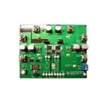
TPS2412/13 Evaluation Module,
HPA227
User's Guide
January 2007
Power Supply MAN
sluu267
�TPS2412/13 Evaluation Module, HPA227
User's Guide
Literature Number: sluu267
January 2007
�User's Guide
sluu267 – January 2007
TPS2412/13 Evaluation Module, HPA227
1
Purpose
This user guide is to facilitate operation of the TPS2412/13 Evaluation Module, HPA227. It is used by an
engineer or technician and supplements the TPS2412/13 datasheet, HPA227 schematics, and HPA227
circuit board labeling.
2
Introduction
The TPS2412 controls an N-channel MOSFET to operate in circuit as an ideal diode. The MOSFET
source and drain voltages are monitored by TPS2412 pins A and C. The TPS2412 drives the MOSFET
gate high if VAC exceeds 10 mV, and turns the MOSFET off if VAC falls below a threshold that is both
programmable and dependent on the choice of TPS2412 or TPS2413.
The TPS2412 has a fixed turn off point of 3.0 mV VAC.
TPS2413 is similar to TPS2412 but has a resistor programmable MOSFET turn off point. The TPS2413
can even be set to slightly negative allowing some back current.
Figure 1 shows the conventional wire-OR of power supplies with diodes. Each diode D1 and D2 is
replaced by a TPS2412 and MOSFET eliminating the voltage and power loss in the diode.
The evaluation module is set up to wire-OR two power supplies for redundant power to a load using two
TPS2410s and MOSFETs. This document contains setup and user information about this evaluation
module to assist with the operation of TPS2412.
+V1
TPS2412
PS1
D1
GND
+V
LOAD
GND
+V2
D2
PS2
GND
TPS2412
Figure 1. Conventional Wire-OR Power Supplies
sluu267 – January 2007
TPS2412/13 Evaluation Module, HPA227
3
�www.ti.com
Materials Needed
Reference Figure 2, a block diagram of the HPA227.
• The 5-V supply is jumper selected to power VDD on the TPS2412s and the glitch circuit if the control
voltage is less than 3.0 V.
• The Glitch maker, discussed in the Test Methods section applies a 1-Ω load to the input supply for 1
ms. This disruption allows the user to scope test points and observe system recovery.
• The RSET resistor is used to program the turn off point of the TPS2411.
Glitch
Maker
PS1
Channel 1
TPS2412
Output
FET
+5V PS
Load
PS2
Channel 2
TPS2412
Output
FET
Figure 2. EVM Block Diagram
3
Materials Needed
TI
•
•
•
Supplied:
TPS2412 evaluation module
TPS2412 reference design documentation
TPS2412 datasheet
User Supplied:
• Two power supplies for wire–OR to load, up to 15 A
• 1-V to 5-V power supply for VDD
• Power supply cables
• Load-active load, power resistors or actual load
• Oscilloscope
• Current probe
• Differential probe
4
TPS2412/13 Evaluation Module, HPA227
sluu267 – January 2007
�www.ti.com
Jumper Description
4
Jumper Description
4.1
Jumpers J1, J2, J8, J9
VDD can be powered by the input power supply pin A, Jump J1-2, 3 and J9-2, 3. When it is powered by
the load, pin C, jump J1-1, 2 and J9-1, 2. If A and C are less than 3 V, connect the 5 V to VDD, jumper
J1-1 to J2 -2 and J8-1 to J9-2.
4.2
J13
Jumper J8 is the gate voltage for the Glitch FET. Jump J13-2, 3 when the PS1 voltage is greater than 5
volts. Jump J13-1, 2 to use the 5 volt supply when PS1 is less than 5 volts.
4.3
J14
J14 is used to short out the current limit resistor on glitching the power supply. This jumper is installed
only when the voltage is less than 3 volts and a glitch is not generated because of current limit.
5
Procedure
5.1
Jumper Set-Up
An initial jumper setup is recommended in Table 1. The module has flexibility to operate in other modes.
Change jumpers to operate in other configurations as required after getting started. After the initial setup,
reference the schematic and set jumpers as required for testing. Other J reference designators on the
schematic are simple connectors.
Table 1. Initial Jumper Settings
Jumper
Function
Selection
J1
5 V to VDD, CH1
Open
J2
A or C to VDD, CH1
Jumper A – VDD
Comment
Connects A
J8
5 V to VDD, CH2
Open
J9
A or C to VDD, CH2
Jumper A - VDD
Connects A
J13
PS1 to Glitcher
Jumper PS1 to Glitcher
Connects PS1
J14
Glitcher
Open
Shorts 1 Ω
sluu267 – January 2007
TPS2412/13 Evaluation Module, HPA227
5
�www.ti.com
Procedure
5.2
Power Supply Connection
Connect the power supplies and load to the TPS2410 test card as shown in Table 2. Loading less than 30
A is safe for IRl3713S. The load can be a test load or the actual system load.
Table 2. Power Supply Connection
Connection
Supply
PS1
PS2
5.3
Terminal
+V
PS1, J3
GND
PS1GND, J27
+V
PS2, J10
GND
PS2GND, J11
5V
5V
J15-2
5GND
GND
J15-1
Load +
Load
J5
Load -
GND
J7
Test Points
Table 3 lists some common test points for observation. There are more test points shown on the
Schematic.
Table 3. Common Test Points
5.4
Function
TP Channel 1
TP Channel 2
TP11
A
TP3
C
TP1
TP9
GATE
TP6
TP14
RSET
RSET is used in TPS2411 to program the MOSFET turn-off point. The RSET calculation from the datasheet
is:
æ
ö
-500
RSET = ç
÷
è VOFF - 0.003 ø
Calculate the RSET resistor and install. The component reference designators for both channels are
summarized in Table 4.
Table 4. Table 5, RSET Resistor Setting
5.5
RSET
CH1
CH2
Resistor
R2
R4
Test Methods
The EVM has a few operating modes to view the system response. The user can make modifications to
the EVM to test in other ways.
6
TPS2412/13 Evaluation Module, HPA227
sluu267 – January 2007
�www.ti.com
Procedure
5.6
Adjust Input Power Supplies
Vary the input voltages to observe system behavior. Jumpers can be set as in Table 1. Turn the power
supplies to the application typical 12 V. The load is shared between the supplies. Both gates will be on
and the power supply current meters show output. Decrease one supply voltage slightly and note the gate
on that channel pass FET turn off and the other channel FET gate increases to keep the FET on to supply
the load. Observe the FET gates with a scope. With a voltmeter, verify VDS for the on channel to be tens
of millivolts.
5.7
Glitch Maker
Set power supplies up for equal or slight differential voltage so that the PS1 supply is contributing to the
load. Press momentary switch S1, labeled PULSE. The switch closure places a 1-Ω load across the input
power supply for 1 ms. Observe the effect of an input power supply glitch at the MOSFET gates and load
voltage.
5.8
Input Power Supplies
Input change can be tested by cycling power, opening input, hot plugging, and shorting the supply.
5.9
Load change
A dynamic change to the load can be made by switching additional load on or off with an external switch.
Some power load test equipment can be used to dynamically change the load.
sluu267 – January 2007
TPS2412/13 Evaluation Module, HPA227
7
�www.ti.com
Schematic/Board Layout Diagrams
6
Schematic/Board Layout Diagrams
+
+
+
+
+
+
Figure 3. TPS2412/13 Schematic
8
TPS2412/13 Evaluation Module, HPA227
sluu267 – January 2007
�www.ti.com
Schematic/Board Layout Diagrams
Figure 4. TPS2412/13 Layout
sluu267 – January 2007
TPS2412/13 Evaluation Module, HPA227
9
�www.ti.com
List of Materials
7
List of Materials
Table 5. List of Materials for the TPS2412/13 (1) (2) (3) (4)
REF DES
COUNT
DESCRIPTION
C1, C2, C7, C8, C9,
C10
6
Capacitor, OSCON, SM, 100 µF, 20 V, 20%, G-case
Sanyo
20SVP100M
C15
1
Capacitor, ceramic, 0.1 µF, 16 V, X5R, 20%, '0603
STD
STD
C17
1
Capacitor, ceramic, 1 µF, 25 V, X5R, 20%, '0805
Panasonic
ECJ2FB1E105M
C18, C19, C20,
C21, C22, C23, C24
7
Capacitor, ceramic, 22 µF, 25 V, X5R, 20%, '1210
Panasonic
ECJ4YB1E226M
C3, C11
2
Capacitor, ceramic, 0.01 µF, 25 V, X7R, 20%, '0603
STD
STD
C4, C12
2
Capacitor, ceramic, 2200 pF, 50 V, X7R, 10%, 0603
STD
STD
J1, J8, J14
3
Header, 2 pin, 100-mil spacing, (36-pin strip), 0.100
inch x 2
Sullins
PTC36SAAN
J15
1
Terminal block, 2-pin, 6-A, 3.5mm, 0.27 x 0.25 inch
OST
ED1514
J2, J9, J13
3
Header, 3 pin, 100-mil spacing, (36-pin strip), 0.100
inch x 3
Sullins
PTC36SAAN
J3, J4, J5, J7, J10,
J11
6
Screw terminal, 0.310 x 0.310 inch
Keystone
7693
Q1, Q2, Q3
3
MOSFET, N-channel, 30 V, 30 A, RDS 3 mΩ,
PWRPAK S0-8
Vishay
Si7336ADP
R1, R3
2
Resistor, chip, 10 Ω,1/16 W, 1%, 0603
STD
STD
R2, R4
0
Resistor, chip, DNP, 1/16 W, 1%, 0603
STD
STD
R5
1
Resistor, power metal strip, 1 Ω, 2 W, 1%, 4527
Panasonic
WSR2 1R000 J EA
R6
1
Resistor, chip, 10 Ω, 1/16 W, 1%, 0603
STD
STD
R7
1
Resistor, chip, 1 kΩ, 1/16 W, 1%, 0603
STD
STD
R8
1
Resistor, chip, 2 kΩ, 1/16 W, 1%, 0603
STD
STD
S1
1
Switch, 1P1T, 20 mA, 15 V, 0.240 x 0.256
Panasonic
EVQPAC04M
SH1, SH2
2
Short jumper, 0.125 x 0.125 inch
TP1, TP2, TP3,
TP4, TP5, TP6,
TP7, TP9, TP10,
TP11, TP12, TP13,
TP14, TP15
14
Test point, white, thru hole, 0.185 x 0.135 inch
Keystone
5012
TP8, TP16, TP17,
TP18, TP19
5
Test point, SM, 0.150 x 0.090,
Keystone
5016
U1, U2
2
N+1 and O-Ring Power Rail Controller, TSSOP-8
TI
TPS241xPW
(1)
(2)
(3)
(4)
10
MFR
PART NUMBER
These assemblies are ESD sensitive, ESD precautions shall be observed.
These assemblies must be clean and free from flux and all contaminants. Use of no clean flux is not acceptable.
These assemblies must comply with workmanship standards IPC-A-610 Class 2.
Ref designators marked with an asterisk ('**') cannot be substituted. All other components can be substituted with equivalent
MFG's components.
TPS2412/13 Evaluation Module, HPA227
sluu267 – January 2007
�EVM WARNINGS AND RESTRICTIONS
It is important to operate this EVM within the input/output voltage range of 0.8 V to 18 V +/-5%.
Exceeding the specified input range may cause unexpected operation and/or irreversible
damage to the EVM. If there are questions concerning the input range, please contact a TI
field representative prior to connecting the input power.
Applying loads outside of the specified output range may result in unintended operation and/or
possible permanent damage to the EVM. Please consult the EVM User’s Guide prior to
connecting any load to the EVM output. If there is uncertainty as to the load specification,
please contact a TI field representative.
During normal operation, some circuit components may have case temperatures greater than
50°C. The EVM is designed to operate properly with certain components above 50°C as long
as the input and output ranges are maintained. These components include but are not limited
to linear regulators, switching transistors, pass transistors, and current sense resistors. These
types of devices can be identified using the EVM schematic located in the EVM User’s Guide.
When placing measurement probes near these devices during operation, please be aware
that these devices may be very warm to the touch.
Mailing Address:
Texas Instruments
Post Office Box 655303
Dallas, Texas 75265
Copyright © 2001, Texas Instruments Incorporated
�IMPORTANT NOTICE
Texas Instruments Incorporated and its subsidiaries (TI) reserve the right to make corrections, modifications,
enhancements, improvements, and other changes to its products and services at any time and to
discontinue any product or service without notice. Customers should obtain the latest relevant information
before placing orders and should verify that such information is current and complete. All products are sold
subject to TI’s terms and conditions of sale supplied at the time of order acknowledgment.
TI warrants performance of its hardware products to the specifications applicable at the time of sale in
accordance with TI’s standard warranty. Testing and other quality control techniques are used to the extent
TI deems necessary to support this warranty. Except where mandated by government requirements, testing
of all parameters of each product is not necessarily performed.
TI assumes no liability for applications assistance or customer product design. Customers are responsible
for their products and applications using TI components. To minimize the risks associated with customer
products and applications, customers should provide adequate design and operating safeguards.
TI does not warrant or represent that any license, either express or implied, is granted under any TI patent
right, copyright, mask work right, or other TI intellectual property right relating to any combination, machine,
or process in which TI products or services are used. Information published by TI regarding third-party
products or services does not constitute a license from TI to use such products or services or a warranty or
endorsement thereof. Use of such information may require a license from a third party under the patents or
other intellectual property of the third party, or a license from TI under the patents or other intellectual
property of TI.
Reproduction of information in TI data books or data sheets is permissible only if reproduction is without
alteration and is accompanied by all associated warranties, conditions, limitations, and notices.
Reproduction of this information with alteration is an unfair and deceptive business practice. TI is not
responsible or liable for such altered documentation.
Resale of TI products or services with statements different from or beyond the parameters stated by TI for
that product or service voids all express and any implied warranties for the associated TI product or service
and is an unfair and deceptive business practice. TI is not responsible or liable for any such statements.
Following are URLs where you can obtain information on other Texas Instruments products and application
solutions:
Products
Applications
Amplifiers
amplifier.ti.com
Audio
www.ti.com/audio
Data Converters
dataconverter.ti.com
Automotive
www.ti.com/automotive
DSP
dsp.ti.com
Broadband
www.ti.com/broadband
Interface
interface.ti.com
Digital Control
www.ti.com/digitalcontrol
Logic
logic.ti.com
Military
www.ti.com/military
Power Mgmt
power.ti.com
Optical Networking
www.ti.com/opticalnetwork
Microcontrollers
microcontroller.ti.com
Security
www.ti.com/security
Low Power Wireless
www.ti.com/lpw
Telephony
www.ti.com/telephony
Mailing Address:
Video & Imaging
www.ti.com/video
Wireless
www.ti.com/wireless
Texas Instruments
Post Office Box 655303 Dallas, Texas 75265
Copyright © 2007, Texas Instruments Incorporated
�