Using the TPS2420, TPS2421-1 and TPS2421-2
User's Guide
Literature Number: SLUU343
January 2009
�User's Guide
SLUU343 – January 2009
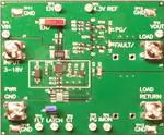
TPS2420 Hot Swap Controller System Test Board
This user’s guide describes the setup and operation of the TPS2420 system test board.
1
Introduction
This user’s guide describes the features of the TPS242X EVM. The TPS242X schematic, layout and List
of Materials are provided as well as a setup and getting started.
2
Description
The EVM is a 3 V to 18 V module using the TPS2420/21 hot swap controller with integrated MOSFET. At
power on, the output is power limited to control inrush current and protect the MOSFET. On an
over-current condition, the controller interrupts power to the load at high speed and signals load status.
Operating current, fault current and fault timer settings are hardware programmable.
2.1
Applications
2.1.1
Server
• Plug-In Circuit Boards
• RAID / Disk Drive
2.1.2
Telecom
• ATCA
• Micro-ATCA
2
TPS2420 Hot Swap Controller System Test Board
SLUU343 – January 2009
Submit Documentation Feedback
�Block Diagram
www.ti.com
2.2
Features
•
•
•
•
•
•
•
•
•
•
•
3
3-V to 18-V Operation
Controlled Inrush Current
Fast Circuit Breaker Control
Hardware Programmable
– Operating Current
– Fault Current
– Fault Timer to Avoid Nuisance Tripping
– Latch Off or Retry (TPS2420 is pin selectable, TPS2421-1 is latch-off only and TPS2421-2 is re-try
only.)
LED status display
A Slide Switch Controls the ENABLE Signal.
The Area Under the TPS2420/1 is Copper Pour with Vias to the Internal Ground to take Advantage of
the Power Pad Package.
A Transorb is On-Board for Over-Voltage Input Protection
A Common Diode at the Output Prevents a Negative Spike if the Load is Removed While Powered On
Programmable IMON Voltage Readout of the Output Current is Preset to 0.31 V / A
Test Points Available to Monitor Circuit Operation
Block Diagram
POWER
TPS2420/1
LOAD+
INDICATORS
ENABLE
GND
LOAD-
Figure 1. EVM Block Diagram
SLUU343 – January 2009
Submit Documentation Feedback
TPS2420 Hot Swap Controller System Test Board
3
�Schematic
4
www.ti.com
Schematic
Figure 2. TPS2420 Schematic
4
TPS2420 Hot Swap Controller System Test Board
SLUU343 – January 2009
Submit Documentation Feedback
�List of Materials
www.ti.com
5
List of Materials
This is the List of Material for the TPS242X EVM
Table 1. List of Materials
COUNT
REF DES
DESCRIPTION
PART NUMBER
MFR
2
C1, C3
Capacitor, ceramic, 0.1 µF, 603
STD
muRata
2
C2, C6
Capacitor, ceramic, 0.1 µF, 603
STD
muRata
1
C4
Capacitor, ceramic, 10V , 0.56 µF, 805
STD
muRata
1
C5
Capacitor, ceramic, 25 V, 1 µF, 1206
STD
muRata
1
D1
Diode, LED, red, 20 mA, 0.9 mcd, 0.068 x 0.049 inch
LN1271R
Panasonic
1
D2
Diode, LED, green, 20 mA, 0.9 mcd, 0.068 x 0.049 inch
LN1371G-(TR)
Panasonic
1
D3
Diode, Zener, 4.3 V, SOT23
MMBZ5229B
Motorola
1
D4
Diode, SMT TVS 400 W, 1 A, 15 V, SMA
SMAJ15A
Diodes
1
D5
Diode, Schottky, 1000 mA, 30 V, SOD123
MBR130LSFT1
STD
4
J1, J2, J4, J5
Screw terminal, 0.310 x 0.310 inch
7693
Keystone
1
J3
Header, 2 pin, 100-mil spacing, (36-pin strip), 0.100
inch x 2
PTC36SAAN
Sullins
2
Q1, Q2
Bipolar, PNP, xx-V, yy-mA, zz-W, SOT23
MMBT3906LT1
On Semi
1
R1
Resistor, chip, 0.5 W, 1%, 499 Ω, 2512
STD
STD
1
R11
Resistor, chip, 1/16 W, 1%, 24.9 kΩk, 603
STD
Vishay
1
R12
Resistor, chip, 1/16 W, 1%, 40.2 kΩ, 603
STD
Vishay
1
R13
Resistor, chip, 1/16 W, 1%, 49.9 kΩ, 603
STD
Vishay
2
R2, R3
Resistor, chip, 1/16 W, 5%, 10 kΩ, 603
STD
Vishay
2
R4, R5
Resistor, chip, 1/16 W, 1%, 1 kΩ, 603
STD
Vishay
1
R6
Resistor, chip, 1/16 W, 1%, 10 kΩ, 603
STD
Vishay
2
R7, R9
Resistor, chip, 1/16 W, 5%, 20 kΩ, 603
STD
Vishay
2
R8, R10
Resistor, chip, 1/10 W, 5%, 300 Ω, 805
STD
Vishay
1
S1
Switch, SPDT, slide, PC mount, 500 mA, 0.400 x 0.100
inch
09-03201-02
EAO
9
TP1, TP2, TP3, Test point, white, thru hole, 0.125 x 0.125 inch
TP4, TP5, TP6,
TP7, TP8, TP9
5012
Keystone
4
TP10, TP11,
TP12, TP13
Test point, SM, 0.150 x 0.090, 0.185 x 0.135 inch
5016
Keystone
0
TP14, TP15,
TP16, TP17
Test point, 0.062 Hole, 0.250 inch
5012
Keystone
1
U1
0 to 12V Integrated FET Hot Swap, QFN-16
TPS2420RSA
TI
1
U2
0 to 12V Integrated FET Hot Swap, SO8[DDA]
TPS2421-1DDA
TI
1
U2
0 to 12V Integrated FET Hot Swap, SO8[DDA]
TPS2421-2DDA
TI
1
--
Shunt, 100-mil, black
SLUU343 – January 2009
Submit Documentation Feedback
TPS2420 Hot Swap Controller System Test Board
5
�Board Outline
6
www.ti.com
Board Outline
Figure 3. Board Outline (top)
Figure 4. Board Outline (bottom)
6
TPS2420 Hot Swap Controller System Test Board
SLUU343 – January 2009
Submit Documentation Feedback
�Board Outline
www.ti.com
6.1
Test Points
Test Points TP14, TP15, TP16, TP17, are not installed. These are placed on the board unmarked near
Load and Load Return. This is a user option to hardwire additional capacitors, etc to the output.
Table 2. Test Points
6.2
TEST POINT
NAME
TP1
VIN
TP2
4.3 V REF
DESCRIPTION
Input voltage power supply
$0.3 V reference
TP3
EN
Enable signal, high true
TP4
FLT
Fault signal, low true
TP5
PG
Power good signal, low true
TP6
IMON
TP7
LATCH
Latch signal, high true, low for retry
TP8
VOUT
Output voltage
TP9
CT
TP10
GND
Scope ground test point
TP11
GND
Scope ground test point
TP12
GND
Scope ground test point
TP13
GND
Scope ground test point
Output current monitor, @@Volts / Amp
Fault timer capacitor
Connectors
Table 3. Connectors
CONNECTOR
6.3
DESCRIPTION
J1
Main power input, VIN
J2
Main power ground, GND
J4
Load
J5
Load ground, GND
Jumpers
Jumper J6 is used to disconnect the LEDs for test measurement of TPS2420 quiescent current. This
jumper is normally installed.
Table 4. Jumpers
SLUU343 – January 2009
Submit Documentation Feedback
JUMPER
DESCRIPTION
J3
TPS2420 only off = latch, on = retry
J6
Installed for normal operation
TPS2420 Hot Swap Controller System Test Board
7
�Equipment
6.4
www.ti.com
Switches
6.4.1
Enable Switch S1
The Enable slide switch turns on the hot plug controller to ramp the output voltage. When the switch is off,
the output is off.
6.5
Indicators
•
•
Green LED Indicator for Power Good (PG)
Red LED Indicator for FAULT (FLT)
7
Equipment
7.1
Equipment Needed
7.1.1
6.1.1 Voltage Source
The input voltage source, VIN is a 20-V variable dc source at 10 A.
7.1.2
6.1.3 Oscilloscope
A digital oscilloscope can be used to monitor the test points. Table 2 lists the test points.
7.1.3
6.1.4 Current Probe
A current probe is helpful to observe turn on characteristics of the external load.
7.1.4
6.1.5 Recommended Wire Gague
Power is limited to 5 W; 18 gage wire minimum is recommended.
7.2
6.2 Equipment Supplied
The TPS242x Module configured with TPS2420/21 is supplied.
Table 5. EVM Configurations
8
EVALUATION MODULE
COMPONENT
HPA270EVM-001
TPS2420
HPA270EVM-002
TPS2421-1
HPA270EVM-003
TPS2420-2
TPS2420 Hot Swap Controller System Test Board
SLUU343 – January 2009
Submit Documentation Feedback
�Getting Started (example)
www.ti.com
8
Getting Started (example)
8.1
Equipment Connections
Reference Figure 5 for equipment connections.
• Input power supply positive voltage to J1 and negative voltage to GND, J2. Connectors J1 and J2 can
accept #6 ring or spade lugs.
• RC load at J4 and the load return at J5. The example here uses 220 µF, 15 Ω.
• Scope to current probe to measure the load current.
• Scope the VOUT - TP8, EN - TP3, PG - TP5.
Current
Probe
+
Power
Supply
12V@10A
EN/
Vout
J1
J4
220uF
15O
PG/
Scope
J2
J5
Note:
Connects to Scope
Figure 5. Equipment Connections
8.2
Operation
•
•
•
Turn on the power supply.
Trigger the scope on EN low going edge.
Slide the EN to the EN position as screened on the circuit board.
SLUU343 – January 2009
Submit Documentation Feedback
TPS2420 Hot Swap Controller System Test Board
9
�Getting Started (example)
8.3
www.ti.com
Test Results
Observe waveforms similar to Figure 6.
• The current to the load is not constant but increases after the initial inrush. Current is low initially
because the voltage across the internal MOSFET is initially at its highest level and the controller is
power limiting the MOSFET.
VPASS = VIN - VOUT
PTPS 2420 = VPASS ´ IOUT
•
•
•
Although the current limit, IFLT, is set to 4 A, the start up current never goes above 2.2 A because of
the power limiting. However, 4 A is available to the steady state load when the MOSFET is fully
enhanced.
At the end of the capacitor charge time, the current drops to the dc level powering the resistive part of
the load, about 0.8 A.
Power Good (PG) is true when the output voltage is within 0.3 V of the input voltage.
Figure 6. Example Scope Trace
10
TPS2420 Hot Swap Controller System Test Board
SLUU343 – January 2009
Submit Documentation Feedback
�EVALUATION BOARD/KIT IMPORTANT NOTICE
Texas Instruments (TI) provides the enclosed product(s) under the following conditions:
This evaluation board/kit is intended for use for ENGINEERING DEVELOPMENT, DEMONSTRATION, OR EVALUATION PURPOSES
ONLY and is not considered by TI to be a finished end-product fit for general consumer use. Persons handling the product(s) must have
electronics training and observe good engineering practice standards. As such, the goods being provided are not intended to be complete
in terms of required design-, marketing-, and/or manufacturing-related protective considerations, including product safety and environmental
measures typically found in end products that incorporate such semiconductor components or circuit boards. This evaluation board/kit does
not fall within the scope of the European Union directives regarding electromagnetic compatibility, restricted substances (RoHS), recycling
(WEEE), FCC, CE or UL, and therefore may not meet the technical requirements of these directives or other related directives.
Should this evaluation board/kit not meet the specifications indicated in the User’s Guide, the board/kit may be returned within 30 days from
the date of delivery for a full refund. THE FOREGOING WARRANTY IS THE EXCLUSIVE WARRANTY MADE BY SELLER TO BUYER
AND IS IN LIEU OF ALL OTHER WARRANTIES, EXPRESSED, IMPLIED, OR STATUTORY, INCLUDING ANY WARRANTY OF
MERCHANTABILITY OR FITNESS FOR ANY PARTICULAR PURPOSE.
The user assumes all responsibility and liability for proper and safe handling of the goods. Further, the user indemnifies TI from all claims
arising from the handling or use of the goods. Due to the open construction of the product, it is the user’s responsibility to take any and all
appropriate precautions with regard to electrostatic discharge.
EXCEPT TO THE EXTENT OF THE INDEMNITY SET FORTH ABOVE, NEITHER PARTY SHALL BE LIABLE TO THE OTHER FOR ANY
INDIRECT, SPECIAL, INCIDENTAL, OR CONSEQUENTIAL DAMAGES.
TI currently deals with a variety of customers for products, and therefore our arrangement with the user is not exclusive.
TI assumes no liability for applications assistance, customer product design, software performance, or infringement of patents or
services described herein.
Please read the User’s Guide and, specifically, the Warnings and Restrictions notice in the User’s Guide prior to handling the product. This
notice contains important safety information about temperatures and voltages. For additional information on TI’s environmental and/or
safety programs, please contact the TI application engineer or visit www.ti.com/esh.
No license is granted under any patent right or other intellectual property right of TI covering or relating to any machine, process, or
combination in which such TI products or services might be or are used.
FCC Warning
This evaluation board/kit is intended for use for ENGINEERING DEVELOPMENT, DEMONSTRATION, OR EVALUATION PURPOSES
ONLY and is not considered by TI to be a finished end-product fit for general consumer use. It generates, uses, and can radiate radio
frequency energy and has not been tested for compliance with the limits of computing devices pursuant to part 15 of FCC rules, which are
designed to provide reasonable protection against radio frequency interference. Operation of this equipment in other environments may
cause interference with radio communications, in which case the user at his own expense will be required to take whatever measures may
be required to correct this interference.
EVM WARNINGS AND RESTRICTIONS
It is important to operate this EVM within the input voltage range of and the output voltage range of 3 VDC to 18 VDC.
Exceeding the specified input range may cause unexpected operation and/or irreversible damage to the EVM. If there are questions
concerning the input range, please contact a TI field representative prior to connecting the input power.
Applying loads outside of the specified output range may result in unintended operation and/or possible permanent damage to the EVM.
Please consult the EVM User's Guide prior to connecting any load to the EVM output. If there is uncertainty as to the load specification,
please contact a TI field representative.
During normal operation, some circuit components may have case temperatures greater than 85°C. The EVM is designed to operate
properly with certain components above as long as the input and output ranges are maintained. These components include but are not
limited to linear regulators, switching transistors, pass transistors, and current sense resistors. These types of devices can be identified
using the EVM schematic located in the EVM User's Guide. When placing measurement probes near these devices during operation,
please be aware that these devices may be very warm to the touch.
Mailing Address: Texas Instruments, Post Office Box 655303, Dallas, Texas 75265
Copyright © 2009, Texas Instruments Incorporated
�IMPORTANT NOTICE
Texas Instruments Incorporated and its subsidiaries (TI) reserve the right to make corrections, modifications, enhancements, improvements,
and other changes to its products and services at any time and to discontinue any product or service without notice. Customers should
obtain the latest relevant information before placing orders and should verify that such information is current and complete. All products are
sold subject to TI’s terms and conditions of sale supplied at the time of order acknowledgment.
TI warrants performance of its hardware products to the specifications applicable at the time of sale in accordance with TI’s standard
warranty. Testing and other quality control techniques are used to the extent TI deems necessary to support this warranty. Except where
mandated by government requirements, testing of all parameters of each product is not necessarily performed.
TI assumes no liability for applications assistance or customer product design. Customers are responsible for their products and
applications using TI components. To minimize the risks associated with customer products and applications, customers should provide
adequate design and operating safeguards.
TI does not warrant or represent that any license, either express or implied, is granted under any TI patent right, copyright, mask work right,
or other TI intellectual property right relating to any combination, machine, or process in which TI products or services are used. Information
published by TI regarding third-party products or services does not constitute a license from TI to use such products or services or a
warranty or endorsement thereof. Use of such information may require a license from a third party under the patents or other intellectual
property of the third party, or a license from TI under the patents or other intellectual property of TI.
Reproduction of TI information in TI data books or data sheets is permissible only if reproduction is without alteration and is accompanied
by all associated warranties, conditions, limitations, and notices. Reproduction of this information with alteration is an unfair and deceptive
business practice. TI is not responsible or liable for such altered documentation. Information of third parties may be subject to additional
restrictions.
Resale of TI products or services with statements different from or beyond the parameters stated by TI for that product or service voids all
express and any implied warranties for the associated TI product or service and is an unfair and deceptive business practice. TI is not
responsible or liable for any such statements.
TI products are not authorized for use in safety-critical applications (such as life support) where a failure of the TI product would reasonably
be expected to cause severe personal injury or death, unless officers of the parties have executed an agreement specifically governing
such use. Buyers represent that they have all necessary expertise in the safety and regulatory ramifications of their applications, and
acknowledge and agree that they are solely responsible for all legal, regulatory and safety-related requirements concerning their products
and any use of TI products in such safety-critical applications, notwithstanding any applications-related information or support that may be
provided by TI. Further, Buyers must fully indemnify TI and its representatives against any damages arising out of the use of TI products in
such safety-critical applications.
TI products are neither designed nor intended for use in military/aerospace applications or environments unless the TI products are
specifically designated by TI as military-grade or "enhanced plastic." Only products designated by TI as military-grade meet military
specifications. Buyers acknowledge and agree that any such use of TI products which TI has not designated as military-grade is solely at
the Buyer's risk, and that they are solely responsible for compliance with all legal and regulatory requirements in connection with such use.
TI products are neither designed nor intended for use in automotive applications or environments unless the specific TI products are
designated by TI as compliant with ISO/TS 16949 requirements. Buyers acknowledge and agree that, if they use any non-designated
products in automotive applications, TI will not be responsible for any failure to meet such requirements.
Following are URLs where you can obtain information on other Texas Instruments products and application solutions:
Products
Amplifiers
Data Converters
DLP® Products
DSP
Clocks and Timers
Interface
Logic
Power Mgmt
Microcontrollers
RFID
RF/IF and ZigBee® Solutions
amplifier.ti.com
dataconverter.ti.com
www.dlp.com
dsp.ti.com
www.ti.com/clocks
interface.ti.com
logic.ti.com
power.ti.com
microcontroller.ti.com
www.ti-rfid.com
www.ti.com/lprf
Applications
Audio
Automotive
Broadband
Digital Control
Medical
Military
Optical Networking
Security
Telephony
Video & Imaging
Wireless
www.ti.com/audio
www.ti.com/automotive
www.ti.com/broadband
www.ti.com/digitalcontrol
www.ti.com/medical
www.ti.com/military
www.ti.com/opticalnetwork
www.ti.com/security
www.ti.com/telephony
www.ti.com/video
www.ti.com/wireless
Mailing Address: Texas Instruments, Post Office Box 655303, Dallas, Texas 75265
Copyright © 2009, Texas Instruments Incorporated
�