User's Guide
SLVU368 – March 2010
TPS2456EVM
The TPS2456EVM is an evaluation module used to evaluate the TPS2456 Dual 12V Protection/Blocking
Controller. The TPS2456 provides hot swap capability and diode Or functions via external Mosfets. The
board is configured with the following nominal specifications.
Fast Trip Current Limit:
Current Limit:
Length of Fault Timer:
Time between retries
Selectable On-Board Output Capacitance
Selectable On-Board Bleed Resistance
1
20A each channel
8.36A each channel or 16.72A total
2.97ms
800ms
220µF, 440µF, 660µF or 880µF
1kΩ
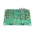
EVM Layout
The overall layout of the TPS2456EVM is shown in Figure 1. Channel A is the upper portion of the board
and Channel B is the midsection. The lower portion of the board contains the optional automatic retry on
fault circuitry.
Channel A
Pass
Mosfet
Channel A
OR-ing
Mosfet
Channel A
load
capacitors
Channel A
Output
TPS2456
Channel B
Output
Channel B
Pass
Mosfet
Channel B
OR-ing
Mosfet
Channel A
Retry
Circuit
Channel B
Retry
Circuit
Channel B
load
capacitors
Figure 1. TPS2456 General Layout
SLVU368 – March 2010
Submit Documentation Feedback
TPS2456EVM
Copyright © 2010, Texas Instruments Incorporated
1
�Connector and Jumper Description
2
www.ti.com
Connector and Jumper Description
J1
J2
J3
Channel A positive input supply voltage
Channel A hot swap positive output voltage
Shorting this jumper connects a 1kΩ resistor across the output of Channel A. This is useful to
discharge any output capacitance on Channel A.
J4–J7
Channel A Load Capacitors. Shorting each of these jumpers will add 220µF of capacitance
across the output of the board. A total of 880µF can be placed across the output using these
four jumpers.
J8
Channel A input supply voltage return (ground).
J9
Channel A output voltage return (ground)
J10
Current limit selection. Jumping pin 1 to pin 2 (EACH) sets the current limit of each channel to
8.36A. This could provide a total of 16.72A of current to the load if there is equal current
sharing between the two channels. Jumping pin 2 to pin 3 (TOTAL) sets the total maximum
current provided to the load to 8.36A.
J11
Channel B hot swap positive output voltage
J12
Channel B positive input supply voltage
J13
Shorting this jumper connects a 1kΩ resistor across the output of Channel B. This is useful to
discharge any output capacitance on Channel B.
J14–J17 Channel B Load Capacitors. Shorting each of these jumpers will add 220µF of capacitance
across the output of the board. A total of 880µF can be placed across the output using these
four jumpers
J18
Channel B output voltage return (ground)
J19
Channel B input supply voltage return (ground).
J20
Retry A: Shorting this jumper enables a channel retry function where the TPS2456 will attempt
to repower a Channel A after a fault has occurred. The TPS2456 will continuously retry until
the fault is removed. If the jumper is left open then the channel will be latched off when a fault
occurs.
J21
ENA: Shorting this jumper connects pin 31 (ENA) of the TPS2456 to ground thus disabling
Channel A of the TPS2456.
J22
Retry B: Shorting this jumper enables a channel retry function where the TPS2456 will attempt
to repower a Channel B after a fault has occurred. The TPS2456 will continuously retry until
the fault is removed. If the jumper is left open then the channel will be latched off when a fault
occurs.
J23
ENB: Shorting this jumper connects pin 29 (ENB) of the TPS2456 to ground thus disabling
Channel B of the TPS2456.
J24
ORENA: Shorting this jumper connects pin 6 (ORENA) of the TPS2456 to ground thus
disabling the OR-ing function. The board has a OR-ing transistor (Q2) installed in series with
the power path. Under normal conditions, this jumper should be left open to enable the OR-ing
transistor so current can flow to the output.
J25
ORENB: Shorting this jumper connects pin 14 (ORENB) of the TPS2456 to ground thus
disabling the OR-ing function. The board has a OR-ing transistor (Q4) installed in series with
the power path. Under normal conditions, this jumper should be left open to enable the OR-ing
transistor so current can flow to the output.
2
TPS2456EVM
SLVU368 – March 2010
Submit Documentation Feedback
Copyright © 2010, Texas Instruments Incorporated
�www.ti.com
Setup
3
Setup
3.1
Basic Setup
Figure 1 shows the basic setup for performance bench testing using resistive loads on channel A. Channel
B can be configured the same way as well if dual channel testing is desired. In this set-up, the on board
capacitors (C4–C7) can be used to supply a capacitive load to check the output voltage ramp. A load can
be connected to the output of the TPS2456EVM as shown.
POWER +12V
SUPPLY 1 GND
V Meter
LOAD 1
During the output voltage ramp-up, the current drawn from the input power supply is equal to the current
in the resistor plus the current required to charge the capacitance. The total current available for the
resistor and capacitors is fixed by the current limit of the TPS2456 which is set to a nominal 8.36A on the
EVM board. The 8.36A of available current must charge the capacitor and resistor combination up to 12V
before the fault timer expires. The fault timer is set to a nominal 2.97ms on the EVM board. This means
there is a minimum resistance value (maximum current draw) for the load for each selected output
capacitance value. Any lower resistance draws too much current and triggers the fault timer. The minimum
resistance value, based on nominal or typical circuit values, that can be supported is:
Output Capacitance
Load Resistance
220 µF
>1.43 Ω
440 µF
>1.46 Ω
660 µF
>1.56 Ω
880 µF
>1.78 Ω
Each channel of the TPS2456EVM can be independently enabled. Each channel can also be configured
to latch-off during a fault or to periodically retry starting. The retry and enable functions are configured
using shunts on two pin jumper headers. The functionality of these jumpers is:
J21
J20
OPEN
OPEN
OPEN
SHORT
Function
Channel A Enabled, Latch off on fault
Channel A Enabled, Retry on fault
SHORT
OPEN
Channel A Disabled
SHORT
SHORT
Channel A Disabled
J23
J22
Function
OPEN
OPEN
OPEN
SHORT
Channel B Enabled, Latch off on fault
SHORT
OPEN
Channel B Disabled
SHORT
SHORT
Channel B Disabled
Channel B Enabled, Retry on fault
SLVU368 – March 2010
Submit Documentation Feedback
TPS2456EVM
Copyright © 2010, Texas Instruments Incorporated
3
�Setup
3.2
www.ti.com
Alternate Configurations
+V
POWER +12V
SUPPLY 1 GND
GND
GND
GND
POWER
SUPPLY 2
LOAD 1
LOAD 2
+V
+12V
Figure 2. Dual Channel
Jumper Configurations:
J20 and J22 Jump to enable the retry on fault option for each respective channel. Leave open to latch
channel off on fault.
J24 and J25: leave open to enable the OR-ing transistors. The OR-ing transistors are not required for this
application, but are installed on the board; and therefore, must be enabled. J10 jump pin 1 to pin 2 (Each).
Each channel has individual peak current limit.
+12V
POWER +12V
SUPPLY 1 GND
+V
LOAD 1
GND
GND
GND
GND
LOAD 2
+12V
+V
Figure 3. Two Protected Loads
Jumper configurations:
J20 and J22 Jump to enable the retry on fault option for each respective channel. Leave open to latch
channel off on fault.
J24 and J25: leave open to enable the OR-ing transistors. The OR-ing transistors are not required for this
application, but are installed on the board; and therefore, must be enabled.
J10 jump pin 1 to pin 2 (Each). Each channel has individual peak current limit which protects the loads
from overcurrent. The input supply must be capable of providing current equal to 2 times the current limit
of a single channel. If the input power source rather than the loads needs to be protected from overcurrent
then jump pin 2 to pin 3 on J10 (Total). The total current draw from the input power supply is limited to the
peak current limit.
4
TPS2456EVM
SLVU368 – March 2010
Submit Documentation Feedback
Copyright © 2010, Texas Instruments Incorporated
�Setup
www.ti.com
+12V
POWER +12V
SUPPLY 1 GND
+V
LOAD 1
GND
GND
GND
GND
POWER
SUPPLY 2 +12V
+12V
Figure 4. Redundant Power Supply
Jumper Configurations:
J20 and J22 Jump to enable the retry on fault option for each respective channel. Leave open to latch
channel off on fault.
J24 and J25: leave open to enable the OR-ing transistors. The OR-ing transistors must be used in this
configuration to prevent cross current conduction between input power sources.
J10 jump pin 1 to pin 2 (Each). Each channel has individual peak current limit which protects the input
supplies from overcurrent conditions. The load can draw up to 2 times the current limit of a single channel
in this configuration. If the load rather than the input power source needs to be protected from overcurrent
then jump pin 2 to pin 3 on J10 (Total). The total current draw from the input power supply flowing to the
load is limited to the peak current limit. Note the OR-ing fets act as diodes so current sharing is not
ensured.
SLVU368 – March 2010
Submit Documentation Feedback
TPS2456EVM
Copyright © 2010, Texas Instruments Incorporated
5
�Schematic, PCB Layout and Bill of Materials
www.ti.com
Schematic, PCB Layout and Bill of Materials
4.1
Schematic
1
1
+
1
+
1
1
1
1
1
1
+
+
+
+
+
+
+
+
4
Figure 5. TPS2456 Schematic
6
TPS2456EVM
SLVU368 – March 2010
Submit Documentation Feedback
Copyright © 2010, Texas Instruments Incorporated
�Schematic, PCB Layout and Bill of Materials
www.ti.com
Figure 6. TPS2456 Schematic
SLVU368 – March 2010
Submit Documentation Feedback
TPS2456EVM
Copyright © 2010, Texas Instruments Incorporated
7
�Schematic, PCB Layout and Bill of Materials
4.2
www.ti.com
PCB Layout
Figure 7. TPS2456 Top Layer Assembly
Figure 8. TPS2456 Top Layer Routing
8
TPS2456EVM
SLVU368 – March 2010
Submit Documentation Feedback
Copyright © 2010, Texas Instruments Incorporated
�www.ti.com
Schematic, PCB Layout and Bill of Materials
Figure 9. TPS2456 Layer 2 Routing
Figure 10. TPS2456 Layer 3 Routing
SLVU368 – March 2010
Submit Documentation Feedback
TPS2456EVM
Copyright © 2010, Texas Instruments Incorporated
9
�Schematic, PCB Layout and Bill of Materials
www.ti.com
Figure 11. TPS2456 Layer 4 Routing
Figure 12. TPS2456 Layer 5 Routing
10
TPS2456EVM
SLVU368 – March 2010
Submit Documentation Feedback
Copyright © 2010, Texas Instruments Incorporated
�www.ti.com
Schematic, PCB Layout and Bill of Materials
Figure 13. TPS2456 Bottom Layer Routing
SLVU368 – March 2010
Submit Documentation Feedback
TPS2456EVM
Copyright © 2010, Texas Instruments Incorporated
11
�Schematic, PCB Layout and Bill of Materials
4.3
www.ti.com
Bill of Materials
Table 1. TPS2456 BOM
COUNT
RefDes
Value
Description
Size
Part Number
Mfr
2
C1, C18
1 uF
Capacitor, Ceramic, 25V, X7R, 20%
0805
Std.
Std.
2
C2, C19
47 uF
Capacitor, Aluminum, SM, 25V, ±20%
Case D
EEE-FK1E470P
Panasonic
2
C22, C24
1uF
Capacitor, Ceramic, 16V, X5R, 10%
0603
Std.
muRata
2
C23, C25
22uF
Capacitor, Ceramic, 16V, X5R, 10%
1206
Std.
muRata
0
C26, C27
Open
Capacitor, Ceramic, 25V
0603
Std.
muRata
5
C3, C10, C11, C13,
C21
0.1 uF
Capacitor, Ceramic, 25V, X7R, 20%
0805
Std.
Std.
8
C4, C5, C6, C7,
C14, C15, C16, C17
220 uF
Capacitor, Aluminum, SM, 25V, ±20%
Case F
EEE-FK1E221P
Panasonic
0
C8, C20
Open
Capacitor, Ceramic, 25V, X7R, 20%
0805
Std.
Std.
2
C9, C12
0.022 uF
Capacitor, Ceramic, 10V, X7R, 10%
0805
Std.
Std.
2
D1, D6
MBRM140
Diode, Schottky, 1A, 40V
457-04
MBRM140G
On Semi
2
D2, D5
BZD27C15P
"Diode, Zener, 15 V @ 50 mA,
,800 mW max., Pzsm = 300 W"
D0-219AB
BZD27C15P
Vishay
2
D3, D4
LTST-C155KGJRKT
Diode, Dual LED, Water Clear, 80-mA,
35/25-mcd
0.126 X 0.106 inch
LTST-C155KGJRKT
Lite On
8
J1, J2, J8, J9, J11,
J12, J18, J19
Jack, Banana, Non-ins., PC Mount
TH
3267
Pomona
1
J10
PEC03SAAN
Header, Male 3-pin, 100mil spacing,
0.100 inch x 3
PEC03SAAN
Sullins
16
J3, J4, J5, J6, J7,
J13, J14, J15, J16,
J17, J20, J21, J22,
J23, J24, J25
PEC02SAAN
Header, 2-pin, 100-mil spacing
0.100 in. x 2
PEC02SAAN
Sullins
4
Q1, Q2, Q3, Q4
CSD16403Q5
MOSFET, NChan, 25V, 28A, 2.9 milliOhm
QFN5X6mm
CSD16403Q5
TI
1
Q5
BSS84DW
MOSFET, Dual Pch, 50V, 130 mA
SC-70
BSS84DW-7-F
Diodes
1
Q6
SI1972DH
MOSFET, Dual Nch, 30V, 1.3A, 190
milliOhms,
SC-70
SI1972DH-TI-E3
Vishay
2
R1, R15
0.005
Resistor, Metal Strip, 1 W, 1%
2512
WSL25125L000FEA
Vishay-Dale
2
R17, R21
10k
Resistor, Chip, 1/16W, 1%
0603
Std.
Vishay
2
R18, R22
249k
Resistor, Chip, 1/16W, 1%
0603
Std.
Vishay
2
R19, R23
4.99k
Resistor, Chip, 1/16W, 1%
0603
Std.
Vishay
0
R2, R16, R25, R26
Open
Resistor, Chip, 1/16W, 1%
0603
Std.
Vishay
2
R20, R24
51.1k
Resistor, Chip, 1/16W, 1%
0603
Std.
Vishay
2
R3, R14
1K
Resistor, Chip, 1/2 W, 5%
2010
Std.
Std.
2
R4, R13
422
Resistor, Chip, 1/10 W, 1%
0805
Std.
Std.
4
R5, R6, R11, R12
100
Resistor, Chip, 1/16W, 1%
0603
Std.
Vishay
2
R7, R8
4.99k
Resistor, Chip, 1/10 W, 5%
0805
Std.
Std.
2
R9, R10
6.81K
Resistor, Chip, 1/16W, 1%
0603
Std.
Vishay
10
TP1, TP2, TP5, TP6,
TP7, TP8, TP9,
TP10, TP13, TP14
5012
Test Point, White, 0.062 in. Hole
TH
5012
Keystone
4
TP3, TP4, TP11,
TP12
5011
Test Point, Black, 0.062 in. Hole
TH
5011
Keystone
1
U1
TPS2456RHH
IC, Dual 12 V Hot Swap / ORing Controller
QFN-36
TPS2456RHH
TI
1
N/A
PCB, FR-4, 6-Layer, SMOBC, 4.830" x 5.070"
x .062"
HPA545**
Any
15
N/A
Shunt, Open-top
151-8000
Kobiconn
4
N/A
SPACER, Nylon, Hex, #6-32, 0.625"
14HTSP020
Eagle
4
N/A
SCREW, Nylon, Rnd Hd, #6-32, 0.25"
010632R025
Eagle
Notes: 1.
These assemblies must be clean and free from flux and all contaminants. Use of no clean flux is not acceptable.
2. These assemblies must comply with workmanship standards IPC-A-610 Class 2.
3. Ref designators marked with an asterisk ('**') cannot be substituted. All other components can be substituted with equivalent MFG's components.
4. If banana jacks (J1 - J2), (J8 - J9), (J11 - J12) and (J18 - J19) are supplied with solder lugs, dispose of lugs prior to installation on PCB. Solder lugs are NOT to be
installed on assembly.
12
TPS2456EVM
SLVU368 – March 2010
Submit Documentation Feedback
Copyright © 2010, Texas Instruments Incorporated
�Evaluation Board/Kit Important Notice
Texas Instruments (TI) provides the enclosed product(s) under the following conditions:
This evaluation board/kit is intended for use for ENGINEERING DEVELOPMENT, DEMONSTRATION, OR EVALUATION
PURPOSES ONLY and is not considered by TI to be a finished end-product fit for general consumer use. Persons handling the
product(s) must have electronics training and observe good engineering practice standards. As such, the goods being provided are
not intended to be complete in terms of required design-, marketing-, and/or manufacturing-related protective considerations,
including product safety and environmental measures typically found in end products that incorporate such semiconductor
components or circuit boards. This evaluation board/kit does not fall within the scope of the European Union directives regarding
electromagnetic compatibility, restricted substances (RoHS), recycling (WEEE), FCC, CE or UL, and therefore may not meet the
technical requirements of these directives or other related directives.
Should this evaluation board/kit not meet the specifications indicated in the User’s Guide, the board/kit may be returned within 30
days from the date of delivery for a full refund. THE FOREGOING WARRANTY IS THE EXCLUSIVE WARRANTY MADE BY
SELLER TO BUYER AND IS IN LIEU OF ALL OTHER WARRANTIES, EXPRESSED, IMPLIED, OR STATUTORY, INCLUDING
ANY WARRANTY OF MERCHANTABILITY OR FITNESS FOR ANY PARTICULAR PURPOSE.
The user assumes all responsibility and liability for proper and safe handling of the goods. Further, the user indemnifies TI from all
claims arising from the handling or use of the goods. Due to the open construction of the product, it is the user’s responsibility to
take any and all appropriate precautions with regard to electrostatic discharge.
EXCEPT TO THE EXTENT OF THE INDEMNITY SET FORTH ABOVE, NEITHER PARTY SHALL BE LIABLE TO THE OTHER
FOR ANY INDIRECT, SPECIAL, INCIDENTAL, OR CONSEQUENTIAL DAMAGES.
TI currently deals with a variety of customers for products, and therefore our arrangement with the user is not exclusive.
TI assumes no liability for applications assistance, customer product design, software performance, or infringement of
patents or services described herein.
Please read the User’s Guide and, specifically, the Warnings and Restrictions notice in the User’s Guide prior to handling the
product. This notice contains important safety information about temperatures and voltages. For additional information on TI’s
environmental and/or safety programs, please contact the TI application engineer or visit www.ti.com/esh.
No license is granted under any patent right or other intellectual property right of TI covering or relating to any machine, process, or
combination in which such TI products or services might be or are used.
FCC Warning
This evaluation board/kit is intended for use for ENGINEERING DEVELOPMENT, DEMONSTRATION, OR EVALUATION
PURPOSES ONLY and is not considered by TI to be a finished end-product fit for general consumer use. It generates, uses, and
can radiate radio frequency energy and has not been tested for compliance with the limits of computing devices pursuant to part 15
of FCC rules, which are designed to provide reasonable protection against radio frequency interference. Operation of this
equipment in other environments may cause interference with radio communications, in which case the user at his own expense
will be required to take whatever measures may be required to correct this interference.
EVM Warnings and Restrictions
It is important to operate this EVM within the input voltage range of 8.5 V to 15 V and the output voltage range of 8.5 V to 15 V .
Exceeding the specified input range may cause unexpected operation and/or irreversible damage to the EVM. If there are
questions concerning the input range, please contact a TI field representative prior to connecting the input power.
Applying loads outside of the specified output range may result in unintended operation and/or possible permanent damage to the
EVM. Please consult the EVM User's Guide prior to connecting any load to the EVM output. If there is uncertainty as to the load
specification, please contact a TI field representative.
During normal operation, some circuit components may have case temperatures greater than 85°C. The EVM is designed to
operate properly with certain components above 85°C as long as the input and output ranges are maintained. These components
include but are not limited to linear regulators, switching transistors, pass transistors, and current sense resistors. These types of
devices can be identified using the EVM schematic located in the EVM User's Guide. When placing measurement probes near
these devices during operation, please be aware that these devices may be very warm to the touch.
Mailing Address: Texas Instruments, Post Office Box 655303, Dallas, Texas 75265
Copyright © 2010, Texas Instruments Incorporated
�IMPORTANT NOTICE
Texas Instruments Incorporated and its subsidiaries (TI) reserve the right to make corrections, modifications, enhancements, improvements,
and other changes to its products and services at any time and to discontinue any product or service without notice. Customers should
obtain the latest relevant information before placing orders and should verify that such information is current and complete. All products are
sold subject to TI’s terms and conditions of sale supplied at the time of order acknowledgment.
TI warrants performance of its hardware products to the specifications applicable at the time of sale in accordance with TI’s standard
warranty. Testing and other quality control techniques are used to the extent TI deems necessary to support this warranty. Except where
mandated by government requirements, testing of all parameters of each product is not necessarily performed.
TI assumes no liability for applications assistance or customer product design. Customers are responsible for their products and
applications using TI components. To minimize the risks associated with customer products and applications, customers should provide
adequate design and operating safeguards.
TI does not warrant or represent that any license, either express or implied, is granted under any TI patent right, copyright, mask work right,
or other TI intellectual property right relating to any combination, machine, or process in which TI products or services are used. Information
published by TI regarding third-party products or services does not constitute a license from TI to use such products or services or a
warranty or endorsement thereof. Use of such information may require a license from a third party under the patents or other intellectual
property of the third party, or a license from TI under the patents or other intellectual property of TI.
Reproduction of TI information in TI data books or data sheets is permissible only if reproduction is without alteration and is accompanied
by all associated warranties, conditions, limitations, and notices. Reproduction of this information with alteration is an unfair and deceptive
business practice. TI is not responsible or liable for such altered documentation. Information of third parties may be subject to additional
restrictions.
Resale of TI products or services with statements different from or beyond the parameters stated by TI for that product or service voids all
express and any implied warranties for the associated TI product or service and is an unfair and deceptive business practice. TI is not
responsible or liable for any such statements.
TI products are not authorized for use in safety-critical applications (such as life support) where a failure of the TI product would reasonably
be expected to cause severe personal injury or death, unless officers of the parties have executed an agreement specifically governing
such use. Buyers represent that they have all necessary expertise in the safety and regulatory ramifications of their applications, and
acknowledge and agree that they are solely responsible for all legal, regulatory and safety-related requirements concerning their products
and any use of TI products in such safety-critical applications, notwithstanding any applications-related information or support that may be
provided by TI. Further, Buyers must fully indemnify TI and its representatives against any damages arising out of the use of TI products in
such safety-critical applications.
TI products are neither designed nor intended for use in military/aerospace applications or environments unless the TI products are
specifically designated by TI as military-grade or "enhanced plastic." Only products designated by TI as military-grade meet military
specifications. Buyers acknowledge and agree that any such use of TI products which TI has not designated as military-grade is solely at
the Buyer's risk, and that they are solely responsible for compliance with all legal and regulatory requirements in connection with such use.
TI products are neither designed nor intended for use in automotive applications or environments unless the specific TI products are
designated by TI as compliant with ISO/TS 16949 requirements. Buyers acknowledge and agree that, if they use any non-designated
products in automotive applications, TI will not be responsible for any failure to meet such requirements.
Following are URLs where you can obtain information on other Texas Instruments products and application solutions:
Products
Applications
Amplifiers
amplifier.ti.com
Audio
www.ti.com/audio
Data Converters
dataconverter.ti.com
Automotive
www.ti.com/automotive
DLP® Products
www.dlp.com
Communications and
Telecom
www.ti.com/communications
DSP
dsp.ti.com
Computers and
Peripherals
www.ti.com/computers
Clocks and Timers
www.ti.com/clocks
Consumer Electronics
www.ti.com/consumer-apps
Interface
interface.ti.com
Energy
www.ti.com/energy
Logic
logic.ti.com
Industrial
www.ti.com/industrial
Power Mgmt
power.ti.com
Medical
www.ti.com/medical
Microcontrollers
microcontroller.ti.com
Security
www.ti.com/security
RFID
www.ti-rfid.com
Space, Avionics &
Defense
www.ti.com/space-avionics-defense
RF/IF and ZigBee® Solutions www.ti.com/lprf
Video and Imaging
www.ti.com/video
Wireless
www.ti.com/wireless-apps
Mailing Address: Texas Instruments, Post Office Box 655303, Dallas, Texas 75265
Copyright © 2010, Texas Instruments Incorporated
�