Order
Now
Product
Folder
Support &
Community
Tools &
Software
Technical
Documents
Reference
Design
TPS2513, TPS2513A, TPS2514, TPS2514A
SLVSBY8D – MAY 2013 – REVISED JUNE 2020
TPS251xx USB Dedicated Charging Port Controller
1 Features
3 Description
•
The TPS251xx devices are USB dedicated charging
port (DCP) controllers. An auto-detect feature
monitors USB data line voltage, and automatically
provides the correct electrical signatures on the data
lines to charge compliant devices among the
following dedicated charging schemes:
1. Divider 1 DCP, required to apply 2 V and 2.7 V
on the D+ and D– Lines respectively (TPS2513,
TPS2514)
2. Divider 2 DCP, required to apply 2.7 V and 2 V
on the D+ and D– Lines respectively (TPS2513,
TPS2514)
3. Divider 3 DCP, required to apply 2.7 V and 2.7 V
on the D+ and D– Lines respectively (TPS2513A,
TPS2514A)
4. BC1.2 DCP, required to short the D+ Line to the
D– Line
5. Chinese Telecom Standard YD/T 1591-2009
Shorted Mode, required to short the D+ Line to
the D– Line
6. 1.2 V on both D+ and D– Lines
1
•
•
•
•
•
•
•
•
•
Supports USB DCP shorting D+ line to
D– line per USB battery charging specification,
revision 1.2 (BC1.2)
Supports shorted mode (shorting D+ line to D–
line) per Chinese Telecommunication Industry
Standard YD/T 1591-2009
Supports USB DCP applying 2.7 V on D+ Line
and 2 V on D- line (or USB DCP applying
2 V on D+ line and 2.7 V on D– line) (TPS2513,
TPS2514)
Supports USB DCP applying 2.7 V on D+ line and
2.7 V on D- line (TPS2513A, TPS2514A)
Supports USB DCP applying 1.2 V on
D+ and D– Lines
Automatically Switch D+ and D– Lines
Connections for an Attached Device
Dual USB Port Controller
(TPS2513, TPS2513A)
Single USB port controller
(TPS2514, TPS2514A)
Operating range: 4.5 V to 5.5 V
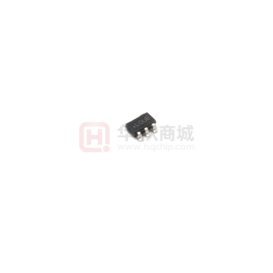
Available in SOT23-6 package
Device Information(1)
PART NUMBER
TPS2513, TPS2514
2 Applications
•
•
•
PACKAGE
SOT-23 (6)
BODY SIZE (NOM)
2.90 mm x 1.60 mm
(1) For all available packages, see the orderable addendum at
the end of the datasheet.
Vehicle USB power chargers
AC-DC adapters with USB ports
Other USB chargers
VBUS
TPS2561A
IN
0.1µF
5V
Power
GND
DP1
TPS2513
DM2
GND
GND
DM1
DD+
DP2
VBUS
DD+
GND
USB Connector2
VBUS
USB Connector1
Simplified Schematic
1
An IMPORTANT NOTICE at the end of this data sheet addresses availability, warranty, changes, use in safety-critical applications,
intellectual property matters and other important disclaimers. PRODUCTION DATA.
�TPS2513, TPS2513A, TPS2514, TPS2514A
SLVSBY8D – MAY 2013 – REVISED JUNE 2020
www.ti.com
Table of Contents
1
2
3
4
5
6
7
8
Features ..................................................................
Applications ...........................................................
Description .............................................................
Revision History.....................................................
Device Options.......................................................
Pin Configuration and Functions .........................
Specifications.........................................................
1
1
1
2
3
4
5
7.1
7.2
7.3
7.4
7.5
7.6
5
5
5
5
6
7
Absolute Maximum Ratings ......................................
ESD Ratings..............................................................
Recommended Operating Conditions.......................
Thermal Information ..................................................
Electrical Characteristics...........................................
Typical Characteristics ..............................................
Detailed Description .............................................. 9
8.1 Overview ................................................................... 9
8.2 Functional Block Diagrams ..................................... 10
8.3 Feature Description................................................. 11
8.4 Device Functional Modes........................................ 12
9
Applications and Implementation ...................... 13
9.1 Application Information............................................ 13
9.2 Typical Applications ................................................ 13
10 Power Supply Recommendations ..................... 15
11 Layout................................................................... 15
11.1 Layout Guidelines ................................................. 15
11.2 Layout Example .................................................... 15
12 Device and Documentation Support ................. 16
12.1
12.2
12.3
12.4
12.5
12.6
Related Links ........................................................
Receiving Notification of Documentation Updates
Support Resources ...............................................
Trademarks ...........................................................
Electrostatic Discharge Caution ............................
Glossary ................................................................
16
16
16
16
16
16
13 Mechanical, Packaging, and Orderable
Information ........................................................... 16
4 Revision History
NOTE: Page numbers for previous revisions may differ from page numbers in the current version.
Changes from Revision C (December 2016) to Revision D
Page
•
Changed DIVIDER 2 From: (D+/D– = 2 V/2.7 V) To: (D+/D– = 2.7V / 2V) in the Device Options table ............................... 3
•
Changed DIVIDER 3 From: (D+/D– = 2 V/2.7 V) To: (D+/D– = 2.7 V/2.7 V) in the Device Options table ............................ 3
•
Added title to Device Options table ........................................................................................................................................ 3
Changes from Revision B (September 2013) to Revision C
Page
•
Added ESD Rating table, Feature Description section, Device Functional Modes, Application and Implementation
section, Power Supply Recommendations section, Layout section, Device and Documentation Support section, and
Mechanical, Packaging, and Orderable Information section .................................................................................................. 1
•
Changed DM1 output voltage parameter symbol in Electrical Characteristics From: VDM1_2V To: VDM1_2.7V .......................... 6
•
Changed DM2 output voltage parameter symbol in Electrical Characteristics From: VDM2_2V To: VDM2_2.7V .......................... 6
Changes from Revision A (May 2013) to Revision B
Page
•
Added TPS2513A and TPS2514A devices throughout data sheet........................................................................................ 1
•
Changed Feature list to specify TPS251, TPS2513A, TPS2514, and TPS2514A devices ................................................... 1
•
Changed list of charging scheme items in Description........................................................................................................... 1
•
Changed Divider Mode section of the ELECTRICAL CHARACTERISTICS table to show values for the different devices . 6
•
Changed Functional Block Diagram for TPS2513, TPS2513A ............................................................................................ 10
•
Changed Functional Block Diagram for TPS2514, TPS2514A ............................................................................................ 10
•
Changed section title From: Divider 1 (DCP Applying 2 V on D+ Line and 2.7 V on D– Line) or Divider 2 (DCP
Applying 2.7 V on D+ Line and 2 V on D– Line) To: Divider DCP ....................................................................................... 11
•
Changed text in the Divider DCP paragraph ........................................................................................................................ 11
•
Added Divider 3 DCP image................................................................................................................................................. 11
•
Changed the DCP Auto-Detect section ................................................................................................................................ 12
2
Submit Documentation Feedback
Copyright © 2013–2020, Texas Instruments Incorporated
Product Folder Links: TPS2513 TPS2513A TPS2514 TPS2514A
�TPS2513, TPS2513A, TPS2514, TPS2514A
www.ti.com
SLVSBY8D – MAY 2013 – REVISED JUNE 2020
5 Device Options
Table 1. Device Options
CHARGING SCHEMES (DCP_AUTO)
DEVICE
(1)
NUMBER OF
CONTROLLER
DIVIDER 1
(D+/D– = 2 V/2.7 V)
DIVIDER 2
(D+/D– = 2.7V / 2V)
DIVIDER 3
(D+/D– = 2.7 V/2.7 V)
No
TPS2513
Dual
Yes (1)
Yes
TPS2514
Single
Yes (1)
Yes
No
TPS2513A
Dual
No
No
Yes
TPS2514A
Single
No
No
Yes
1.2-V MODE
(D+/D– SHORTED AND
BIAS TO 1.2 V)
BC1.2 AND YD/T
1591-2009 MODE
(D+/D– SHORTED)
Yes
Yes
See Figure 16
Copyright © 2013–2020, Texas Instruments Incorporated
Submit Documentation Feedback
Product Folder Links: TPS2513 TPS2513A TPS2514 TPS2514A
3
�TPS2513, TPS2513A, TPS2514, TPS2514A
SLVSBY8D – MAY 2013 – REVISED JUNE 2020
www.ti.com
6 Pin Configuration and Functions
TPS2513x DBV Package
6-Pin SOT-23
Top View
DP1
1
6
DM1
GND
2
5
IN
DP2
3
4
DM2
Not to scale
Pin Functions: TPS2513x
PIN
NO.
NAME
TYPE (1)
DESCRIPTION
1
DP1
I/O
Connected to the D+ or D– line of USB connector, provide the correct voltage with attached portable equipment for DCP
detection.
2
GND
G
Ground connection
3
DP2
I/O
Connected to the D+ or D– line of USB connector, provide the correct voltage with attached portable equipment for DCP
detection.
4
DM2
I/O
Connected to the D+ or D– line of USB connector, provide the correct voltage with attached portable equipment for DCP
detection.
5
IN
P
6
DM1
I/O
(1)
Power supply. Connect a ceramic capacitor with a value of 0.1-µF or greater from the IN pin to GND as close to the device
as possible.
Connected to the D+ or D– line of USB connector, provide the correct voltage with attached portable equipment for DCP
detection.
G = Ground, I = Input, O = Output, P = Power
TPS2514x DBV Package
6-Pin SOT-23
Top View
DP1
1
6
DM1
GND
2
5
IN
N/C
3
4
N/C
Not to scale
Pin Functions: TPS2514x
PIN
NO.
NAME
TYPE
(1)
DESCRIPTION
I/O
Connected to the D+ or D– line of USB connector, provide the correct voltage with attached portable equipment for
DCP detection.
GND
G
Ground connection
N/C
—
No connect pin. Can be grounded or left floating.
4
N/C
—
No connect pin. Can be grounded or left floating.
5
IN
P
Power supply. Connect a ceramic capacitor with a value of 0.1-µF or greater from the IN pin to GND as close to the
device as possible.
6
DM1
I/O
Connected to the D+ or D– line of USB connector, provide the correct voltage with attached portable equipment for
DCP detection.
1
DP1
2
3
(1)
4
G = Ground, I = Input, O = Output, P = Power
Submit Documentation Feedback
Copyright © 2013–2020, Texas Instruments Incorporated
Product Folder Links: TPS2513 TPS2513A TPS2514 TPS2514A
�TPS2513, TPS2513A, TPS2514, TPS2514A
www.ti.com
SLVSBY8D – MAY 2013 – REVISED JUNE 2020
7 Specifications
7.1 Absolute Maximum Ratings
over operating free-air temperature range (unless otherwise noted) (1)
Voltage
MIN
MAX
IN
–0.3
7
DP1, DP2 output voltage, DM1, DM2 output voltage
–0.3
5.8
DP1, DP2 input voltage, DM1, DM2 input voltage
–0.3
5.8
Continuous output sink current (DP1, DP2 input current, DM1, DM2 input current)
Continuous output source current ( DP1, DP2 output current, DM1, DM2 output current)
UNIT
V
35
mA
35
mA
Operating junction temperature, TJ
–40
125
°C
Storage temperature, Tstg
–65
150
°C
(1)
Stresses beyond those listed under Absolute Maximum Ratings may cause permanent damage to the device. These are stress ratings
only, which do not imply functional operation of the device at these or any other conditions beyond those indicated under Recommended
Operating Conditions. Exposure to absolute-maximum-rated conditions for extended periods may affect device reliability.
7.2 ESD Ratings
VALUE
V(ESD)
(1)
(2)
Electrostatic
discharge
Human-body model (HBM), per ANSI/ESDA/JEDEC JS-001 (1)
Pin 5
±2000
Pins 1, 3, 4, 6
±6000
Charged-device model (CDM), per JEDEC specification JESD22-C101 (2)
UNIT
V
±500
JEDEC document JEP155 states that 500-V HBM allows safe manufacturing with a standard ESD control process.
JEDEC document JEP157 states that 250-V CDM allows safe manufacturing with a standard ESD control process.
7.3 Recommended Operating Conditions
Voltages are referenced to GND (unless otherwise noted), positive current are into pins.
MIN
MAX
4.5
5.5
V
DP1 data line input voltage
0
5.5
V
DM1 data line input voltage
0
5.5
V
Continuous sink or source current
±10
mA
IDM1
Continuous sink or source current
±10
mA
VDP2
DP2 data line input voltage
0
5.5
V
VDM2
DM2 data line input voltage
0
5.5
V
IDP2
Continuous sink or source current
±10
mA
IDM2
Continuous sink or source current
±10
mA
TJ
Operating junction temperature
125
°C
VIN
Input voltage of IN
VDP1
VDM1
IDP1
–40
UNIT
7.4 Thermal Information
TPS2513x, TPS2514x
THERMAL METRIC (1)
DBV (SOT-23)
UNIT
6 PINS
RθJA
Junction-to-ambient thermal resistance
179.9
°C/W
RθJC(top)
Junction-to-case (top) thermal resistance
117.5
°C/W
RθJB
Junction-to-board thermal resistance
41.9
°C/W
ψJT
Junction-to-top characterization parameter
17.2
°C/W
ψJB
Junction-to-board characterization parameter
41.5
°C/W
RθJC(bot)
Junction-to-case (bottom) thermal resistance
—
°C/W
(1)
For more information about traditional and new thermal metrics, see the IC Package Thermal Metrics application report.
Copyright © 2013–2020, Texas Instruments Incorporated
Submit Documentation Feedback
Product Folder Links: TPS2513 TPS2513A TPS2514 TPS2514A
5
�TPS2513, TPS2513A, TPS2514, TPS2514A
SLVSBY8D – MAY 2013 – REVISED JUNE 2020
www.ti.com
7.5 Electrical Characteristics
Conditions are –40°C ≤ (TJ = TA) ≤ 125°C and 4.5 V ≤ VIN ≤ 5.5 V. Positive current are into pins. Typical values are at 25°C.
All voltages are with respect to GND (unless otherwise noted).
PARAMETER
TEST CONDITIONS
MIN
TYP
MAX
4.1
4.3
UNIT
UNDERVOLTAGE LOCKOUT
VUVLO
IN rising UVLO threshold voltage
3.9
Hysteresis (1)
100
V
mV
SUPPLY CURRENT
IIN
IN supply current
4.5 V ≤ V IN ≤ 5.5 V
155
200
µA
BC 1.2 DCP MODE (SHORT MODE)
RDPM_SHORT1
DP1 and DM1 shorting resistance
VDP1 = 0.8 V, IDM1 = 1 mA
RDCHG_SHORT1
Resistance between DP1/DM1 and GND
VDP1 = 0.8 V
VDPL_TH_DETACH1
Voltage threshold on DP1 (under which the
device goes back to divider mode)
157
200
Ω
350
656
1150
kΩ
310
330
350
mV
(1)
VDPL_TH_DETACH_HYS1
Hysteresis
50
RDPM_SHORT2
DP2 and DM2 shorting resistance
VDP2 = 0.8V, IDM2 = 1 mA
RDCHG_SHORT2
Resistance between DP2/DM2 and GND
VDP2 = 0.8 V
VDPL_TH_DETACH2
Voltage threshold on DP2 (under which the
device goes back to divider mode)
VDPL_TH_DETACH_HYS2
Hysteresis (1)
mV
157
200
Ω
350
656
1150
kΩ
310
330
350
mV
50
mV
DIVIDER MODE (TPS2513, TPS2514)
VDP1_2.7V
DP1 output voltage
VIN = 5 V
2.57
2.7
2.84
V
VDM1_2V
DM1 output voltage
VIN = 5 V
RDP1_PAD1
DP1 output impedance
IDP1 = –5 µA
1.9
2
2.1
V
24
30
36
kΩ
RDM1_PAD1
DM1 output impedance
IDM1 = –5 µA
24
VDP2_2.7V
DP2 output voltage
VIN = 5 V
2.57
30
36
kΩ
2.7
2.84
V
VDM2_2V
DM2 output voltage
VIN = 5 V
1.9
2
2.1
V
RDP2_PAD1
DP2 output impedance
IDP2 = –5 µA
24
30
36
kΩ
RDM2_PAD1
DM2 output impedance
IDM2 = –5 µA
24
30
36
kΩ
DIVIDER MODE (TPS2513A, TPS2514A)
VDP1_2.7V
DP1 output voltage
VIN = 5 V
2.57
2.7
2.84
V
VDM1_2.7V
DM1 output voltage
VIN = 5 V
2.57
2.7
2.84
V
RDP1_PAD1
DP1 output impedance
IDP1 = –5 µA
24
30
36
kΩ
RDM1_PAD1
DM1 output impedance
IDM1 = –5 µA
24
30
36
kΩ
VDP2_2.7V
DP2 output voltage
VIN = 5 V
2.57
2.7
2.84
V
VDM2_2.7V
DM2 output voltage
VIN = 5 V
2.57
2.7
2.84
V
RDP2_PAD1
DP2 output impedance
IDP2 = –5 µA
24
30
36
kΩ
RDM2_PAD1
DM2 output impedance
IDM2 = –5 µA
24
30
36
kΩ
VDP1_1.2V
DP1 output voltage
VIN = 5 V
1.12
1.2
1.28
V
VDM1_1.2V
DM1 output voltage
VIN = 5 V
1.12
1.2
1.28
V
RDM1_PAD2
DP1 output impedance
IDP1 = –5 µA
80
102
130
kΩ
RDP1_PAD2
DM1 output impedance
IDM1 = –5 µA
80
102
130
kΩ
VDP2_1.2V
DP2 output voltage
VIN = 5 V
1.12
1.2
1.28
V
VDM2_1.2V
DM2 output voltage
VIN = 5 V
1.12
1.2
1.28
V
RDP2_PAD2
DP2 output impedance
IDP2 = –5 µA
80
102
130
kΩ
RDM2_PAD2
DM2 output impedance
IDM2 = –5 µA
80
102
130
kΩ
1.2 V / 1.2 V MODE
(1)
6
Parameters provided for reference only, and do not constitute part of TI's published device specifications for purposes of TI's product
warranty.
Submit Documentation Feedback
Copyright © 2013–2020, Texas Instruments Incorporated
Product Folder Links: TPS2513 TPS2513A TPS2514 TPS2514A
�TPS2513, TPS2513A, TPS2514, TPS2514A
www.ti.com
SLVSBY8D – MAY 2013 – REVISED JUNE 2020
7.6 Typical Characteristics
6
6
V
VIN
IN
DM1
5
V
DVIN
IN
DM1
DP1
5
VIN, DM1, DP1 (V)
VIN, DM1, DP1 (V)
DP1
4
3
2
1
0
4
3
2
1
0
±1
±0.008
±0.006
±0.004
±0.002
0.000
0.002
Time (s)
±1
-0.04
0.004
0.06
0.08
0.1
C002
V
DVIN
IN
DM2
DM1
DP2
DP1
5
4
VIN, DM2, DP2 (V)
VIN, DM2, DP2 (V)
0.04
Figure 2. Power Off (DM1 and DP1)
3
2
1
0
4
3
2
1
0
±1
±0.008
±0.006
±0.004
±0.002
0.000
0.002
Time (s)
±1
-0.04
0.004
-0.02
0
0.02
0.04
0.06
0.08
Time (s)
C003
Figure 3. Power On (DM2 and DP2)
0.1
C004
Figure 4. Power Off (DM2 and DP2)
3.2
3.2
VIN = 5 V
DP2 and DM2 Output Voltage (V)
DP1 and DM1 Output Voltage (V)
0.02
6
VIN
VIN
DM2
DP2
5
0
Time (s)
Figure 1. Power On (DM1 and DP1)
6
-0.02
C001
2.8
2.4
2
DP1
V
DP1
V
DM1
DM1
1.6
±40
±20
0
20
40
60
80
TJ Junction Temperature (ƒC)
100
120
2.8
2.4
2
DP1
V
DP2
V
DM1
DM2
1.6
140
C005
Figure 5. DP1 and DM1 Output Voltage vs Temperature
Copyright © 2013–2020, Texas Instruments Incorporated
VIN = 5 V
±40
±20
0
20
40
60
80
100
120
TJ Junction Temperature (ƒC)
140
C006
Figure 6. DP2 and DM2 Output Voltage vs Temperature
Submit Documentation Feedback
Product Folder Links: TPS2513 TPS2513A TPS2514 TPS2514A
7
�TPS2513, TPS2513A, TPS2514, TPS2514A
SLVSBY8D – MAY 2013 – REVISED JUNE 2020
www.ti.com
Typical Characteristics (continued)
180
VIN = 5 V
Supply Current (µA)
170
160
150
140
130
±40
±20
0
20
40
60
80
100
120
TJ Junction Temperature (ƒC)
140
C007
Figure 7. Supply Current vs Temperature
8
Submit Documentation Feedback
Copyright © 2013–2020, Texas Instruments Incorporated
Product Folder Links: TPS2513 TPS2513A TPS2514 TPS2514A
�TPS2513, TPS2513A, TPS2514, TPS2514A
www.ti.com
SLVSBY8D – MAY 2013 – REVISED JUNE 2020
8 Detailed Description
8.1 Overview
The following overview references various industry standards. TI always recommends consulting the latest
standard to ensure the most recent and accurate information.
Rechargeable portable equipment requires an external power source to charge its batteries. USB ports are
convenient locations for charging because of an available 5-V power source. Universally accepted standards are
required to ensure host and client-side devices meet the power management requirements. Traditionally, USB
host ports following the USB 2.0 Specification must provide at least 500 mA to downstream client-side devices.
Because multiple USB devices can be attached to a single USB port through a bus-powered hub, it is the
responsibility of the client-side device to negotiate the power allotment from the host to ensure the total current
draw does not exceed 500 mA. In general, each USB device can subsequently request more current which is
granted in steps of 100 mA, up 500 mA total. The host may grant or deny the request based on the available
current.
Additionally, the success of the USB technology makes the micro-USB connector a popular choice for wall
adapter cables. This allows a portable device to charge from both a wall adapter and USB port with only one
connector.
One common difficulty has resulted from this. As USB charging has gained popularity, the 500-mA minimum
defined by the USB 2.0 Specification or 900 mA defined in the USB 3.0 Specification, has become insufficient for
many handsets, tablets and personal media players (PMP) which have a higher rated charging current. Wall
adapters and car chargers can provide much more current than 500 mA or 900 mA to fast charge portable
devices. Several new standards have been introduced defining protocol handshaking methods that allow host
and client devices to acknowledge and draw additional current beyond the 500 mA (defined in the USB 2.0
Specification) or 900 mA (defined in the USB 3.0 Specification) minimum while using a single micro-USB input
connector.
The devices support four of the most common protocols:
• USB Battery Charging Specification, Revision 1.2 (BC1.2)
• Chinese Telecommunications Industry Standard YD/T 1591-2009
• Divider mode
• 1.2 V on both D+ and D– lines
YD/T 1591-2009 is a subset of the BC1.2 specification supported by the vast majority of devices that implement
USB charging. Divider and 1.2-V charging schemes are supported in devices from specific yet popular device
makers. BC1.2 has three different port types, listed as follows.
• Standard downstream port (SDP)
• Charging downstream port (CDP)
• Dedicated charging port (DCP)
The BC1.2 Specification defines a charging port as a downstream facing USB port that provides power for
charging portable equipment.
Table 2 shows different port operating modes according to the BC1.2 Specification.
Table 2. Operating Modes
PORT TYPE
SUPPORTS USB 2.0
COMMUNICATION
MAXIMUM ALLOWABLE CURRENT
DRAWN BY PORTABLE EQUIPMENT (A)
SDP (USB 2.0)
Yes
0.5
SDP (USB 3.0)
Yes
0.9
CDP
Yes
1.5
DCP
No
1.5
Copyright © 2013–2020, Texas Instruments Incorporated
Submit Documentation Feedback
Product Folder Links: TPS2513 TPS2513A TPS2514 TPS2514A
9
�TPS2513, TPS2513A, TPS2514, TPS2514A
SLVSBY8D – MAY 2013 – REVISED JUNE 2020
www.ti.com
The BC1.2 Specification defines the protocol necessary to allow portable equipment to determine what type of
port it is connected to so that it can allot its maximum allowable current drawn. The hand-shaking process is two
steps. During step one, the primary detection, the portable equipment outputs a nominal 0.6-V output on its D+
line and reads the voltage input on its D– line. The portable device concludes it is connected to a SDP if the
voltage is less than the nominal data detect voltage of 0.3 V. The portable device concludes that it is connected
to a Charging Port if the D– voltage is greater than the nominal data detect voltage of 0.3 V and less than 0.8 V.
The second step, the secondary detection, is necessary for portable equipment to determine between a CDP and
a DCP. The portable device outputs a nominal 0.6-V output on its D– line and reads the voltage input on its D+
line. The portable device concludes it is connected to a CDP if the data line being remains is less than the
nominal data detect voltage of 0.3 V. The portable device concludes it is connected to a DCP if the data line
being read is greater than the nominal data detect voltage of 0.3 V and less than 0.8 V.
8.2 Functional Block Diagrams
S1
DM1
S2
IN
Auto-detect
S4
DP1
S3
2.7V
VDM1
1.2V
UVLO
S5
DM2
DRIVER
S6
S8
Auto-detect
GND
DP2
S7
2.7V
VDM2
1.2V
TPS2513: VDM1 / VDM2= 2 V
TPS2513A: VDM1 / VDM2= 2.7 V
Figure 8. Functional Block Diagram, TPS2513, TPS2513A
S1
DM1
IN
S2
UVLO
S4
Auto-detect
DP1
S3
DRIVER
2.7V
VDM1
1.2V
N/C
TPS2514: VDM1 = 2 V
TPS2514A: VDM1 = 2.7 V
N/C
GND
Figure 9. Functional Block Diagram, TPS2514, TPS2514A
10
Submit Documentation Feedback
Copyright © 2013–2020, Texas Instruments Incorporated
Product Folder Links: TPS2513 TPS2513A TPS2514 TPS2514A
�TPS2513, TPS2513A, TPS2514, TPS2514A
www.ti.com
SLVSBY8D – MAY 2013 – REVISED JUNE 2020
8.3 Feature Description
8.3.1 Dedicated Charging Port (DCP)
A dedicated charging port (DCP) is a downstream port on a device that outputs power through a USB connector
but is not capable of enumerating a downstream device, which generally allows portable devices to fast charge at
their maximum rated current. A USB charger is a device with a DCP, such as a wall adapter or car power
adapter. A DCP is identified by the electrical characteristics of its data lines. The following DCP identification
circuits are usually used to meet the handshaking detections of different portable devices.
8.3.2 Short the D+ Line to the D– Line
The USB BC1.2 Specification and the Chinese Telecommunications Industry Standard YD/T 1591-2009 define
that the D+ and D– data lines must be shorted together with a maximum series impedance of 200 Ω. This is
shown in Figure 10.
D200 Ω (max)
D+
GND
USB Connector
VBUS
5.0 V
Figure 10. DCP Short Mode
8.3.3 Divider DCP
There are three charging schemes for divider DCP. They are named after Divider 1, Divider 2, and Divider 3
DCPs that are shown in Figure 11, Figure 12, and Figure 13. The Divider 1 charging scheme is used for 5-W
adapters, and applies 2 V to the D+ line and 2.7 V to the D– data line. The Divider 2 charging scheme is used for
10-W adapters, and applies 2.7 V on the D+ line and 2 V is applied on the D– line. The Divider 3 charging
scheme is used for 12-W adapters, and applies 2.7 V on D+ and D– lines.
D+
2.7 V 2.0 V
GND
5.0 V
DD+
2.0 V 2.7 V
GND
Figure 11. Divider 1 DCP
Figure 12. Divider 2 DCP
VBUS
DD+
2.7 V 2.7 V
GND
USB Connector
D-
VBUS
5.0 V
USB Connector
VBUS
USB Connector
5.0 V
Figure 13. Divider 3 DCP
8.3.4 Applying 1.2 V to the D+ Line and 1.2 V to the D– Line
As shown in Figure 14, some tablet USB chargers require 1.2 V on the shorted data lines of the USB connector.
The maximum resistance between the D+ line and the D– line is 200 Ω.
D200 Ω (max)
1.2 V
D+
GND
USB Connector
VBUS
5.0 V
Figure 14. DCP Applying 1.2 V to the D+ Line and 1.2 V to the D– Line
The devices are USB dedicated charging port (DCP) controllers. Applications include vehicle power charger, wall
adapters with USB DCP and other USB chargers. The device DCP controllers have the auto-detect feature that
monitors the D+ and D– line voltages of the USB connector, providing the correct electrical signatures on the DP
and DM pins for the correct detections of compliant portable devices to fast charge. These portable devices
include smart phones, 5-V tablets and personal media players.
Copyright © 2013–2020, Texas Instruments Incorporated
Submit Documentation Feedback
Product Folder Links: TPS2513 TPS2513A TPS2514 TPS2514A
11
�TPS2513, TPS2513A, TPS2514, TPS2514A
SLVSBY8D – MAY 2013 – REVISED JUNE 2020
www.ti.com
Feature Description (continued)
8.3.5 DCP Auto-Detect
The devices integrate an auto-detect feature to support divider mode, short mode and 1.2 V / 1.2 V modes. If a
divider device is attached, 2.7 V is applied to the DP pin and 2 V is applied to the DM pin. If a BC1.2-compliant
device is attached, the TPS2513 and TPS2514 automatically switches into short mode. If a device compliant with
the 1.2 V / 1.2 V charging scheme is attached, 1.2 V is applied on both the DP pin and the DM pin. The
functional diagram of DCP auto-detect feature (DM1 and DP1) is shown in Figure 15. DCP auto-detect feature
(DM2 and DP2 of TPS2513) has the same functional configuration. For TPS2513A and TPS2514A, the devices
also have DCP auto-detect feature and the auto-detect have the same functional configuration expect for the
default mode is Divider 3 (D+/D– = 2.7 V / 2.7 V).
5V
S1
S2
DM1
D-
DP1
D+
S4
GND
S3
2.0V
2.7V
1.2 V
GND
USB Connector
VBUS
Divider 2
S1, S2: ON
S3, S4: OFF
Short Mode
S4 ON
S1, S2, S3: OFF
1.2V on DP1 and DM1
S3, S4: ON
S1, S2: OFF
TPS2513, TPS2514
Figure 15. TPS2513 and TPS2514 DCP Auto-Detect Functional Diagram
8.3.6 Undervoltage Lockout (UVLO)
The undervoltage lockout (UVLO) circuit disables DP1, DM1, DP2 and DM2 output voltage until the input voltage
reaches the UVLO turnon threshold. Built-in hysteresis prevents unwanted oscillations due to input voltage drop
from large current surges.
8.4 Device Functional Modes
The devices operate in DCP mode and automatically monitor the voltage of the USB data lines, and provide the
correct electronic signatures on the data lines to charge compliant devices.
12
Submit Documentation Feedback
Copyright © 2013–2020, Texas Instruments Incorporated
Product Folder Links: TPS2513 TPS2513A TPS2514 TPS2514A
�TPS2513, TPS2513A, TPS2514, TPS2514A
www.ti.com
SLVSBY8D – MAY 2013 – REVISED JUNE 2020
9 Applications and Implementation
NOTE
Information in the following applications sections is not part of the TI component
specification, and TI does not warrant its accuracy or completeness. TI’s customers are
responsible for determining suitability of components for their purposes. Customers should
validate and test their design implementation to confirm system functionality.
9.1 Application Information
The TPS251xx devices are USB dedicated charging port. The devices only provide the correct electrical
signatures on the data lines of USB charger port and do not provide any power for the VBUS. Below is typical
applications for USB charging ports.
9.2 Typical Applications
5.0 V
5.0 V
VBUS
GND
DM1
TPS2513, TPS2514
DD+
DP1
GND
Figure 16. 5-W USB Charger Application
USB Connector
D+
DP1
USB Connector
D-
DM1
TPS2513, TPS2514
VBUS
Figure 17. 10-W USB Charger Application
9.2.1 Design Requirements
Table 3 lists the design parameters for this example.
Table 3. Design Parameters
PARAMETER
VALUE
Input voltage, V(IN)
5V
Output voltage, V(DC)
5V
Maximum continuous output current, I(OUT)
2.5 A
9.2.2 Detailed Design Procedure
9.2.2.1 Divide Mode Selection of 5-W and 10-W USB Chargers
The TPS2513 and TPS2514 provide two types of connections between the DP pin and the DM pin and between
the D+ data line and the D– data line of the USB connector for a 5-W USB charger and a 10-W USB charger
with a single USB port. For 5-W USB charger, the DP1 pin is connected to the D– line and the DM1 pin is
connected to the D+ line. This is shown in Figure 16. For 10-W USB charger, the DP1 pin is connected to the D+
line and the DM1 pin is connected to the D– line. This is shown in Figure 17. Table 4 shows different charging
schemes for both 5-W and 10-W USB charger solutions. DP2 and DM2 of TPS2513 also provides this two types
of connections.
Table 4. Charging Schemes for 5-W And 10-W USB Chargers
USB CHARGER TYPE
CONTAINING CHARGING SCHEMES
5-W
Divider 1
1.2 V on both D+ and D– Lines
BC1.2 DCP
10-W
Divider 2
1.2 V on both D+ and D– Lines
BC1.2 DCP
Copyright © 2013–2020, Texas Instruments Incorporated
Submit Documentation Feedback
Product Folder Links: TPS2513 TPS2513A TPS2514 TPS2514A
13
�TPS2513, TPS2513A, TPS2514, TPS2514A
SLVSBY8D – MAY 2013 – REVISED JUNE 2020
www.ti.com
9.2.3 Application Curves
14
Figure 18. POWER ON (DM1 and DP1)
Figure 19. POWER OFF (DM1 and DP1)
Figure 20. POWER ON (DM2 and DP2)
Figure 21. POWER OFF (DM2 and DP2)
Submit Documentation Feedback
Copyright © 2013–2020, Texas Instruments Incorporated
Product Folder Links: TPS2513 TPS2513A TPS2514 TPS2514A
�TPS2513, TPS2513A, TPS2514, TPS2514A
www.ti.com
SLVSBY8D – MAY 2013 – REVISED JUNE 2020
10 Power Supply Recommendations
The devices are designed for a supply-voltage range of 4.5 V ≤ VIN ≤ 5.5 V. If the input supply is placed more
than a few inches from the device, an input ceramic bypass capacitor higher than 0.1 µF is recommended. The
undervoltage lockout (UVLO) circuit disables DP1, DM1, DP2, and DM2 output voltage until the input voltage
reaches the UVLO turnon threshold.
11 Layout
11.1 Layout Guidelines
Place the devices near the USB output connector and place the 0.1-µF bypass capacitor near the IN pin.
11.2 Layout Example
Figure 22. Layout Recommendation
Copyright © 2013–2020, Texas Instruments Incorporated
Submit Documentation Feedback
Product Folder Links: TPS2513 TPS2513A TPS2514 TPS2514A
15
�TPS2513, TPS2513A, TPS2514, TPS2514A
SLVSBY8D – MAY 2013 – REVISED JUNE 2020
www.ti.com
12 Device and Documentation Support
12.1 Related Links
The table below lists quick access links. Categories include technical documents, support and community
resources, tools and software, and quick access to sample or buy.
Table 5. Related Links
PARTS
PRODUCT FOLDER
SAMPLE & BUY
TECHNICAL
DOCUMENTS
TOOLS &
SOFTWARE
SUPPORT &
COMMUNITY
TPS2513
Click here
Click here
Click here
Click here
Click here
TPS2513A
Click here
Click here
Click here
Click here
Click here
TPS2514
Click here
Click here
Click here
Click here
Click here
TPS2514A
Click here
Click here
Click here
Click here
Click here
12.2 Receiving Notification of Documentation Updates
To receive notification of documentation updates, navigate to the device product folder on ti.com. In the upper
right corner, click on Alert me to register and receive a weekly digest of any product information that has
changed. For change details, review the revision history included in any revised document.
12.3 Support Resources
TI E2E™ support forums are an engineer's go-to source for fast, verified answers and design help — straight
from the experts. Search existing answers or ask your own question to get the quick design help you need.
Linked content is provided "AS IS" by the respective contributors. They do not constitute TI specifications and do
not necessarily reflect TI's views; see TI's Terms of Use.
12.4 Trademarks
E2E is a trademark of Texas Instruments.
All other trademarks are the property of their respective owners.
12.5 Electrostatic Discharge Caution
These devices have limited built-in ESD protection. The leads should be shorted together or the device placed in conductive foam
during storage or handling to prevent electrostatic damage to the MOS gates.
12.6 Glossary
SLYZ022 — TI Glossary.
This glossary lists and explains terms, acronyms, and definitions.
13 Mechanical, Packaging, and Orderable Information
The following pages include mechanical, packaging, and orderable information. This information is the most
current data available for the designated devices. This data is subject to change without notice and revision of
this document. For browser-based versions of this data sheet, refer to the left-hand navigation.
16
Submit Documentation Feedback
Copyright © 2013–2020, Texas Instruments Incorporated
Product Folder Links: TPS2513 TPS2513A TPS2514 TPS2514A
�PACKAGE OPTION ADDENDUM
www.ti.com
10-Dec-2020
PACKAGING INFORMATION
Orderable Device
Status
(1)
Package Type Package Pins Package
Drawing
Qty
Eco Plan
(2)
Lead finish/
Ball material
MSL Peak Temp
Op Temp (°C)
Device Marking
(3)
(4/5)
(6)
TPS2513ADBVR
ACTIVE
SOT-23
DBV
6
3000
RoHS & Green
NIPDAU
Level-1-260C-UNLIM
-40 to 125
PB2Q
TPS2513ADBVT
ACTIVE
SOT-23
DBV
6
250
RoHS & Green
NIPDAU
Level-1-260C-UNLIM
-40 to 125
PB2Q
TPS2513DBVR
ACTIVE
SOT-23
DBV
6
3000
RoHS & Green
NIPDAU
Level-1-260C-UNLIM
-40 to 125
2513
TPS2513DBVT
ACTIVE
SOT-23
DBV
6
250
RoHS & Green
NIPDAU
Level-1-260C-UNLIM
-40 to 125
2513
TPS2514ADBVR
ACTIVE
SOT-23
DBV
6
3000
RoHS & Green
NIPDAU
Level-1-260C-UNLIM
-40 to 125
PB3Q
TPS2514ADBVT
ACTIVE
SOT-23
DBV
6
250
RoHS & Green
NIPDAU
Level-1-260C-UNLIM
-40 to 125
PB3Q
TPS2514DBVR
ACTIVE
SOT-23
DBV
6
3000
RoHS & Green
NIPDAU
Level-1-260C-UNLIM
-40 to 125
2514
TPS2514DBVT
ACTIVE
SOT-23
DBV
6
250
RoHS & Green
NIPDAU
Level-1-260C-UNLIM
-40 to 125
2514
(1)
The marketing status values are defined as follows:
ACTIVE: Product device recommended for new designs.
LIFEBUY: TI has announced that the device will be discontinued, and a lifetime-buy period is in effect.
NRND: Not recommended for new designs. Device is in production to support existing customers, but TI does not recommend using this part in a new design.
PREVIEW: Device has been announced but is not in production. Samples may or may not be available.
OBSOLETE: TI has discontinued the production of the device.
(2)
RoHS: TI defines "RoHS" to mean semiconductor products that are compliant with the current EU RoHS requirements for all 10 RoHS substances, including the requirement that RoHS substance
do not exceed 0.1% by weight in homogeneous materials. Where designed to be soldered at high temperatures, "RoHS" products are suitable for use in specified lead-free processes. TI may
reference these types of products as "Pb-Free".
RoHS Exempt: TI defines "RoHS Exempt" to mean products that contain lead but are compliant with EU RoHS pursuant to a specific EU RoHS exemption.
Green: TI defines "Green" to mean the content of Chlorine (Cl) and Bromine (Br) based flame retardants meet JS709B low halogen requirements of