TPS2540, TPS2540A
TPS2541, TPS2541A
SLVSAG2C – OCTOBER 2010 – REVISED OCTOBER 2011
www.ti.com
USB Charging Port Power Switch and Controller
Check for Samples: TPS2540, TPS2540A, TPS2541, TPS2541A
FEATURES
DESCRIPTION
•
The TPS2540/40A and TPS2541/41A are a
combination of current-limited USB port power switch
with a USB 2.0 high-speed data line (D+/D-) switch
and a USB charging port identification circuit.
Applications include notebook PCs and other
intelligent USB host devices. The wide bandwidth (2.6
GHz) data-line switch also features low capacitance
and low on resistance, allowing signals to pass with
minimum edge and phase distortion. The
TPS2540/40A/41/41A monitors D+ and D-, providing
the correct hand-shaking protocol with compliant
client devices.
1
2
•
•
•
•
•
•
•
•
•
Meets Battery Charging Specification BC1.2
for DCP and CDP
Meets Chinese Telecommunications Industry
Standard YD/T 1591-2009
Supports Sleep-Mode Charging for Most
Available Apple® Devices and/or BC1.2
Compliant Devices
Compatible With USB 2.0 and 3.0 Power
Switch Requirements
2.6-GHz Bandwidth USB 2.0 Data Switch
73-mΩ (typ.) High-Side MOSFET
Adjustable Current Limit up to 2.8 A (typical)
OUT Discharge Through CTLx=000
(TPS2540/40A) or DSC (TPS2541/41A) Input
Longer Detach Detection Time (TPS2540A/41A)
Supporting Additional Legacy Devices
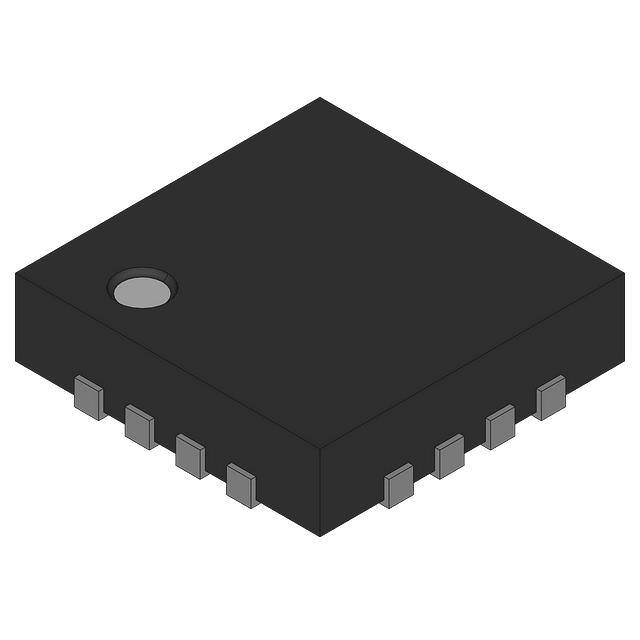
Available in 16-Pin QFN Package
APPLICATIONS
•
•
•
USB Ports/Hubs
Notebook PCs
Universal Wall Charging Adapter
The TPS2540/40A/41/41A supports the following
charging logic schemes:
• USB 2.0 BC1.2
• Chinese Telecom Standard YD/T 1591-2009
• Divider Mode, compliant with Apple devices such
as iPod® and iPhone®
CTL1-CTL3 logic inputs are used to select one of the
various charge modes provided by the TPS2540/40A
and TPS2541/41A. These charge modes allow the
host device to actively select between Dedicated
Charging Port (DCP) (wall-adapter emulation),
Charging Downstream Port (CDP) (active USB 2.0
data communications with 1.5-A support), or
Standard Downstream Port (SDP) USB 2.0 Mode
(active USB 2.0 data communications with 500-mA
support). The TPS2540/40A/41/41A also integrates
an auto-detect feature that supports both DCP
schemes for Battery Charging Specification (BC1.2)
and the Divider Mode without the need for outside
user interaction.
TPS2540/40A/41/41A RTE Package and Typical Application Diagram
To System Bus
ILIM0
ILIM1
GND
FAULT
TPS2540/40A/41/41A
RTE Package
(Top View)
16
15
14
13
4.5 V to 5.5 V
1
3
4
CUSB
VBUS
DD+
GND
ILIM0 16
RFAULT
10 kW
ILIM1 15
13 FAULT
2x
RILIM
ILIM Select
4
ILIM_SEL
10 DP_IN
Power Switch EN
5
EN/DSC
Mode Select I/O
6
CTL1
Mode Select I/O
7
CTL2
DM_OUT
2
Mode Select I/O
8
CTL3
DP_OUT
3
9
EN/DSC
5
6
7
GND 14
DM_IN
11
Exposed
Thermal Die
N/C
8
CTL3
DP_OUT
ILIM_SEL
OUT 12
12 OUT
CTL2
1
2
CTL1
IN
IN
0.1 mF
FAULT Signal
DM_OUT
To Peripheral
TPS2540/40A/41/41A
DM_IN 11
DP_IN 10
To Host Controller
UDG-10116
1
2
Please be aware that an important notice concerning availability, standard warranty, and use in critical applications of Texas
Instruments semiconductor products and disclaimers thereto appears at the end of this data sheet.
Apple, iPod, iPhone are registered trademarks of Apple Inc.
PRODUCTION DATA information is current as of publication date.
Products conform to specifications per the terms of the Texas
Instruments standard warranty. Production processing does not
necessarily include testing of all parameters.
Copyright © 2010–2011, Texas Instruments Incorporated
�TPS2540, TPS2540A
TPS2541, TPS2541A
SLVSAG2C – OCTOBER 2010 – REVISED OCTOBER 2011
www.ti.com
This integrated circuit can be damaged by ESD. Texas Instruments recommends that all integrated circuits be handled with
appropriate precautions. Failure to observe proper handling and installation procedures can cause damage.
ESD damage can range from subtle performance degradation to complete device failure. Precision integrated circuits may be more
susceptible to damage because very small parametric changes could cause the device not to meet its published specifications.
DESCRIPTION (CONT.)
The TPS2540A/41A auto detect mode also has a longer detach detection time, so that it can support certain
unique non-compliant devices. The TPS2540/40A/41/41A power-distribution switch is intended for applications
where heavy capacitive loads and short-circuits are likely to be encountered, incorporating a 73-mΩ, N-channel
MOSFET in a single package. Constant-current mode is used when the output load exceeds the current-limit
threshold. ILIM_SEL logic input selects one of two current-limit thresholds, each one being individually adjustable
via an external resistor. Additional USB switch features include a de-glitched output fault reporting (FAULT), and
a logic-level enable EN (TPS2540/40A) or OUT discharge control DSC (TPS2541/41A). With the TPS2540/40A,
the mode “000” is used to force an output discharge.
PRODUCT INFORMATION (1)
TA
FUNCTION
Enable
-40°C to 85°C
Output Discharge
Enable
Output Discharge
(1)
(2)
2
TDCPLOW
(2)
PACKAGE
MARKING
2540
≤0.9 s
QFN16
≤9 s
2541
2540A
2541A
For the most current package and ordering information, see the Package Option Addendum at the end of this document, or visit the
device product folder on www.ti.com.
Low DP_IN period in DCP mode, see Figure 31.
Submit Documentation Feedback
Copyright © 2010–2011, Texas Instruments Incorporated
Product Folder Link(s): TPS2540, TPS2540A TPS2541, TPS2541A
�TPS2540, TPS2540A
TPS2541, TPS2541A
SLVSAG2C – OCTOBER 2010 – REVISED OCTOBER 2011
www.ti.com
ABSOLUTE MAXIMUM RATINGS (1)
over operating free-air temperature range, voltages are referenced to GND (unless otherwise noted)
PARAMETER
MIN
MAX
UNIT
Supply voltage range
IN
-0.3
7
Input voltage range
EN (TPS2540/40A), DSC (TPS2541/41A), ILIM0, ILIM1,
ILIM_SEL, CTL1, CTL2, CTL3
-0.3
7
Voltage range
OUT, FAULT
-0.3
7
Voltage range
IN to OUT
Voltage range
DP_IN, DM_IN, DP_OUT, DM_OUT
Input clamp current
DP_IN, DM_IN, DP_OUT, DM_OUT
Continuous current in SDP or CDP
mode
DP_IN to DP_OUT or DM_IN to DM_OUT
Continuous current in BC1.2 DCP
mode
DP_IN to DM_IN
Continuous output current
IOUT
Continuous output sink current
FAULT
Continuous output source current
ILIM0, ILIM1
(2)
7
-0.3
(IN + 0.3)
or 5.7
±20
±100
Internally limited
25
1
2
DP_IN, DM_IN, DP_OUT, DM_OUT
8
500
Operating Junction temperature
TJ
Storage temperature range
Tstg
(2)
mA
Internally limited
IN, ILIM_SEL, EN, DSC, CTL1, CTL2, CTL3, N/C, OUT,
FAULT, GND, ILIM1, ILIM0
ESD rating, Charged Device Model
(CDM)
(1)
mA
±35
Continuous total power dissipation
ESD rating, Human Body Model
(HBM)
-7
V
kV
V
Internally limited
-65
150
°C
Stresses beyond those listed under "absolute maximum ratings" may cause permanent damage to the device. These are stress ratings
only and functional operation of the device at these or any other conditions beyond those indicated under "recommended operating
conditions" is not implied. Exposure to absolute-maximum-rated conditions for extended periods may affect device reliability.
Do not apply external voltage sources directly.
Copyright © 2010–2011, Texas Instruments Incorporated
Submit Documentation Feedback
Product Folder Link(s): TPS2540, TPS2540A TPS2541, TPS2541A
3
�TPS2540, TPS2540A
TPS2541, TPS2541A
SLVSAG2C – OCTOBER 2010 – REVISED OCTOBER 2011
www.ti.com
RECOMMENDED OPERATING CONDITIONS
over operating free-air temperature range (unless otherwise noted)
PARAMETER
VIN
MIN
Input voltage, IN
Input voltage, logic-level inputs,
(CTL1, CTL2, CTL3, EN (TPS2540/40A), DSC (TPS2541/41A),
ILIM_SEL)
NOM
MAX
UNIT
4.5
5.5
0
5.5
Input voltage, data line inputs, (DP_IN, DM_IN, DP_OUT, DM_OUT)
5.5
Continuous current, data line inputs,
(SDP or CDP mode, DP_IN to DP_OUT or DM_IN to DM_OUT )
±30
Continuous current, data line inputs, (BC1.2 DCP mode, DP_IN to
DM_IN)
±10
IOUT
Continuous output current, OUT
RILIMx
Current-limit set resistors, (ILIM0 to GND, ILIM1 to GND)
TJ
Operating virtual junction temperature
V
mA
0
2.5
A
16.9
750
kΩ
-40
125
°C
THERMAL INFORMATION
TPS2540
TPS2540A
TPS2541
TPS2541A
THERMAL METRIC (1)
UNITS
RTE
16 PINS
Junction-to-ambient thermal resistance (2)
θJA
53.4
(3)
θJCtop
Junction-to-case (top) thermal resistance
θJB
Junction-to-board thermal resistance (4)
17.2
ψJT
Junction-to-top characterization parameter (5)
3.7
ψJB
Junction-to-board characterization parameter (6)
θJCbot
(1)
(2)
(3)
(4)
(5)
(6)
(7)
4
Junction-to-case (bottom) thermal resistance
51.4
°C/W
20.7
(7)
3.9
For more information about traditional and new thermal metrics, see the IC Package Thermal Metrics application report, SPRA953.
The junction-to-ambient thermal resistance under natural convection is obtained in a simulation on a JEDEC-standard, high-K board, as
specified in JESD51-7, in an environment described in JESD51-2a.
The junction-to-case (top) thermal resistance is obtained by simulating a cold plate test on the package top. No specific
JEDEC-standard test exists, but a close description can be found in the ANSI SEMI standard G30-88.
The junction-to-board thermal resistance is obtained by simulating in an environment with a ring cold plate fixture to control the PCB
temperature, as described in JESD51-8.
The junction-to-top characterization parameter, ψJT, estimates the junction temperature of a device in a real system and is extracted
from the simulation data for obtaining θJA, using a procedure described in JESD51-2a (sections 6 and 7).
The junction-to-board characterization parameter, ψJB, estimates the junction temperature of a device in a real system and is extracted
from the simulation data for obtaining θJA , using a procedure described in JESD51-2a (sections 6 and 7).
The junction-to-case (bottom) thermal resistance is obtained by simulating a cold plate test on the exposed (power) pad. No specific
JEDEC standard test exists, but a close description can be found in the ANSI SEMI standard G30-88.
Submit Documentation Feedback
Copyright © 2010–2011, Texas Instruments Incorporated
Product Folder Link(s): TPS2540, TPS2540A TPS2541, TPS2541A
�TPS2540, TPS2540A
TPS2541, TPS2541A
SLVSAG2C – OCTOBER 2010 – REVISED OCTOBER 2011
www.ti.com
ELECTRICAL CHARACTERISTICS
Conditions are -40 ≤ TJ ≤ 125°C unless otherwise noted. VEN (if TPS2540 or TPS2540A) = VDSC (if TPS2541 or TPS2541A) =
VIN = 5 V, RFAULT = 10 kΩ, RILIM0 = 210 kΩ, RILIM1 = 20 kΩ, ILIM_SEL = 0 V, CTL1 = CTL2 = GND, CTL3 = VIN (TPS2540/40A) or
CTL3 = GND (TPS2541/41A), unless otherwise noted. Positive currents are into pins. Typical values are at 25°C. All voltages
are with respect to GND unless otherwise noted.
PARAMETER
TEST CONDITIONS
MIN
TYP
MAX
UNIT
Power Switch
IOUT = 2 A, VILIM_SEL = Logic HI
73
120
IOUT = 100 mA, VILIM_SEL = Logic LO
73
120
-40°C ≤ TA = TJ ≤ 85°C, IOUT = 2 A, VILIM_SEL = Logic HI
73
105
TA = TJ = 25°C, IOUT = 2 A, VILIM_SEL = Logic HI
73
84
1
1.5
RDS(on)
Static drain-source
on-state resistance
tr
Rise time, output
CL = 1 µF, RL = 100 Ω, (see Figure 27, Figure 28)
tf
Fall time, output
CL = 1 µF, RL = 100 Ω, (see Figure 27, Figure 28)
RDIS
OUT discharge
resistance
IREV
Reverse leakage current
0.2
400
VOUT = 5.5 V, VIN = VEN = 0 V , TJ = 25°C
0.5
mΩ
ms
500
630
Ω
0
1
µA
1.1
1.65
V
Enable Input EN (TPS2540/40A), Output Discharge Input DSC (TPS2541/41A)
VEN
Enable pin turn on/off
threshold, falling
VEN_HYS
EN Hysteresis
IEN
Input current
VDSC
DSC pin turn on/off
threshold, falling
VDSC_HYS
DSC Hysteresis
IDSC
Input current
VDSC = 0 V or 5.5 V
tON
Turn-on time
CL = 1 µF, RL = 100 Ω(see Figure 27, Figure 29)
3.4
5
tOFF
Turn-off time
CL = 1 µF, RL = 100 Ω(see Figure 27, Figure 29)
1.7
3
1.1
1.65
0.9
200
VEN = 0 V or 5.5 V
-0.5
0.9
1.1
mV
0.5
µA
1.65
V
200
-0.5
mV
0.5
µA
ms
Current Limit
VILIM_SEL
ILIM_SEL turn on/off
threshold, falling
VILIM_HYS
ILIM_SEL Hysteresis
0.9
200
ILIM_SEL input current
VILIM_SEL = 0 V or 5.5 V
VILIM_SEL = Logic LO
ISHORT
Maximum DC output
current from IN to OUT
VILIM_SEL = Logic HI
VILIM_SEL = Logic LO
tIOS
Response time to
short-circuit
-0.5
RILIM0 = 210 kΩ
185
mV
0.5
230
420
480
530
RILIM1 = 20 kΩ
2150
2430
2650
RILIM1 = 16.9 kΩ
2550
2840
3100
25
55
85
-40 ≤ TJ ≤ 85°C
µA
265
RILIM0 = 100 kΩ
RILIM0 = 698 kΩ
V
mA
µs
VIN = 5.0 V (see Figure 30)
1.5
VEN = VDSC = 0 V, OUT grounded, -40 ≤ TJ ≤ 85°C
0.1
2
VILIM_SEL = Logic
HI
150
185
VILIM_SEL = Logic
LOW
130
170
Supply Current
ICCL
Supply current, switch
disabled
ICCH
Supply current, operating VEN = VDSC = VIN,
Copyright © 2010–2011, Texas Instruments Incorporated
Submit Documentation Feedback
Product Folder Link(s): TPS2540, TPS2540A TPS2541, TPS2541A
µA
5
�TPS2540, TPS2540A
TPS2541, TPS2541A
SLVSAG2C – OCTOBER 2010 – REVISED OCTOBER 2011
www.ti.com
ELECTRICAL CHARACTERISTICS (continued)
Conditions are -40 ≤ TJ ≤ 125°C unless otherwise noted. VEN (if TPS2540 or TPS2540A) = VDSC (if TPS2541 or TPS2541A) =
VIN = 5 V, RFAULT = 10 kΩ, RILIM0 = 210 kΩ, RILIM1 = 20 kΩ, ILIM_SEL = 0 V, CTL1 = CTL2 = GND, CTL3 = VIN (TPS2540/40A) or
CTL3 = GND (TPS2541/41A), unless otherwise noted. Positive currents are into pins. Typical values are at 25°C. All voltages
are with respect to GND unless otherwise noted.
PARAMETER
TEST CONDITIONS
MIN
TYP
MAX
UNIT
Undervoltage Lockout
Low-level input voltage,
IN
VUVLO
VIN rising
3.9
Hysteresis, IN
4.1
4.3
100
V
mV
FAULT
Output low voltage,
FAULT
IFAULT = 1 mA
Off-state leakage
VFAULT = 5.5 V
FAULT deglitch
FAULT assertion or de-assertion due to over-current condition
100
mV
1
µA
5
8.5
12
ms
0.9
1.1
1.65
CTLx Inputs
VCTL
CTLx pins turn on/off
threshold, falling
VCTL_HYS
CTLx hysteresis
200
Input current
VCTL = 0 V or 5.5 V
-0.5
V
mV
0.5
µA
Thermal Shutdown
Thermal shutdown
threshold
155
Thermal shutdown
threshold in current-limit
135
Hysteresis
°C
10
High-Bandwidth Analog Switch
RHS_ON
On resistance DP/DM
high-speed switch
VDP/DM_OUT = 0 V, IDP/DM_IN = + 30 mA
2
VDP/DM_OUT = 2.4 V, IDP/DM_IN = - 15 mA
3
6
VDP/DM_OUT = 0 V, IDP/DM_IN = + 30 mA
0.05
0.15
ΔRHS_ON
On resistance match
between channels
DP/DM switch
VDP/DM_OUT = 2.4 V, IDP/DM_IN = - 15 mA
0.05
0.15
CIO_OFF
DP/DM off state
capacitance (1)
f = 1 MHz, switch off
3
3.6
CIO_ON
DP/DM on state
capacitance (2)
f = 1 MHz, switch on
5.4
6.2
OIRR
Off state isolation
RL = 50 Ω, f = 250 MHz, -40 ≤ TJ ≤ 125°C
33
XTALK
On-state cross channel
isolation
RL = 50 Ω, f = 250 MHz, -40 ≤ TJ ≤ 125°C
52
IOFF
Off state leakage
VDM_IN = VDP_IN = 3.6 V, VDM_OUT = VDP_OUT = 0 V
0.1
BW
Bandwidth (-3 dB)
RL = 50 Ω
2.6
tpd
Propagation delay
tSK
Skew between opposite
transitions of the same
port (tPHL –tPLH)
(1)
(2)
6
4
Ω
pF
dB
1.5
µA
GHz
0.25
0.1
0.2
ns
The resistance in series with this parasitic capacitance to GND is typically 250 Ω.
The resistance in series with this parasitic capacitance to GND is typically 150 Ω.
Submit Documentation Feedback
Copyright © 2010–2011, Texas Instruments Incorporated
Product Folder Link(s): TPS2540, TPS2540A TPS2541, TPS2541A
�TPS2540, TPS2540A
TPS2541, TPS2541A
SLVSAG2C – OCTOBER 2010 – REVISED OCTOBER 2011
www.ti.com
ELECTRICAL CHARACTERISTICS (continued)
Conditions are -40 ≤ TJ ≤ 125°C unless otherwise noted. VEN (if TPS2540 or TPS2540A) = VDSC (if TPS2541 or TPS2541A) =
VIN = 5 V, RFAULT = 10 kΩ, RILIM0 = 210 kΩ, RILIM1 = 20 kΩ, ILIM_SEL = 0 V, CTL1 = CTL2 = GND, CTL3 = VIN (TPS2540/40A) or
CTL3 = GND (TPS2541/41A), unless otherwise noted. Positive currents are into pins. Typical values are at 25°C. All voltages
are with respect to GND unless otherwise noted.
PARAMETER
TEST CONDITIONS
MIN
TYP
MAX
UNIT
DCP Shorted Mode Charger Interface
RDPM_short
DP_IN/DM_IN shorting
resistance
CTLx configured for DCP BC1.2
RDCHG_PW
Discharge resistance
DM_IN and DP_IN to
GND
CTLx configured for DCP BC1.2
2
125
200
3.2
6
Ω
MΩ
Divider Mode Charger Interface
VDP_AM
DP_IN output voltage
1.9
2
2.1
VDM_AM
DM_IN output voltage
2.57
2.7
2.84
ZOUT_DP
DP_IN output impedance
8
10
12.5
ZOUT_DM
DM_IN output impedance
8
10
12.5
0.5
0.6
0.7
CTLx configured for divider mode
V
kΩ
CDP Interface
VDM_SRC
Voltage source on
DM_IN for CDP detect
VDAT_REF
DP_IN rising voltage
threshold to activate
VDM_SRC
V
0.25
VDAT_REF hysteresis
VLGC_SRC
VDP_IN = 0.6 V, CTLx configured for CDP
DP_IN rising voltage
threshold to deactivate
VDM_SRC
50
IDM_IN = - 250 µA, CTLx configured for CDP
0.8
VLGC_SRC hysteresis
mV
1
100
DP_IN sink current
0.4 V ≤VDP_IN ≤ 0.8 V, CTLx configured for CDP operation
tVDMSRC_EN
DM_IN voltage source
enable time, CDP mode
From VDP_IN = 0 -> 0.6 V to VDM_IN = VDM_SRC , CTLx
configured for CDP
tVDMSRC_DIS
DM_IN voltage source
disable time, CDP mode
From VDP_IN = 0.6 V -> 0 V to VDM_IN = 0 V, CTLx configured
for CDP
tVBUS_REAPP
Time for OUT to be
reapplied after VOUT falls
below 0.7 V during
discharge
Any transition to and from CDP, or to and from SDP. Also
during Auto-detect to shorted mode.
IDP_SINK
0.4
V
mV
50
150
1
10
µA
Timings
10
ms
200
500
Timing Requirements
tSLVD_CON_P
Session valid (IN high) to
VDP_SRC in DCP mode
tDCPLOW
Low DP_IN period in
DCP mode
TPS2540/TPS2541
1
When VBUS is high, (TPS2540, TPS2541)
0.9
When VBUS is high, (TPS2540A, TPS2541A)
Copyright © 2010–2011, Texas Instruments Incorporated
s
9
Submit Documentation Feedback
Product Folder Link(s): TPS2540, TPS2540A TPS2541, TPS2541A
7
�TPS2540, TPS2540A
TPS2541, TPS2541A
SLVSAG2C – OCTOBER 2010 – REVISED OCTOBER 2011
www.ti.com
DEVICE INFORMATION
ILIM1
GND
FAULT
ILIM0
ILIM1
GND
FAULT
13
12 OUT
IN
1
DM_IN
DM_OUT
2
10 DP_IN
DP_OUT
3
ILIM_SEL
4
11
Exposed
Thermal Die
9
5
6
7
8
N/C
12 OUT
11
Exposed
Thermal Die
DM_IN
10 DP_IN
9
5
6
7
8
CTL3
4
14
CTL2
ILIM_SEL
15
CTL1
3
16
DSC
DP_OUT
13
CTL3
2
14
CTL2
DM_OUT
15
CTL1
1
16
EN
IN
ILIM0
TPS2540, TPS2540A, TPS2541 and TPS2541A
TPS2540/TPS2540A
TPS2541/TPS2541A
RTE Package
RTE Package
(Top View)
(Top View)
N/C
Detection Block Diagram
To Host DM_OUT
2
Controller
VBUS
CDP/SDP
2.7 V
10 kW
11
Divider Mode
2V
To Host DP_OUT
3
Controller
USB
Conector
DCP
125 W Shorted
Mode
CDP
Detect
DM_IN
Auto
Detect/
CTL
10 kW
10
VBUS
DD+
GND
DP_IN
8
CTL3
7
CTL2
CDP/SDP
6
UDG-10126
CTL1
8
Submit Documentation Feedback
Copyright © 2010–2011, Texas Instruments Incorporated
Product Folder Link(s): TPS2540, TPS2540A TPS2541, TPS2541A
�TPS2540, TPS2540A
TPS2541, TPS2541A
SLVSAG2C – OCTOBER 2010 – REVISED OCTOBER 2011
www.ti.com
TPS2540/40A/41/41A Top-Level Functional Block Diagram
IN
1
EN/DSC
5
12 OUT
Power Switch
Control Circuitry
ILIM0 16
ILIM1 15
ILIM_SEL
4
CTL1
6
CTL2
7
CTL3
8
DM_OUT
2
DP_OUT
3
13 FAULT
Charge
Logic
Auto
Discharge
Charging
Downstream
Port Mode BC
Host
Sense
11 DM_IN
High
Bandwidth
Switch
10 DP_IN
Divider
Mode
Shorted
Mode
14 GND
Dedicated
Sense
UDG-10125
Copyright © 2010–2011, Texas Instruments Incorporated
Submit Documentation Feedback
Product Folder Link(s): TPS2540, TPS2540A TPS2541, TPS2541A
9
�TPS2540, TPS2540A
TPS2541, TPS2541A
SLVSAG2C – OCTOBER 2010 – REVISED OCTOBER 2011
www.ti.com
PIN DESCRIPTIONS
Pin Descriptions
NAME
PIN
I/O
DESCRIPTION
IN
1
PWR
Input voltage; connect a 0.1-µF or greater ceramic capacitor from IN to GND as close
to the device as possible.
OUT
12
PWR
Power-switch output.
GND
14
PWR
Ground connection; should be connected externally to Power PAD.
POWERPAD
N/A
Power Switch
Internally connected to GND; used to heat-sink the part to the circuit board traces.
Connect to GND plane.
Current-Limit Threholds and Indication
ILIM0
16
I
External resistor used to set current-limit threshold when ILIM_SEL is LO;
recommended 16.9 kΩ ≤ RILIM ≤ 750 kΩ;
ILIM1
15
I
External resistor used to set current-limit threshold when ILIM_SEL is HI;
recommended 16.9 kΩ ≤ RILIM ≤ 750 kΩ;
ILIM_SEL
4
I
Logic-level input signal used to dynamically change power switch current-limit
threshold; logic LO selects ILIM0, logic HI selects ILIM1.
FAULT
13
O
Active-low open-drain output, asserted during over-temperature or current limit
conditions.
Logic-level control input for turning the power switch and the signal switches on/off.
TPS2540/40A: When EN is low, the device is disabled, the signal and power
switches are OFF.
TPS2541/41A: When DSC is low, the device is disabled, the signal and power
switches are OFF and the output (OUT) capacitor is discharged.
Input Logic Control Signals
EN, DSC
5
I
CTL1
6
I
CTL2
7
I
CTL3
8
I
DM_IN
11
I/O
D- data line to connector, input/output used for hand-shaking with portable
equipment.
DP_IN
10
I/O
D+ data line to connector, input/output used for hand-shaking with portable
equipment.
DM_OUT
2
I/O
D- data line to USB host controller.
DP_OUT
3
I/O
D+ data line to USB host controller.
N/C
9
Logic-level control inputs for controlling the charging mode and the signal switches.
The TPS2540/40A and TPS2541/41A use different control line truth tables. With the
TPS2540/40A, the “000” configuration is used to force a discharge of the output
(OUT) capacitor.
D+/D- Data Line Signals
10
No connect pin. Can be grounded or left floating.
Submit Documentation Feedback
Copyright © 2010–2011, Texas Instruments Incorporated
Product Folder Link(s): TPS2540, TPS2540A TPS2541, TPS2541A
�TPS2540, TPS2540A
TPS2541, TPS2541A
SLVSAG2C – OCTOBER 2010 – REVISED OCTOBER 2011
www.ti.com
TYPICAL CHARACTERISTICS
IN UVLO RISING
vs
TEMPERATURE
SUPPLY CURRENT - DISABLED
vs
TEMPERATURE
4.5
1
4.4
0.9
0.8
ICCL - IN Current - mA
VUVLO - IN UVLO - V
4.3
4.2
4.1
4
3.9
0.7
0.6
0.5
0.4
0.3
3.8
0.2
3.7
0.1
3.6
0
-40
-20
0
20
40
60
80
100
120
140
-40
-20
TJ - Junction Temperature - °C
40
20
60
80
100
120
140
120
140
TJ - Junction Temperature - °C
Figure 1.
Figure 2.
SUPPLY CURRENT - SDP or DCP BC
vs
TEMPERATURE
SUPPLY CURRENT - AUTO-DETECT
vs
TEMPERATURE
120
150
110
140
ICCH - IN Current - mA
ICCH - IN Current - mA
0
100
90
80
130
120
110
70
60
100
-40
-20
0
20
40
60
80
100
TJ - Junction Temperature - °C
Figure 3.
Copyright © 2010–2011, Texas Instruments Incorporated
120
140
-40
-20
0
40
20
60
80
100
TJ - Junction Temperature - °C
Figure 4.
Submit Documentation Feedback
Product Folder Link(s): TPS2540, TPS2540A TPS2541, TPS2541A
11
�TPS2540, TPS2540A
TPS2541, TPS2541A
SLVSAG2C – OCTOBER 2010 – REVISED OCTOBER 2011
www.ti.com
TYPICAL CHARACTERISTICS (continued)
SUPPLY CURRENT - CDP or DIVIDER MODE
vs
TEMPERATURE
CURRENT LIMIT
vs
CURRENT LIMIT RESISTANCE
3000
150
TJ = 25°C
2500
ISHORT - Current Limit - mA
ICCH - IN Current - mA
140
130
120
2000
1500
1000
110
500
100
0
-40
-20
0
20
40
60
80
100
120
140
0
20
40 60 80 100 120 140 160 180 200 220 240
TJ - Junction Temperature - °C
RILIM - Current Limit Resistance - kW
Figure 5.
Figure 6.
CURRENT LIMIT
vs
TEMPERATURE
POWER SWITCH ON-RESISTANCE
vs
TEMPERATURE
2500
100
ISHORT - Current Limit - mA
2000
RDS(on) - IN/OUT ON Resistance - mW
95
RILIM = 20 kW
1500
RILIM = 100 kW
1000
RILIM = 210 kW
500
90
85
80
75
70
65
60
55
0
50
-40
-20
0
20
40
60
80
100
TJ - Junction Temperature - °C
Figure 7.
12
Submit Documentation Feedback
120
140
-40
-20
0
20
40
60
80
100
120
140
TJ - Junction Temperature - °C
Figure 8.
Copyright © 2010–2011, Texas Instruments Incorporated
Product Folder Link(s): TPS2540, TPS2540A TPS2541, TPS2541A
�TPS2540, TPS2540A
TPS2541, TPS2541A
SLVSAG2C – OCTOBER 2010 – REVISED OCTOBER 2011
www.ti.com
TYPICAL CHARACTERISTICS (continued)
TURN-ON TIME, TURN-OFF TIME
vs
TEMPERATURE
DATA SWITCH ON-RESISTANCE
vs
TEMPERATURE
5
5
RHS(on) - Data Switch ON Resistance - W
TON/TOFF - Turn-ON/OFF Time - ms
4.5
4
Turn-On Time
3
2
Turn-Off Time
1
4
VDP/DM_OUT = 2.4 V, IDP/DM_IN = -15 mA
3.5
3
2.5
2
1.5
VDP/DM_OUT = 0 V, IDP/DM_IN = 30 mA
1
0.5
0
0
-40
-20
0
20
40
60
80
100
120
140
-40
-20
TJ - Junction Temperature - °C
0
20
40
60
80
100
120
140
120
140
TJ - Junction Temperature - °C
Figure 9.
Figure 10.
FAULT OUTPUT VOLTAGE
vs
SINK CURRENT
EN THRESHOLD FALLING
vs
TEMPERATURE
700
2
1.8
TJ = 125°C
600
VEN - EN Falling Threshold - V
FAULT Low Voltage - mV
1.6
500
TJ = 25°C
400
300
200
100
TJ = -40°C
1.4
1.2
1
0.8
0.6
0.4
0.2
0
0
0
1
2
3
4
5
6
7
8
IFAULT - FAULT Sink Current - mA
Figure 11.
Copyright © 2010–2011, Texas Instruments Incorporated
9
10
-40
-20
0
20
40
60
80
100
TJ - Junction Temperature - °C
Figure 12.
Submit Documentation Feedback
Product Folder Link(s): TPS2540, TPS2540A TPS2541, TPS2541A
13
�TPS2540, TPS2540A
TPS2541, TPS2541A
SLVSAG2C – OCTOBER 2010 – REVISED OCTOBER 2011
www.ti.com
TYPICAL CHARACTERISTICS (continued)
CTL1-3 THRESHOLD FALLING
vs
TEMPERATURE
DIVIDER MODE DP/DM VOLTAGE
vs
TEMPERATURE
3
1.8
2.8
DP_IN/DM_IN Apple Output Voltage - V
2
CTL1-3 Falling Threshold - V
1.6
1.4
1.2
1
0.8
0.6
0.4
0.2
DM_IN Voltage
2.6
2.4
2.2
2
DP_IN Voltage
1.8
1.6
1.4
1.2
0
1
-40
-20
0
20
40
60
80
100
120
140
-40
TJ - Junction Temperature - °C
0
20
40
60
80
100
120
140
TJ - Junction Temperature - °C
Figure 13.
Figure 14.
DATA TRANSMISSION CHARACTERISTICS
vs
FREQUENCY
OFF STATE DATA SWITCH ISOLATION
vs
FREQUENCY
0
60
50
OIRR - Off State Isolation - dB
-5
Transmission Gain - dB
-20
-10
-15
40
30
20
-20
10
-20
0
0.01
0.1
1
Frequency - GHz
Figure 15.
14
Submit Documentation Feedback
10
0.01
0.1
1
10
Frequency - GHz
Figure 16.
Copyright © 2010–2011, Texas Instruments Incorporated
Product Folder Link(s): TPS2540, TPS2540A TPS2541, TPS2541A
�TPS2540, TPS2540A
TPS2541, TPS2541A
SLVSAG2C – OCTOBER 2010 – REVISED OCTOBER 2011
www.ti.com
TYPICAL CHARACTERISTICS (continued)
ON STATE CROSS-CHANNEL ISOLATION
vs
FREQUENCY
XTALK - ON State Cross-Channel Isolation - dB
80
70
60
50
40
30
20
10
0
0.01
0.1
1
10
Frequency - GHz
Figure 17.
EYE DIAGRAM USING USB COMPLIANCE TEST PATTERN
(with data switch)
0.5
0.5
0.4
0.4
0.3
0.3
Differential Signal - V
Differential Signal - V
EYE DIAGRAM USING USB COMPLIANCE TEST PATTERN
(with no switch)
0.2
0.1
0
-0.1
-0.2
0.2
0.1
0
-0.1
-0.2
-0.3
-0.3
-0.4
-0.4
-0.5
-0.5
0
0.2
0.4
0.6 0.8
1
t - Time
1.2
(x10-9)
1.4
-s
Figure 18.
Copyright © 2010–2011, Texas Instruments Incorporated
1.6
1.8
2
0
0.2
0.4
0.6 0.8
1
t - Time
1.2
(x10-9)
1.4
1.6
1.8
2
-s
Figure 19.
Submit Documentation Feedback
Product Folder Link(s): TPS2540, TPS2540A TPS2541, TPS2541A
15
�TPS2540, TPS2540A
TPS2541, TPS2541A
SLVSAG2C – OCTOBER 2010 – REVISED OCTOBER 2011
www.ti.com
TYPICAL CHARACTERISTICS (continued)
EYE DIAGRAM OF NEARLY IDEAL PULSE
(with data switch)
200 mV/div.
200 mV/div.
EYE DIAGRAM OF NEARLY IDEAL PULSE
(with no switch)
348ps/div.
348ps/div.
Figure 20.
Figure 21.
TURN ON INTO A SHORT CIRCUIT
TURN ON INTO A SHORT CIRCUIT
IN (2 V/div.)
I_IN (0.5 A/div.)
OUT (2 V/div.)
IN (2 V/div.)
I_IN (0.5 A/div.)
0.2 s/div
Figure 22.
16
Submit Documentation Feedback
OUT (2 V/div.)
10 ms/div
Figure 23.
Copyright © 2010–2011, Texas Instruments Incorporated
Product Folder Link(s): TPS2540, TPS2540A TPS2541, TPS2541A
�TPS2540, TPS2540A
TPS2541, TPS2541A
SLVSAG2C – OCTOBER 2010 – REVISED OCTOBER 2011
www.ti.com
TYPICAL CHARACTERISTICS (continued)
RESPONSE TO A SHORT-CIRCUIT
(from no-load condition)
RESPONSE TO A SHORT-CIRCUIT
(from no-load condition)
IN (2 V/div.)
OUT (2 V/div.)
IN (2 V/div.)
OUT (2 V/div.)
I_IN (2 A/div.)
I_IN (2 A/div.)
100 ms/div
1 ms/div
Figure 24.
Figure 25.
RESPONSE TO A SHORT-CIRCUIT FROM NO LOAD CONDITION
(with TPS51117EVM source)
IN (1 V/div.)
OUT (1 V/div.)
I_IN (2 A/div.)
2 ms/div
Figure 26.
Copyright © 2010–2011, Texas Instruments Incorporated
Submit Documentation Feedback
Product Folder Link(s): TPS2540, TPS2540A TPS2541, TPS2541A
17
�TPS2540, TPS2540A
TPS2541, TPS2541A
SLVSAG2C – OCTOBER 2010 – REVISED OCTOBER 2011
www.ti.com
PARAMETER MEASUREMENT INFORMATION
OUT
RL
CL
Figure 27. Test Circuit
tr
VOUT
tf
90%
10%
90%
10%
UDG-10140
Figure 28. Voltage Waveform
50%
VEN
50%
tOFF
tON
90%
10%
VOUT
UDG-10117
Figure 29. Voltage Waveforms
IOS
IOUT
UDG-10118
tIOS
Figure 30. Response Time to Short-Circuit Waveform
18
Submit Documentation Feedback
Copyright © 2010–2011, Texas Instruments Incorporated
Product Folder Link(s): TPS2540, TPS2540A TPS2541, TPS2541A
�TPS2540, TPS2540A
TPS2541, TPS2541A
SLVSAG2C – OCTOBER 2010 – REVISED OCTOBER 2011
www.ti.com
tSVLD_CON_P
OUT
DP_IN
DM_IN
VLGC_SRC
VDAT_REF
0V
VLGC_SRC
VDAT_REF
0V
tDCPLOW
tDCPLOW
UDG-10119
Figure 31. DCP BC1.2 Operation
CTL1-3 SDP or CDP
OUT
0.7 V
UDG-10120
tVBUS_REAPP
Figure 32. OUT Discharge During CTLx Lines Change
Copyright © 2010–2011, Texas Instruments Incorporated
Submit Documentation Feedback
Product Folder Link(s): TPS2540, TPS2540A TPS2541, TPS2541A
19
�TPS2540, TPS2540A
TPS2541, TPS2541A
SLVSAG2C – OCTOBER 2010 – REVISED OCTOBER 2011
www.ti.com
Divider Only Mode
5V
1
Network Analyzer
IN
50 W
10
Source Signal
DP_IN
DP_OUT
DM_IN
DM_OUT
3
50 W
50 W
11
2
GND
50 W
50 W
14
UDG-10141
Figure 33. OFF State Isolation (OIRR)
5V
1
IN
10
Network Analyzer
DP_OUT
3
50 W
50 W
50 W
11
Source Signal
DP_IN
50 W
DM_IN
DM_OUT
2
GND
14
50 W
UDG-10121
Figure 34. OFF State Isolation (OIRR)
Network Analyzer Setup
• Source signal = 600-mV peak-to-peak at 50-Ω load
• DC bias = 300 mV
20
Submit Documentation Feedback
Copyright © 2010–2011, Texas Instruments Incorporated
Product Folder Link(s): TPS2540, TPS2540A TPS2541, TPS2541A
�TPS2540, TPS2540A
TPS2541, TPS2541A
SLVSAG2C – OCTOBER 2010 – REVISED OCTOBER 2011
www.ti.com
SDP Mode
5V
1
IN
10
Network Analyzer
DP_IN
DP_OUT
DM_IN
DM_OUT
3
50 W
50 W
11
Source Signal
2
50 W
GND
14
50 W
UDG-10142
Figure 35. ON State Cross Channel Isolation (XTALK)
5V
1
Network Analyzer
IN
50 W
10
DP_IN
DP_OUT
3
Source Signal
50 W
50 W
11
DM_IN
50 W
DM_OUT
2
GND
14
UDG-10122
Figure 36. ON State Cross Channel Isolation (XTALK)
Network Analyzer Setup
• Source signal = 600-mV peak-to-peak at 50-Ω load
• DC bias = 300 mV
Copyright © 2010–2011, Texas Instruments Incorporated
Submit Documentation Feedback
Product Folder Link(s): TPS2540, TPS2540A TPS2541, TPS2541A
21
�TPS2540, TPS2540A
TPS2541, TPS2541A
SLVSAG2C – OCTOBER 2010 – REVISED OCTOBER 2011
www.ti.com
SDP Mode
5V
1
Network Analyzer
IN
50 W
10
DP_IN
DP_OUT
DM_IN
DM_OUT
3
Source Signal
50 W
11
2
GND
50 W
14
UDG-10143
Figure 37. Bandwidth (BW)
5V
1
IN
10
DP_IN
DP_OUT
3
50 W
Network Analyzer
50 W
11
DM_IN
Source Signal
DM_OUT
2
GND
14
50 W
UDG-10123
Figure 38. Bandwidth (BW)
Network Analyzer Setup
• Source signal = 600-mV peak-to-peak at 50-Ω load
• DC bias = 300 mV
22
Submit Documentation Feedback
Copyright © 2010–2011, Texas Instruments Incorporated
Product Folder Link(s): TPS2540, TPS2540A TPS2541, TPS2541A
�TPS2540, TPS2540A
TPS2541, TPS2541A
SLVSAG2C – OCTOBER 2010 – REVISED OCTOBER 2011
www.ti.com
SDP Mode
5V
1
IN
10
+
11
DP_IN
DP_OUT
DM_IN
DM_OUT
GND
3
2
IOUT
14
UDG-10124
Figure 39. On Resistance DP/DM High-Speed Switch (RHS_ON)
RHS _ ON =
RHS _ ON =
VDP _ IN - VDP _ OUT
IOUT
(1)
VDM _ IN - VDM _ OUT
IOUT
(2)
Copyright © 2010–2011, Texas Instruments Incorporated
Submit Documentation Feedback
Product Folder Link(s): TPS2540, TPS2540A TPS2541, TPS2541A
23
�TPS2540, TPS2540A
TPS2541, TPS2541A
SLVSAG2C – OCTOBER 2010 – REVISED OCTOBER 2011
www.ti.com
GENERAL INFORMATION
Overview
The following overview references various industry standards. It is always recommended to consult the most
up-to-date standard to ensure the most recent and accurate information.
Rechargeable portable equipment requires an external power source to charge its batteries. USB ports are a
convenient location for charging because of an available 5-V power source. Universally accepted standards are
required to make sure host and client-side devices operate together in a system to ensure power management
requirements are met. Traditionally, USB host ports following the USB 2.0 specification must provide at least 500
mA to downstream client-side devices. Because multiple USB devices can be attached to a single USB port
through a bus-powered hub, it is the responsibility of the client-side device to negotiate its power allotment from
the host to ensure the total current draw does not exceed 500 mA. In general, each USB device is granted 100
mA and may request more current in 100 mA unit steps up to 500 mA. The host may grant or deny based on the
available current.
Additionally, the success of USB has made the mini-USB connector a popular choice for wall adapter cables.
This allows a portable device to charge from both a wall adapter and USB port with only one connector.
One common difficulty has resulted from this. As USB charging has gained popularity, the 500 mA minimum
defined by USB 2.0 has become insufficient for many handset and personal media players which need a higher
charging rate. On the other hand, wall adapters can provide much more current than 500 mA. Several new
standards have been introduced defining protocol handshaking methods that allow host and client devices to
acknowledge and draw additional current beyond the 500 mA minimum defined by USB 2.0 while still using a
single micro-USB input connector.
The TPS2540, TPS2540A, TPS2541 and TPS2541A support three of the most common protocols:
• USB 2.0 Battery Charging Specification BC1.2
• Chinese Telecommunications Industry Standard YD/T 1591-2009
• Divider Mode
All three methods have similarities and differences, but the biggest commonality is that all three define three
types of charging ports that provide charging current to client-side devices. These charging ports are defined as:
• Standard Downstream Port (USB 2.0) (SDP)
• Charging Downstream Port (CDP)
• Dedicated Charging Port (DCP)
BC1.2 defines a Charging Port as a downstream facing USB port that provides power for charging portable
equipment.
The table below shows the differences between these ports according to BC1.2 .
Table 1. Operating Modes
PORT TYPE
SUPPORTS USB 2.0 COMMUNICATION
MAXIMUM ALLOWABLE CURRENT DRAW
BY PORTABLE EQUIPMENT (A)
SDP (USB 2.0)
Yes
0.5
CDP
Yes
1.5
DCP
No
1.5
BC1.2 defines the protocol necessary to allow portable equipment to determine what type of port it is connected
to so that it can allot its maximum allowable current draw. The hand-shaking process has two steps. During step
one, the primary detection, the portable equipment outputs a nominal 0.6-V output on its D+ line and reads the
voltage input on its D- line. The portable device concludes it is connected to an SDP if the voltage is less than
the nominal data detect voltage of 0.3 V. The portable device concludes that it is connected to a Charging Port if
the D- voltage is greater than the nominal data detect voltage of 0.3 V and less than 0.8 V. The second step, the
secondary detection, is necessary for portable equipment to determine between a CDP and a DCP. The portable
device outputs a nominal 0.6 V output on its D- line and reads the voltage input on its D+ line. The portable
device concludes it is connected to a CDP if the data line being read remains less than the nominal data detect
voltage of 0.3 V. The portable device concludes it is connected to a DCP if the data line being read is greater
than the nominal data detect voltage of 0.3V and less than 0.8 V.
24
Submit Documentation Feedback
Copyright © 2010–2011, Texas Instruments Incorporated
Product Folder Link(s): TPS2540, TPS2540A TPS2541, TPS2541A
�TPS2540, TPS2540A
TPS2541, TPS2541A
SLVSAG2C – OCTOBER 2010 – REVISED OCTOBER 2011
www.ti.com
Standard Downstream Port (SDP) USB 2.0
An SDP is a traditional USB port that follows USB 2.0 and supplies a minimum of 500 mA per port. USB 2.0
communications is supported, and the host controller must be active to allow charging.
Charging Downstream Port (CDP)
A CDP is a USB port that follows USB 2.0 BC1.2 and supplies a minimum of 1.5 A per port. It provides power
and meets USB 2.0 requirements for device enumeration. USB 2.0 communications is supported, and the host
controller must be active to allow charging. What separates a CDP from an SDP is the host-charge handshaking
logic that identifies this port as a CDP. A CDP is identifiable by a compliant BC1.2 client device and allows for
additional current draw by the client device.
The CDP hand-shaking process is two steps. During step one the portable equipment outputs a nominal 0.6 V
output on its D+ line and reads the voltage input on its D- line. The portable device concludes it is connected to
an SDP if the voltage is less than the nominal data detect voltage of 0.3 V. The portable device concludes that it
is connected to a Charging Port if the D- voltage is greater than the nominal data detect voltage of 0.3V and less
than 0.8 V.
The second step is necessary for portable equipment to determine between a CDP and a DCP. The portable
device outputs a nominal 0.6 V output on its D- line and reads the voltage input on its D+ line. The portable
device concludes it is connected to a CDP if the data line being read remains less than the nominal data detect
voltage of 0.3 V. The portable device concludes it is connected to a DCP if the data line being read is greater
than the nominal data detect voltage of 0.3V and less than 0.8 V.
Dedicated Charging Port (DCP)
A DCP is a special type of wall-adapter used in charging applications that uses a micro-B connector to connect
to portable devices. A DCP only provides power and cannot enumerate upstream facing portable equipment. It
does not support USB 2.0 communications, but it does provide specific impedances on the data lines reserved
for USB 2.0 so that it is identifiable as a dedicated charger.
The impedances presented on D+ and D- are different depending on the specific standard the dedicated charger
is designed to. BC1.2 and the Chinese Telecommunications Industry Standard YD/T 1591-2009 define that the
D+ and D- data lines should be shorted together with a maximum series impedance of 200 Ω.
On the other hand, with the divider mode, 2 V and 2.7 V are presented on D+ and on D-.
The TPS2540/40A/41/41A integrates an auto-detect feature that supports both DCP schemes. It starts in Divider
Mode. If a BC1.2 -compliant device is attached, the TPS2540/40A/41/41A responds by discharging OUT, turning
back ON the power switch and operating in BC1.2 DCP mode. It then stays in that mode until the device is
unattached, in which case it goes back to Divider Mode.
High-Bandwidth Data Line Switch
The TPS2540/40A/41/41A passes the D+ and D- data lines through the device to enable monitoring and
handshaking while supporting charging operation. A wide bandwidth signal switch is used, allowing data to pass
through the device without corrupting signal integrity. The data line switches are turned on in any of CDP or SDP
operating modes. The EN (or DSC if TPS2541/41A) input also needs to be at logic High for the data line
switches to be enabled.
NOTE
1. While in CDP mode, the data switches are ON even while CDP handshaking is occurring.
2. The data line switches are OFF if EN (or DSC) is low, or if in DCP mode (BC1.2, Divider mode
or Auto-detect). They are not automatically turned off if the power switch (IN to OUT) is doing
current limiting. With TPS2540/40A, the data line switches are also off when in “000” mode.
3. The data switches are for USB 2.0 differential pair only. In the case of a USB 3.0 host, the
super speed differential pairs must be routed directly to the USB connector without passing
through the TPS2540/40A/41/41A.
Copyright © 2010–2011, Texas Instruments Incorporated
Submit Documentation Feedback
Product Folder Link(s): TPS2540, TPS2540A TPS2541, TPS2541A
25
�TPS2540, TPS2540A
TPS2541, TPS2541A
SLVSAG2C – OCTOBER 2010 – REVISED OCTOBER 2011
www.ti.com
Logic Control Modes
Both the TPS2540/40A and TPS2541/41A support the listed standards above for the SDP, CDP and DCP modes
using the CTL1, CTL2, and CTL3 logic I/O control pins, although their truth tables are different as shown below.
The different CTLx settings correspond to the different types of charge modes. Also, using the Auto-Detect
Mode, the Divider Mode or BC1.2 / YD/T 1591-2009 can be automatically selected without external user
interaction.
NOTE
With the TPS2540/40A, if the “000” mode is selected, the power switch will be turned off
and an output discharge resistor will be connected, while the data line switches will be
turned off.
Table 2. TPS2540/40A Control Truth Table
CTL1
CTL2
CTL3
0
0
0
OUT discharge, power switch OFF.
MODE
0
X
1
Dedicated charging port, auto-detect.
X
1
0
Standard downstream port, USB 2.0 Mode.
1
0
0
Dedicated charging port, BC1.2 only.
1
0
1
Dedicated charging port, Divider Mode only.
1
1
1
Charging downstream port, BC1.2.
Table 3. TPS2541/41A Control Truth Table
CTL1
CTL2
CTL3
0
0
X
Dedicated charging port, auto-detect.
MODE
0
1
X
Dedicated charging port, BC1.2.
1
0
X
Dedicated charging port, Divider Mode only.
1
1
0
Standard downstream port, USB 2.0 Mode.
1
1
1
Charging downstream port, BC1.2.
Output Discharge
To allow a charging port to renegotiate current with a portable device, TPS2540/40A/41/41A uses the VBUS
discharge function. It proceeds by turning off the power switch while discharging OUT, then turning back ON the
power switch to reassert the OUT voltage.
This discharge function is automatically applied when a change at the CTLx lines results in any of the following
mode transitions.
• Any transition to and from CDP
• Any transition to and from SDP
In addition to this, a direct discharge control, DSC, is available with the TPS2541/41A, while with the
TPS2540/40A, a discharge can be achieved using the mode “000”.
Overcurrent Protection
When an over-current condition is detected, the device maintains a constant output current and reduces the
output voltage accordingly. Two possible overload conditions can occur. In the first condition, the output has
been shorted before the device is enabled or before VIN has been applied.
The TPS2540/40A/41/41A senses the short and immediately switches into a constant-current output. In the
second condition, a short or an overload occurs while the device is enabled. At the instant the overload occurs,
high currents may flow for nominally one to two microseconds before the current-limit circuit can react. The
device operates in constant-current mode after the current-limit circuit has responded. Complete shutdown
occurs only if the fault is present long enough to activate thermal limiting. The device will remain off until the
junction temperature cools approximately 10°C and will then re-start. The device will continue to cycle on/off until
the over-current condition is removed.
26
Submit Documentation Feedback
Copyright © 2010–2011, Texas Instruments Incorporated
Product Folder Link(s): TPS2540, TPS2540A TPS2541, TPS2541A
�TPS2540, TPS2540A
TPS2541, TPS2541A
SLVSAG2C – OCTOBER 2010 – REVISED OCTOBER 2011
www.ti.com
Current-Limit Thresholds
The TPS2540/40A/41/41A has two independent current-limit thresholds that are each programmed externally
with a resistor. The following equation programs the typical current-limit threshold:
ISHORT =
48000
RILIMx
(3)
where ISHORT is in mA and RILIMx is in kΩ. RILIMx corresponds to RILIM0 when ILIM_SEL is logic LO and to
RILIM1 when ILIM_SEL is logic HI. The ILIM_SEL pin allows the system to digitally select between two
current-limit thresholds, which is useful in end equipment that may require a lower setting when powered from
batteries vs. wall adapters.
FAULT Response
The FAULT open-drain output is asserted (active low) during an over-temperature or current limit condition. The
output remains asserted until the fault condition is removed. The TPS2540/40A/41/41A is designed to eliminate
false FAULT reporting by using an internal deglitch circuit for current limit conditions without the need for external
circuitry. This ensures that FAULT is not accidentally asserted due to normal operation such as starting into a
heavy capacitive load. Over-temperature conditions are not deglitched and assert the FAULT signal immediately.
Undervoltage Lockout (UVLO)
The undervoltage lockout (UVLO) circuit disables the power switch until the input voltage reaches the UVLO
turn-on threshold. Built-in hysteresis prevents unwanted oscillations on the output due to input voltage drop from
large current surges.
Thermal Sense
The TPS2540/40A/41/41A protects itself with two independent thermal sensing circuits that monitor the operating
temperature of the power distribution switch and disables operation if the temperature exceeds recommended
operating conditions. The device operates in constant-current mode during an over-current condition, which
increases the voltage drop across power switch. The power dissipation in the package is proportional to the
voltage drop across the power switch, so the junction temperature rises during an over-current condition. The
first thermal sensor turns off the power switch when the die temperature exceeds 135°C and the part is in current
limit. The second thermal sensor turns off the power switch when the die temperature exceeds 155°C regardless
of whether the power switch is in current limit. Hysteresis is built into both thermal sensors, and the switch turns
on after the device has cooled by approximately 10°C. The switch continues to cycle off and on until the fault is
removed. The open-drain false reporting output FAULT is asserted (active low) during an over-temperature
shutdown condition.
Copyright © 2010–2011, Texas Instruments Incorporated
Submit Documentation Feedback
Product Folder Link(s): TPS2540, TPS2540A TPS2541, TPS2541A
27
�TPS2540, TPS2540A
TPS2541, TPS2541A
SLVSAG2C – OCTOBER 2010 – REVISED OCTOBER 2011
www.ti.com
APPLICATION INFORMATION
Programming the Current Limit Threshold
There are two overcurrent thresholds, which are user programmable via RILIM0 and RILIM1. The
TPS2540/40A/41/41A uses an internal regulation loop to provide a regulated voltage on the ILIM0 and ILIM1
pins. The current-limit thresholds are proportional to the current sourced out of ILIM0 and ILIM1. The
recommended 1% resistor range for RILIM0 and RILIM1 are 16.9 kΩ ≤ RILIM ≤ 750 kΩ to ensure stability of the
internal regulation loop, although not exceeding 210 kΩ results in a better accuracy. Many applications require
that the minimum current limit is above a certain current level or that the maximum current limit is below a certain
current level, so it is important to consider the tolerance of the overcurrent threshold when selecting a value for
RILIMx. The following equations calculates the resulting overcurrent threshold for a given external resistor value
(RILIMx). The traces routing the RILIMx resistors to the TPS2540/40A/41/41A should be as short as possible to
reduce parasitic effects on the current-limit accuracy.
The equations and the graph below can be used to estimate the minimum and maximum variation of the current
limit threshold for a predefined resistor value. This variation is an approximation only and does not take into
account the resistor tolerance or the variation of ILIM. For exact variation of ILIM, refer to the current limit section
of the electrical specification table.
ISHORT _ min =
ISHORT _ max
48000
RILIMx1.037
(4)
48000
=
RILIMx 0.962
(5)
Current Limit Threshold
vs
Current Limit Resistance
Current Limit Threshold
vs
Current Limit Resistance
3250
3250
3000
3000
2750
ISHORT - Current Limit - mA
2250
2000
1750
1500
ISHORT_max
1250
1000
ISHORT - Current Limit - mA
2750
2500
2500
2250
2000
ISHORT_max
1750
1500
1250
750
750
ISHORT_min
250
500
0
0
20
40
60
80 100 120 140 160 180 200 220
RILIM - Current Limit Resistance - kW
Figure 40.
28
ISHORT_min
1000
500
Submit Documentation Feedback
10
15
20
25
30
35
40
45
50
55
60
RILIM - Current Limit Resistance - kW
Figure 41.
Copyright © 2010–2011, Texas Instruments Incorporated
Product Folder Link(s): TPS2540, TPS2540A TPS2541, TPS2541A
�TPS2540, TPS2540A
TPS2541, TPS2541A
SLVSAG2C – OCTOBER 2010 – REVISED OCTOBER 2011
www.ti.com
Current Limit Threshold
vs
Current Limit Resistance
1000
900
ISHORT - Current Limit - mA
800
700
600
ISHORT_max
500
400
300
ISHORT_min
200
100
0
60
80
100
120
140
160
180
200
220
RILIM - Current Limit Resistance - kW
Figure 42.
Current Limit Setpoint Example
In the following example, choose the ILIM resistor to ensure that the TPS2540/40A/41/41A does not trip off under
worst case conditions of ILIM and resistor tolerance (assume 1% resistor tolerance). For this example, IOSMIN =
2500 mA.
IOSMIN =
48000
= 2500mA
R1.037
ILIMx
é 48000 ù
RILIMx = ê
ú
ë IOSMIN û
1
1.037
é 48000 ù
=ê
ú
ë 2500mA û
(6)
1
1.037
= 17.28kΩ
(7)
Including resistor tolerance, target maximum:
RILIMx =
17.28kΩ
= 17.11kΩ
1.01
(8)
Choose:
RILIMx = 16.9kΩ
(9)
Copyright © 2010–2011, Texas Instruments Incorporated
Submit Documentation Feedback
Product Folder Link(s): TPS2540, TPS2540A TPS2541, TPS2541A
29
�TPS2540, TPS2540A
TPS2541, TPS2541A
SLVSAG2C – OCTOBER 2010 – REVISED OCTOBER 2011
www.ti.com
CTL Pin Configuration for Notebook States
The CTL pins provide the user with mode flexibility. Specifically, within a notebook, states S0, S3, S4, and S5 are
important for controlling power consumption. For S0 the host controller is active, so either SDP or CDP should be
selected. The notebook is responsible for sourcing at least 500mA when SDP is selected and at least 1500 mA
when CDP is selected. Figure 43 illustrates the circuit connection for TPS2541/41A using one control signal
(STATE). When STATE = logic 0, auto detect is selected (S3/S4/S5, 1.5 A). When STATE = logic 1, CDP mode
is selected (S0, 1.5 A).
FAULT
R6
10 kW
R8
20 kW
16
15
ILIM0
ILIM1
5 V_HOST
1
IN
DM-HOST
2
DM_OUT
14
13
GND FAULT
OUT 12
TPS2541/41A
VBUS
DM_IN 11
DM-CONN
DP_IN 10
DP-CONN
Power Pad
DP-HOST
3
DP_OUT
4
ILIM_SEL
C6
0.1 mF
N/C
DSC
CTL1
CTL2
CTL3
5
6
7
8
9
+
C7
150 mF
EN
UDG-10133
STATE
Figure 43. TPS2541/41A Application Using Single STATE Control Signal
Figure 44 illustrates the circuit connection for TPS2540/40A with STATE and ADAPTER control signals. If the
adapter is present (ADAPTER = logic 1), the TPS2540/40A supports auto detect operation when STATE = logic
0 (S3/S4/S5, 1.5 A) and CDP operation when STATE = logic 1 (S0, 1.5 A). If the adapter is not present
(ADAPTER = logic 0), the TPS2540/40A disables sleep charge when STATE = logic 0 (S3/S4/S5, power switch
off) and SDP operation when STATE = logic 1 (S0, 0.5 A).
FAULT
R3
10 kW
R8
20 kW
16
15
ILIM0
ILIM1
5 V_HOST
1
IN
DM-HOST
2
DM_OUT
14
13
GND FAULT
VBUS
OUT 12
TPS2540/40A
DM_IN 11
DM-CONN
DP_IN 10
DP-CONN
Power Pad
DP-HOST
3
DP_OUT
4
ILIM_SEL
C4
0.1 mF
N/C
EN
CTL1
CTL2
CTL3
5
6
7
8
9
+
C5
150 mF
EN
UDG-10134
STATE
ADAPTER
Figure 44. TPS2540/40A Application Using STATE and ADAPTER Control Signals
30
Submit Documentation Feedback
Copyright © 2010–2011, Texas Instruments Incorporated
Product Folder Link(s): TPS2540, TPS2540A TPS2541, TPS2541A
�TPS2540, TPS2540A
TPS2541, TPS2541A
SLVSAG2C – OCTOBER 2010 – REVISED OCTOBER 2011
www.ti.com
Layout Guidelines
TPS2540/40A/41/41A Placement: Place the TPS2540/40A/41/41A near the USB output connector and 150-µF
OUT pin filter capacitor. Connect the exposed Power PAD to the GND pin and to the system ground plane using
a via array.
IN Pin Bypass Capacitance: Place the 0.1-µF bypass capacitor near the IN pin and make the connection using
a low inductance trace.
D+ and D- Traces: Route in and out traces as controlled impedance differential pairs per the USB specification
and the Intel guideline for USB-2.0. Minimize the use of vias in the high speed data lines.
ESD
The use of a common mode choke in the upstream datapath can provide additional ESD protection from client
side cable insertion transients. In addition, a low capacitance ESD protection array such as the TPD2E001
provides a robust solution. The TPS2540EVM-623 (SLVU401) provides a good example of routing and output
datapath protection.
Using a system board, applying same design rules and protection devices as the TPS2540EVM-623 , the
TPS2540 has been tested to EN61000-4-2. The levels used were 8-kV contact discharge and 15-kV air
discharge. Voltage transients were applied between D+ terminal and the earth ground, and between D- terminal
and the earth ground, V- being connected to earth ground. Tests were performed while both powered and
unpowered. No TPS2540 failures were observed and operation was continuous.
ILIM0 and ILIM1 Pin Connections
Current limit set point accuracy can be compromised by stray leakage from a higher voltage source to the ILIM0
or ILIM1 pins. Ensure that there is adequate spacing between IN pin copper/trace and ILIM0 pin trace to prevent
contaminant buildup during the PCB assembly process. If a low current limit set point is required (RILIMx > 200
kΩ), use ILIM1 for this case as it is further away from the IN pin.
Copyright © 2010–2011, Texas Instruments Incorporated
Submit Documentation Feedback
Product Folder Link(s): TPS2540, TPS2540A TPS2541, TPS2541A
31
�TPS2540, TPS2540A
TPS2541, TPS2541A
SLVSAG2C – OCTOBER 2010 – REVISED OCTOBER 2011
www.ti.com
REVISION HISTORY
Changes from Original (October 2010) to Revision A
Page
•
Added TPS2540A device to the datasheet. .......................................................................................................................... 1
•
Deleted All (Draft) notations for BC1.2. ................................................................................................................................ 1
•
Added Longer Detach Detection Time (TPS2540A) bullet. .................................................................................................. 1
•
Changed Typical Application Diagram. ................................................................................................................................. 1
•
Added TPS2540A description information. ........................................................................................................................... 2
•
Added Low DP_IN period in DCP mode information for the TPS2541A device .................................................................. 7
•
Changed pinout drawing. ...................................................................................................................................................... 8
•
Changed TPS2540/40A Control Signal drawing. ................................................................................................................ 30
Changes from Revision A (April 2011) to Revision B
•
Page
Added PRODUCT INFORMATION for device number TPS2540A. ..................................................................................... 2
Changes from Revision B (July 2011) to Revision C
Page
•
Added TPS2541A device to the datasheet. .......................................................................................................................... 1
•
Added TDCPLOW column for A and non-A versions ................................................................................................................. 2
•
Added PRODUCT INFORMATION for device number TPS2541A. ..................................................................................... 2
•
Added Low DP_IN period in DCP mode, see Figure 32, note ............................................................................................. 2
32
Submit Documentation Feedback
Copyright © 2010–2011, Texas Instruments Incorporated
Product Folder Link(s): TPS2540, TPS2540A TPS2541, TPS2541A
�PACKAGE OPTION ADDENDUM
www.ti.com
10-Dec-2020
PACKAGING INFORMATION
Orderable Device
Status
(1)
Package Type Package Pins Package
Drawing
Qty
Eco Plan
(2)
Lead finish/
Ball material
MSL Peak Temp
Op Temp (°C)
Device Marking
(3)
(4/5)
(6)
TPS2540ARTER
ACTIVE
WQFN
RTE
16
3000
RoHS & Green
NIPDAU
Level-2-260C-1 YEAR
-40 to 85
2540A
TPS2540ARTET
ACTIVE
WQFN
RTE
16
250
RoHS & Green
NIPDAU
Level-2-260C-1 YEAR
-40 to 85
2540A
TPS2540RTER
ACTIVE
WQFN
RTE
16
3000
RoHS & Green
NIPDAU
Level-2-260C-1 YEAR
-40 to 85
2540
TPS2540RTET
ACTIVE
WQFN
RTE
16
250
RoHS & Green
NIPDAU
Level-2-260C-1 YEAR
-40 to 85
2540
TPS2541ARTER
ACTIVE
WQFN
RTE
16
3000
RoHS & Green
NIPDAU
Level-2-260C-1 YEAR
-40 to 85
2541A
TPS2541ARTET
ACTIVE
WQFN
RTE
16
250
RoHS & Green
NIPDAU
Level-2-260C-1 YEAR
-40 to 85
2541A
TPS2541RTER
ACTIVE
WQFN
RTE
16
3000
RoHS & Green
NIPDAU
Level-2-260C-1 YEAR
-40 to 85
2541
TPS2541RTET
ACTIVE
WQFN
RTE
16
250
RoHS & Green
NIPDAU
Level-2-260C-1 YEAR
-40 to 85
2541
(1)
The marketing status values are defined as follows:
ACTIVE: Product device recommended for new designs.
LIFEBUY: TI has announced that the device will be discontinued, and a lifetime-buy period is in effect.
NRND: Not recommended for new designs. Device is in production to support existing customers, but TI does not recommend using this part in a new design.
PREVIEW: Device has been announced but is not in production. Samples may or may not be available.
OBSOLETE: TI has discontinued the production of the device.
(2)
RoHS: TI defines "RoHS" to mean semiconductor products that are compliant with the current EU RoHS requirements for all 10 RoHS substances, including the requirement that RoHS substance
do not exceed 0.1% by weight in homogeneous materials. Where designed to be soldered at high temperatures, "RoHS" products are suitable for use in specified lead-free processes. TI may
reference these types of products as "Pb-Free".
RoHS Exempt: TI defines "RoHS Exempt" to mean products that contain lead but are compliant with EU RoHS pursuant to a specific EU RoHS exemption.
Green: TI defines "Green" to mean the content of Chlorine (Cl) and Bromine (Br) based flame retardants meet JS709B low halogen requirements of