User's Guide
SLVU401B – September 2010 – Revised August 2011
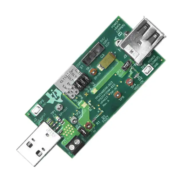
TPS2540EVM-623: Evaluation Module for TPS2540/40A
and TPS2541/41A
This User’s Guide describes the evaluation module (EVM) for the TPS2540/40A and TPS2541/41A.
TPS2540/40A and TPS2541/41A are USB charging port power switch/ controllers for host charging ports
and dedicated charging ports.
1
2
3
4
5
Contents
Description ...................................................................................................................
1.1
Features .............................................................................................................
1.2
Applications .........................................................................................................
1.3
Glossary of Terms .................................................................................................
Schematic ....................................................................................................................
General Configuration and Description ..................................................................................
3.1
Physical Access ....................................................................................................
3.2
Current Limit Setpoint .............................................................................................
3.3
Test Setup ..........................................................................................................
EVM Assembly Drawings and Layout Guidelines ......................................................................
4.1
Layout Guidelines ..................................................................................................
4.2
PCB Drawings ......................................................................................................
Bill of Materials ..............................................................................................................
2
2
2
2
3
4
4
5
5
6
6
6
9
List of Figures
1
TPS2540EVM-623 Schematic............................................................................................. 3
2
Typical TPS2540EVM-623 Test Setup ................................................................................... 5
3
Top Side Placement and Routing ......................................................................................... 6
4
Layer Two Routing .......................................................................................................... 7
5
Layer Three Routing ........................................................................................................ 7
6
Bottom Side Placement and Routing ..................................................................................... 8
List of Tables
1
Connector Functionality .................................................................................................... 4
2
Test Points ................................................................................................................... 4
3
Jumpers ...................................................................................................................... 4
4
TPS2540/40A Mode Truth Table
5
TPS2541/41A Mode Truth Table
6
.........................................................................................
.........................................................................................
TPS2540/40A/41/41A EVM Bill of Materials ............................................................................
SLVU401B – September 2010 – Revised August 2011
Submit Documentation Feedback
TPS2540EVM-623: Evaluation Module for TPS2540/40A and TPS2541/41A
Copyright © 2010–2011, Texas Instruments Incorporated
4
5
9
1
�Description
1
www.ti.com
Description
The TPS2540EVM-623 allows reference circuit evaluation of the TI TPS2540/40A and TPS2541/41A USB
charging port power switch and controller. TPS2540EVM-623 orderable configuration is equipped with
TPS2540RTE but the TPS2540A or TPS2541/41A may also be evaluated by replacing U1 with the
appropriate device.
1.1
Features
•
•
•
•
•
•
•
•
•
•
1.2
Applications
•
•
1.3
USB Ports/Hubs
Notebook PCs
Glossary of Terms
•
•
•
•
2
USB Charging Port Power Switch and Controller
Meets Battery Charging Specification BC1.2 for DCP and CDP
Meets Chinese Telecommunications Industry 2.0 Standard YD/T 1591-2009
Compatible With USB 2.0 and 3.0 Power Switch Requirements
Adjustable Current-limit, 230 mA – 2800 mA typical
Fast Over-current Response – 1.5 μS Typical
73-mΩ High-Side MOSFET
2.6-GHz Bandwidth USB 2.0 Data Switch
OUT Discharge Through CTLx=000 (TPS2540/40A) or DSC (TPS2541/41A)
Longer Detach Detection Time (TPS2540A/41A) Supporting Additional Legacy Devices
Charging Downstream Port (CDP)
– Downstream port complies with the USB 2.0 definition of a host or a hub, and additionally defines a
handshake on DP/DM to identify a BC 1.1 compliant host to a BC 1.1 compliant portable device
– BC 1.1 allows high-speed portable device to draw 900mA and low-speed or full-speed device to
draw 1500mA
– BC 1.2 intention is to allow all devices to draw 1500mA
– BC 1.2 corrects BC 1.1 to ensure USB Host provides 5V at >1500mA
Standard Downstream Port (SDP)
– USB 2.0 defined port currently adopted by most USB ports
– Portable device is allowed to draw 100mA initially and request additional current over USB
communications in 100mA steps up to a maximum of 500mA
– USB Host required to provide 5V at >500mA
– Portable device must not draw >2.5mA when not USB in Suspend due to lack of USB
communication
Dedicated Charging Port as defined in BC 1.1
– BC 1.1 defines a Dedicated Charging Port as a downstream port on a device that outputs power
through a USB connector, but is not capable of enumerating a downstream device.
– Wall adapter must source between 500mA and 1500mA
– Portable Device may attempt to draw 1800mA in order to force the wall adapter into constant
current mode
– BC 1.2 intention is to allow DCP to current limit >1800mA to allow IC power switch device
YD/T 1591-2006, updated 2009
– PROC Telecommunications Standard
– Defines wall-adapter requirements
– Rated current between 500mA – 1500mA w/ defined I-V curve
TPS2540EVM-623: Evaluation Module for TPS2540/40A and TPS2541/41A
SLVU401B – September 2010 – Revised August 2011
Submit Documentation Feedback
Copyright © 2010–2011, Texas Instruments Incorporated
�Schematic
www.ti.com
2
Schematic
+
2
1
2
Figure 1. TPS2540EVM-623 Schematic
spacer
SLVU401B – September 2010 – Revised August 2011
Submit Documentation Feedback
TPS2540EVM-623: Evaluation Module for TPS2540/40A and TPS2541/41A
Copyright © 2010–2011, Texas Instruments Incorporated
3
�General Configuration and Description
www.ti.com
3
General Configuration and Description
3.1
Physical Access
Table 1 lists the TPS2540EVM-623 connector functionality, Table 2 describes the test point availability
and Table 3 describes the jumper functionality.
Table 1. Connector Functionality
Connector
Label
Description
J1
AUX
Auxiliary high current input connector.
J2
USB INPUT
USB input port.
J3A
(UPPER)
Primary charging port (with data).
J3B
(LOWER)
Auxiliary charging port (no data).
D1 (RED)
FAULT
D2 (GREEN)
VOUT-ON
S1
S1
Fault LED
USB Output Powered
Mode switch used in conjunction with Table 4
Table 2. Test Points
(1)
Test Point
Color
Label
TP3
RED
IN
Description
TP4
RED
VOUT
Power bus output.
TP5
SM
TP3
Power bus GND.
TP1
WHT
DP-OUT
Data+ out
TP2
WHT
DM-OUT
Data- out
Power bus input.
TP6
SM
TP5
TP7 (1)
ORG
DP-IN
Power bus GND
Data+ in
TP8 (1)
ORG
DM-IN
Data- in
TP7 and TP8 are isolated from U1 DP_IN (U1-11) and DM_IN (U1-10) respectively with 1MΩ resistors to minimize degradation
of high speed signal quality. Static voltage measurements of U1 DP_IN or DM_IN through TP7 and TP8 will be affected by the
loading of the test instrument and 1MΩ resistors.
Table 3. Jumpers
Jumper
Label
JP1
VIN
Description
JP2
VOUT
Power bus output. Install shunt to allow charger source to power downstream devices.
JP3
CTL3
CTL3. See MODE truth table
JP4
CTL2
CTL2. See MODE truth table
JP5
CTL1
CTL1. See MODE truth table
JP6
EN
TPS2540/40A/41/41A Enable select. Install shunt to disable TPS2540/40A/41/41A (also discharges the output capacitor for
TPS2541/41A).
JP7
ILIM
ILIM select. Install shunt to select ILIM0 (2.43A typical ILIM). Remove shunt to select ILIM1 (1.21A typical ILIM).
Power bus input. Install shunt to allow charger source to power TPS2540/1 and downstream circuitry.
The CTL pins configure the device mode. Setting S1 to the CDP position (open) is equivalent to setting
the CTL pins to the state in the last row of Table 4. Setting S1 to the DIS/SDP/DCP position allows the
remaining rows to be configured.
Table 4. TPS2540/40A Mode Truth Table
4
CTL1 (JP5)
CTL2 (JP4)
CTL3 (JP3)
0
0
0
Mode
OUT discharge, power switch OFF
0
X
1
Dedicated Charging Port, Auto-detect
X
1
0
Standard Downstream Port, USB 2.0 Mode
1
0
0
Dedicated Charging Port, BC Specification 1.1 only
TPS2540EVM-623: Evaluation Module for TPS2540/40A and TPS2541/41A
SLVU401B – September 2010 – Revised August 2011
Submit Documentation Feedback
Copyright © 2010–2011, Texas Instruments Incorporated
�General Configuration and Description
www.ti.com
Table 4. TPS2540/40A Mode Truth Table (continued)
CTL1 (JP5)
CTL2 (JP4)
CTL3 (JP3)
1
0
1
Mode
Dedicated Charging Port, divider mode only
1
1
1
Charging Downstream Port, BC Specification 1.1
The CTL pins configure the device mode. Setting S1 to the CDP position (open) is equivalent to setting
the CTL pins to the state in the last row of Table 5. Setting S1 to the DIS/SDP/DCP position allows the
remaining rows to be configured.
Table 5. TPS2541/41A Mode Truth Table
3.2
CTL1 (JP5)
CTL2 (JP4)
CTL3 (JP3)
Mode
0
0
X
Dedicated Charging Port, Auto-detect
0
1
X
Dedicated Charging Port, BC 1.1 Specification Only
1
0
X
Dedicated Charging Port, divider mode only
1
1
0
Standard Charging Port, USB 2.0 Mode
1
1
1
Charging Downstream Port, BC Specification 1.1
Current Limit Setpoint
R2 and R3 configure the current limit setpoint for ILIM0 and ILIM1 respectively (see JP7 in Table 3). ILIM0
or ILIM1 setpoint can be adjusted using the following example by substituting R2 or R3 for RILIMx. In this
example IOS = 2A.
The example below is an approximation only and does not take into account the resistor tolerance or the
variation of ILIM. For exact variation of ILIM, see the TPS2540/40A/TPS2541/41/A data sheet, SLVSAG2.
IOS = 48000 / RILIMx = 2 A
RILIMx = 48000 / IOS = 48000 / 2 = 24000 Ω
Choose RILIMx = 23.7 kΩ
IOS = 48000 / 23700 = 2.03 A
3.3
Test Setup
Figure 2 shows a typical test setup for TPS2540EVM-623. Connect J2 to the PC either directly (insert J2
into available/accessible PC USB port) or using any Type A Male to Type A Female USB v2.0 extension
cable. USB power and data are available at J3A and USB power only is available at J3B.
PC (USB charging source)
S1
JPR
J2
J3A
Load1
J3B
Load2
TPS2540/1EVM
J1
D1
D2
Figure 2. Typical TPS2540EVM-623 Test Setup
SLVU401B – September 2010 – Revised August 2011
Submit Documentation Feedback
TPS2540EVM-623: Evaluation Module for TPS2540/40A and TPS2541/41A
Copyright © 2010–2011, Texas Instruments Incorporated
5
�EVM Assembly Drawings and Layout Guidelines
4
EVM Assembly Drawings and Layout Guidelines
4.1
Layout Guidelines
•
•
•
•
4.2
www.ti.com
TPS2540/40A/41/41A placement: Place the TPS2540/41 near the USB output connector and 150µF
OUT pin filter capacitor. Connect the exposed pad to the GND pin and the system ground plane using
an array of vias.
IN pin bypass capacitance: Place the 0.1µF bypass capacitor near the IN pin and make the connection
using a low inductance trace.
DP-OUT/DM-OUT, DP-IN/DM-IN traces: Route these traces as controlled impedance differential pairs
per the USB-2.0 specification. Minimize the use of vias in the high speed data lines. Figure 6 provides
a good signal routing example for the high speed data traces. In this example, the data pairs are
routed as edge-coupled microstrips with nominal differential impedance of 90 ohms. The reference
plane is tied to GND and is shown in Figure 5. Ensure that the reference plane is void of cuts or splits
above the differential pairs to prevent impedance discontinuities.
ILIM0 and ILIM1 Pin Connections: Current-limit, set-point accuracy can be compromised by stray
current leakage from a higher voltage source to the ILIM0 or ILIM1 pins. Ensure that there is adequate
spacing between IN pin copper/trace and ILIM0 pin trace to prevent contaminant buildup during the
PCB assembly process. If a low-current-limit set point is required (RILIMx > 200 kΩ), use ILIM1 for this
case as it is further away from the IN pin.
PCB Drawings
The following figures show component placement and layout of the EVM.
Figure 3. Top Side Placement and Routing
6
TPS2540EVM-623: Evaluation Module for TPS2540/40A and TPS2541/41A
SLVU401B – September 2010 – Revised August 2011
Submit Documentation Feedback
Copyright © 2010–2011, Texas Instruments Incorporated
�EVM Assembly Drawings and Layout Guidelines
www.ti.com
Figure 4. Layer Two Routing
Figure 5. Layer Three Routing
SLVU401B – September 2010 – Revised August 2011
Submit Documentation Feedback
TPS2540EVM-623: Evaluation Module for TPS2540/40A and TPS2541/41A
Copyright © 2010–2011, Texas Instruments Incorporated
7
�EVM Assembly Drawings and Layout Guidelines
www.ti.com
Figure 6. Bottom Side Placement and Routing
8
TPS2540EVM-623: Evaluation Module for TPS2540/40A and TPS2541/41A
SLVU401B – September 2010 – Revised August 2011
Submit Documentation Feedback
Copyright © 2010–2011, Texas Instruments Incorporated
�Bill of Materials
www.ti.com
5
Bill of Materials
Table 6. TPS2540/40A/41/41A EVM Bill of Materials
Count
REFDES
Value
Description
Size
Part Number
Supplier
1
C1
10 µF
Capacitor, Ceramic, 10V, X5R, 10%
0805
Std
Std
2
C2, C4
0.1 µF
Capacitor, Ceramic, 50V, X7R, 10%
0603
Std
Std
1
C3
150 µF
Capacitor, Tant, Low ESR, 10V, ±10%
7343 (D)
TPSD157K010R0100
AVX
1
D1
LN1271R
Diode, LED, Red, 10-mA, 0.4-mcd
0.114 X 0.049 inch
LN1271RTR
Panasonic
1
D2
LN1371G
Diode, LED, Green, 10-mA, 2.6-mcd
0.114 X 0.049 inch
LN1371GTR
Panasonic
1
J1
ED555/2DS
Terminal Block, 2-pin, 6-A, 3.5mm
0.27 x 0.25 inch
ED555/2DS
OST
1
J2
48037-1000
Connector, USB A, Plug RA, 4pin
0.500 X 0.740 inch
48037-1000
Molex
1
J3
896-43-008-90-000000
Connector, Dual USB Downstream (Type A)
0.52 x 0.67 inch
896-43-008-90-000000
Mill-Max
7
JP1, JP2, JP3, JP4,
JP5, JP6, JP7
PEC02SAAN
Header, Male 2-pin, 100mil spacing,
0.100 inch x 2
PEC02SAAN
Sullins
1
L1
370-Ohm
Inductor, Coupled
0.050 x 0.080 inch
0805USB-372ML
Coilcraft
2
R1, R4
2k
Resistor, Chip, 1/16W, 1%
0603
Std
Std
1
R2
20k
Resistor, Chip, 1/16W, 1%
0603
Std
Std
1
R3
40.2k
Resistor, Chip, 1/16W, 1%
0603
Std
Std
4
R5, R6, R7, R8
1M
Resistor, Chip, 1/16W, 1%
0402
Std
Std
5
R9, R10, R11, R12, R13 100k
Resistor, Chip, 1/16W, 1%
0402
Std
Std
1
S1
EG1218
Switch, 1P2T, Slide, PC-mount, 200-mA
0.46 x 0.16
EG1218
E_Switch
2
TP1, TP2
5012
Test Point, White, Thru Hole
0.125 x 0.125 inch
5012
Keystone
2
TP3, TP4
5010
Test Point, Red, Thru Hole
0.125 x 0.125 inch
5010
Keystone
2
TP5, TP6
5016
Test Point, SM, 0.150 x 0.090
0.185 x 0.135 inch
5016
Keystone
2
TP7, TP8
5013
Test Point, Orange, Thru Hole
0.125 x 0.125 inch
5013
Keystone
1
U1
TPS2540
IC, USB Charging Port Power Switch and
Controller
QFN-16
TPS2540RTE
TI
1
U2
TPD2E001DZDR
IC, Low-Capacitance 2-Chan ±15-kV
ESD-Protection Array
SOP
TPD2E001DZDR
TI
5
—
Shunt, Black
100-mil
STC02SYAN
Sullins
1
—
PCB, 2.5 In x 1.20 In x 0.062 In
HPA623
Any
SLVU401B – September 2010 – Revised August 2011
Submit Documentation Feedback
TPS2540EVM-623: Evaluation Module for TPS2540/40A and TPS2541/41A
Copyright © 2010–2011, Texas Instruments Incorporated
9
�Evaluation Board/Kit Important Notice
Texas Instruments (TI) provides the enclosed product(s) under the following conditions:
This evaluation board/kit is intended for use for ENGINEERING DEVELOPMENT, DEMONSTRATION, OR EVALUATION
PURPOSES ONLY and is not considered by TI to be a finished end-product fit for general consumer use. Persons handling the
product(s) must have electronics training and observe good engineering practice standards. As such, the goods being provided are
not intended to be complete in terms of required design-, marketing-, and/or manufacturing-related protective considerations,
including product safety and environmental measures typically found in end products that incorporate such semiconductor
components or circuit boards. This evaluation board/kit does not fall within the scope of the European Union directives regarding
electromagnetic compatibility, restricted substances (RoHS), recycling (WEEE), FCC, CE or UL, and therefore may not meet the
technical requirements of these directives or other related directives.
Should this evaluation board/kit not meet the specifications indicated in the User’s Guide, the board/kit may be returned within 30
days from the date of delivery for a full refund. THE FOREGOING WARRANTY IS THE EXCLUSIVE WARRANTY MADE BY
SELLER TO BUYER AND IS IN LIEU OF ALL OTHER WARRANTIES, EXPRESSED, IMPLIED, OR STATUTORY, INCLUDING
ANY WARRANTY OF MERCHANTABILITY OR FITNESS FOR ANY PARTICULAR PURPOSE.
The user assumes all responsibility and liability for proper and safe handling of the goods. Further, the user indemnifies TI from all
claims arising from the handling or use of the goods. Due to the open construction of the product, it is the user’s responsibility to
take any and all appropriate precautions with regard to electrostatic discharge.
EXCEPT TO THE EXTENT OF THE INDEMNITY SET FORTH ABOVE, NEITHER PARTY SHALL BE LIABLE TO THE OTHER
FOR ANY INDIRECT, SPECIAL, INCIDENTAL, OR CONSEQUENTIAL DAMAGES.
TI currently deals with a variety of customers for products, and therefore our arrangement with the user is not exclusive.
TI assumes no liability for applications assistance, customer product design, software performance, or infringement of
patents or services described herein.
Please read the User’s Guide and, specifically, the Warnings and Restrictions notice in the User’s Guide prior to handling the
product. This notice contains important safety information about temperatures and voltages. For additional information on TI’s
environmental and/or safety programs, please contact the TI application engineer or visit www.ti.com/esh.
No license is granted under any patent right or other intellectual property right of TI covering or relating to any machine, process, or
combination in which such TI products or services might be or are used.
FCC Warning
This evaluation board/kit is intended for use for ENGINEERING DEVELOPMENT, DEMONSTRATION, OR EVALUATION
PURPOSES ONLY and is not considered by TI to be a finished end-product fit for general consumer use. It generates, uses, and
can radiate radio frequency energy and has not been tested for compliance with the limits of computing devices pursuant to part 15
of FCC rules, which are designed to provide reasonable protection against radio frequency interference. Operation of this
equipment in other environments may cause interference with radio communications, in which case the user at his own expense
will be required to take whatever measures may be required to correct this interference.
EVM Warnings and Restrictions
It is important to operate this EVM within the input voltage range of 0 V to 5.5 V and the output voltage range of 0 V to 5.5 V .
Exceeding the specified input range may cause unexpected operation and/or irreversible damage to the EVM. If there are
questions concerning the input range, please contact a TI field representative prior to connecting the input power.
Applying loads outside of the specified output range may result in unintended operation and/or possible permanent damage to the
EVM. Please consult the EVM User's Guide prior to connecting any load to the EVM output. If there is uncertainty as to the load
specification, please contact a TI field representative.
During normal operation, some circuit components may have case temperatures greater than 85°C. The EVM is designed to
operate properly with certain components above 85°C as long as the input and output ranges are maintained. These components
include but are not limited to linear regulators, switching transistors, pass transistors, and current sense resistors. These types of
devices can be identified using the EVM schematic located in the EVM User's Guide. When placing measurement probes near
these devices during operation, please be aware that these devices may be very warm to the touch.
Mailing Address: Texas Instruments, Post Office Box 655303, Dallas, Texas 75265
Copyright © 2011, Texas Instruments Incorporated
�IMPORTANT NOTICE
Texas Instruments Incorporated and its subsidiaries (TI) reserve the right to make corrections, modifications, enhancements, improvements,
and other changes to its products and services at any time and to discontinue any product or service without notice. Customers should
obtain the latest relevant information before placing orders and should verify that such information is current and complete. All products are
sold subject to TI’s terms and conditions of sale supplied at the time of order acknowledgment.
TI warrants performance of its hardware products to the specifications applicable at the time of sale in accordance with TI’s standard
warranty. Testing and other quality control techniques are used to the extent TI deems necessary to support this warranty. Except where
mandated by government requirements, testing of all parameters of each product is not necessarily performed.
TI assumes no liability for applications assistance or customer product design. Customers are responsible for their products and
applications using TI components. To minimize the risks associated with customer products and applications, customers should provide
adequate design and operating safeguards.
TI does not warrant or represent that any license, either express or implied, is granted under any TI patent right, copyright, mask work right,
or other TI intellectual property right relating to any combination, machine, or process in which TI products or services are used. Information
published by TI regarding third-party products or services does not constitute a license from TI to use such products or services or a
warranty or endorsement thereof. Use of such information may require a license from a third party under the patents or other intellectual
property of the third party, or a license from TI under the patents or other intellectual property of TI.
Reproduction of TI information in TI data books or data sheets is permissible only if reproduction is without alteration and is accompanied
by all associated warranties, conditions, limitations, and notices. Reproduction of this information with alteration is an unfair and deceptive
business practice. TI is not responsible or liable for such altered documentation. Information of third parties may be subject to additional
restrictions.
Resale of TI products or services with statements different from or beyond the parameters stated by TI for that product or service voids all
express and any implied warranties for the associated TI product or service and is an unfair and deceptive business practice. TI is not
responsible or liable for any such statements.
TI products are not authorized for use in safety-critical applications (such as life support) where a failure of the TI product would reasonably
be expected to cause severe personal injury or death, unless officers of the parties have executed an agreement specifically governing
such use. Buyers represent that they have all necessary expertise in the safety and regulatory ramifications of their applications, and
acknowledge and agree that they are solely responsible for all legal, regulatory and safety-related requirements concerning their products
and any use of TI products in such safety-critical applications, notwithstanding any applications-related information or support that may be
provided by TI. Further, Buyers must fully indemnify TI and its representatives against any damages arising out of the use of TI products in
such safety-critical applications.
TI products are neither designed nor intended for use in military/aerospace applications or environments unless the TI products are
specifically designated by TI as military-grade or "enhanced plastic." Only products designated by TI as military-grade meet military
specifications. Buyers acknowledge and agree that any such use of TI products which TI has not designated as military-grade is solely at
the Buyer's risk, and that they are solely responsible for compliance with all legal and regulatory requirements in connection with such use.
TI products are neither designed nor intended for use in automotive applications or environments unless the specific TI products are
designated by TI as compliant with ISO/TS 16949 requirements. Buyers acknowledge and agree that, if they use any non-designated
products in automotive applications, TI will not be responsible for any failure to meet such requirements.
Following are URLs where you can obtain information on other Texas Instruments products and application solutions:
Products
Applications
Audio
www.ti.com/audio
Communications and Telecom www.ti.com/communications
Amplifiers
amplifier.ti.com
Computers and Peripherals
www.ti.com/computers
Data Converters
dataconverter.ti.com
Consumer Electronics
www.ti.com/consumer-apps
DLP® Products
www.dlp.com
Energy and Lighting
www.ti.com/energy
DSP
dsp.ti.com
Industrial
www.ti.com/industrial
Clocks and Timers
www.ti.com/clocks
Medical
www.ti.com/medical
Interface
interface.ti.com
Security
www.ti.com/security
Logic
logic.ti.com
Space, Avionics and Defense
www.ti.com/space-avionics-defense
Power Mgmt
power.ti.com
Transportation and
Automotive
www.ti.com/automotive
Microcontrollers
microcontroller.ti.com
Video and Imaging
www.ti.com/video
RFID
www.ti-rfid.com
Wireless
www.ti.com/wireless-apps
RF/IF and ZigBee® Solutions
www.ti.com/lprf
TI E2E Community Home Page
e2e.ti.com
Mailing Address: Texas Instruments, Post Office Box 655303, Dallas, Texas 75265
Copyright © 2011, Texas Instruments Incorporated
�