Sample &
Buy
Product
Folder
Support &
Community
Tools &
Software
Technical
Documents
TPS2556, TPS2557
SLVS931B – NOVEMBER 2009 – REVISED DECEMBER 2016
TPS255x Precision Adjustable Current-Limited Power-Distribution Switches
1 Features
3 Description
•
•
•
•
•
•
•
•
•
•
The TPS255x power-distribution switch is intended
for applications where precision current limiting is
required or heavy capacitive loads and short circuits
are
encountered.
These
devices
offer
a
programmable current-limit threshold between
500 mA and 5 A (typical) through an external resistor.
The power-switch rise and fall times are controlled to
minimize current surges during turnon and turnoff.
1
Meets USB Current-Limiting Requirements
Adjustable Current Limit, 500 mA to 5 A (Typical)
±6.5% Current-Limit Accuracy at 4.5 A
Fast Overcurrent Response: 3.5-µs (Typical)
22-mΩ High-Side MOSFET
Operating Voltage: 2.5 V to 6.5 V
2-µA Maximum Standby Supply Current
Built-in Soft Start
15-kV and 8-kV System-Level ESD Capable
UL Listed: File No. E169910 and CB IEC60950-1am2 ed2.0
TPS255x devices limit the output current to a safe
level by switching into a constant-current mode when
the output load exceeds the current-limit threshold.
The FAULT logic output asserts low during
overcurrent and overtemperature conditions.
Device Information(1)
2 Applications
•
•
•
•
PART NUMBER
USB Ports and Hubs
Digital TVs
Set-Top Boxes
VOIP Phones
TPS2556, TPS2557
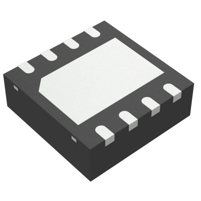
PACKAGE
VSON (8)
BODY SIZE (NOM)
3.00 mm × 3.00 mm
(1) For all available packages, see the orderable addendum at
the end of the data sheet.
Typical Application as USB Power Switch
2.5V – 6.5V
R FAULT
100 kΩ
0.1 uF
IN
IN
VOUT
OUT
OUT
R ILIM
Fault Signal
Control Signal
FAULT
EN
CLOAD
ILIM
GND
Power Pad
Copyright © 2016, Texas Instruments Incorporated
1
An IMPORTANT NOTICE at the end of this data sheet addresses availability, warranty, changes, use in safety-critical applications,
intellectual property matters and other important disclaimers. PRODUCTION DATA.
�TPS2556, TPS2557
SLVS931B – NOVEMBER 2009 – REVISED DECEMBER 2016
www.ti.com
Table of Contents
1
2
3
4
5
6
7
8
9
Features ..................................................................
Applications ...........................................................
Description .............................................................
Revision History.....................................................
Device Comparison Table.....................................
Pin Configuration and Functions .........................
Specifications.........................................................
1
1
1
2
3
3
4
7.1
7.2
7.3
7.4
7.5
7.6
7.7
4
4
4
5
5
6
7
Absolute Maximum Ratings ......................................
ESD Ratings..............................................................
Recommended Operating Conditions.......................
Thermal Information ..................................................
Electrical Characteristics...........................................
Switching Characteristics ..........................................
Typical Characteristics ..............................................
Parameter Measurement Information ................ 10
Detailed Description ............................................ 11
9.1 Overview ................................................................. 11
9.2 Functional Block Diagram ....................................... 11
9.3 Feature Description................................................. 11
9.4 Device Functional Modes........................................ 12
10 Application and Implementation........................ 13
10.1 Application Information.......................................... 13
10.2 Typical Applications .............................................. 13
11 Power Supply Recommendations ..................... 18
12 Layout................................................................... 19
12.1 Layout Guidelines ................................................. 19
12.2 Layout Example .................................................... 19
12.3 Thermal Considerations ........................................ 20
13 Device and Documentation Support ................. 21
13.1
13.2
13.3
13.4
13.5
13.6
Related Links ........................................................
Receiving Notification of Documentation Updates
Community Resources..........................................
Trademarks ...........................................................
Electrostatic Discharge Caution ............................
Glossary ................................................................
21
21
21
21
21
21
14 Mechanical, Packaging, and Orderable
Information ........................................................... 21
4 Revision History
NOTE: Page numbers for previous revisions may differ from page numbers in the current version.
Changes from Revision A (Feburary 2012) to Revision B
Page
•
Added Device Information table, Device Comparison Table, Pin Configuration and Functions section, Specifications
section, ESD Ratings table, Application and Implementation section, Power Supply Recommendations section,
Layout section, Device and Documentation Support section, and Mechanical, Packaging, and Orderable Information
section .................................................................................................................................................................................... 1
•
Deleted Ordering Information table; see Package Option Addendum at the end of the data sheet ...................................... 1
•
Added Thermal Information table ........................................................................................................................................... 5
•
Changed RθJC(top) value in Thermal Information table From: 10.7°C/W To: 54.5°C/W ........................................................... 5
•
Changed Figure 11 title From: Current Limit Threshold Vs RILM To: Switch Current vs Drain-Source Voltage Across
Switch ..................................................................................................................................................................................... 7
•
Changed Figure 12 title From: Current Limit Threshold Vs RILM To: Switch Current vs Drain-Source Voltage Across
Switch ..................................................................................................................................................................................... 7
Changes from Original (November 2009) to Revision A
Page
•
Changed VEN to VEN in Recommended Operating Conditions table ...................................................................................... 4
•
Changed VEN to VEN in Recommended Operating Conditions table ...................................................................................... 4
2
Submit Documentation Feedback
Copyright © 2009–2016, Texas Instruments Incorporated
Product Folder Links: TPS2556 TPS2557
�TPS2556, TPS2557
www.ti.com
SLVS931B – NOVEMBER 2009 – REVISED DECEMBER 2016
5 Device Comparison Table
33 mΩ, SINGLE
80 mΩ, SINGLE
80 mΩ, DUAL
80 mΩ, DUAL
80 mΩ, TRIPLE
80 mΩ, QUAD
80 mΩ, QUAD
TPS201xA
0.2 A–2 A
TPS2014
600 mA
TPS202x
0.2 A–2 A
TPS2015
1A
TPS2042B
500 mA
TPS2080
500 mA
TPS203x
0.2 A–2 A
TPS2041B
500 mA
TPS2052B
500 mA
TPS2081
500 mA
TPS2043B
500 mA
TPS2051B
500 mA
TPS2046B
250 mA
TPS2082
500 mA
TPS2053B
500 mA
TPS2044B
500 mA
TPS2085
500 mA
TPS2045A
250 mA
TPS2056
250 mA
TPS2090
250 mA
TPS2047B
250 mA
TPS2054B
500 mA
TPS2086
500 mA
TPS2049
100 mA
TPS2062
1A
TPS2091
250 mA
TPS2057A
250 mA
TPS2048A
250 mA
TPS2087
500 mA
TPS2055A
250 mA
TPS2066
1A
TPS2092
250 mA
TPS2063
1A
TPS2058
250 mA
TPS2095
250 mA
TPS2061
1A
TPS2060
1.5 A
TPS2067
1A
TPS2096
250 mA
TPS2065
1A
TPS2064
1.5 A
TPS2097
250 mA
TPS2068
1.5 A
TPS2069
1.5 A
6 Pin Configuration and Functions
DRB Package
8-Pin VSON
Top View
GND
1
IN
2
8
FAULT
7
OUT
PowerPAD
IN
3
6
OUT
EN
4
5
ILIM
Not to scale
TPS2556: EN pin is active low.
TPS2557: EN pin is active high.
Pin Functions
PIN
NAME
I/O
DESCRIPTION
TPS2556
TPS2557
EN
4
—
I
Enable input: Logic low turns on power switch. Applicable to the TPS2556.
EN
—
4
I
Enable input: Logic high turns on power switch. Applicable to the TPS2557.
FAULT
8
8
O
Active-low open-drain output: Asserted during overcurrent or overtemperature
conditions.
GND
1
1
—
Ground connection: Connect externally to PowerPAD.
ILIM
5
5
O
External resistor used to set current-limit threshold. TI recommends
20 kΩ ≤ RILIM ≤ 187 kΩ.
IN
2, 3
2, 3
I
Input voltage: Connect a 0.1-µF or greater ceramic capacitor from IN to GND as
close to the IC as possible.
OUT
6, 7
6, 7
O
Power-switch output.
PowerPAD
PowerPAD
—
Internally connected to GND. Used to heat-sink the part to the circuit board
traces. Connect PowerPAD to GND pin externally.
PowerPAD™
Copyright © 2009–2016, Texas Instruments Incorporated
Product Folder Links: TPS2556 TPS2557
Submit Documentation Feedback
3
�TPS2556, TPS2557
SLVS931B – NOVEMBER 2009 – REVISED DECEMBER 2016
www.ti.com
7 Specifications
7.1 Absolute Maximum Ratings
over operating free-air temperature range (unless otherwise noted) (1) (2)
MIN
MAX
UNIT
–0.3
7
V
Voltage from IN to OUT
–7
7
V
Continuous output current
Internally limited
Voltage
IN, OUT, EN or EN, ILIM, and FAULT pins
Continuous FAULT sink current
25
ILIM source current
mA
Internally limited
Continuous total power dissipation
See Thermal Information
Maximum junction temperature
–40
OTSD2
°C
Storage temperature, Tstg
-65
150
°C
(1)
(2)
Stresses beyond those listed under Absolute Maximum Ratings may cause permanent damage to the device. These are stress ratings
only, which do not imply functional operation of the device at these or any other conditions beyond those indicated under Recommended
Operating Conditions. Exposure to absolute-maximum-rated conditions for extended periods may affect device reliability.
Voltages are referenced to GND unless otherwise noted.
7.2 ESD Ratings
VALUE
Human-body model (HBM), per ANSI/ESDA/JEDEC JS-001 (1)
V(ESD)
(1)
(2)
(3)
Electrostatic discharge
UNIT
±2000
Charged-device model (CDM), per JEDEC specification JESD22-C101 (2)
±500
IEC 61000-4-2 contact discharge (3)
±8000
IEC 61000-4-2 air discharge (3)
±15000
V
JEDEC document JEP155 states that 500-V HBM allows safe manufacturing with a standard ESD control process.
JEDEC document JEP157 states that 250-V CDM allows safe manufacturing with a standard ESD control process.
Surges per EN61000-4-2, 1999 applied between USB and output ground of the TPS2556EVM (HPA423) evaluation module (see Using
the TPS2556EVM-423 and TPS2557EVM-423). These were the test levels, not the failure threshold.
7.3 Recommended Operating Conditions
VIN
VEN
VEN
MIN
MAX
2.5
6.5
TPS2556
0
6.5
TPS2557
0
6.5
Input voltage, IN
Enable voltage
VIH
High-level input voltage on Enable pin
VIL
Low-level input voltage on Enable pin
IOUT
Continuous output current (OUT pin)
1.1
0.66
0
Continuous FAULT sink current
RILIM
Recommended resistor limit
TJ
Operating virtual junction temperature
4
Submit Documentation Feedback
UNIT
V
V
V
5
A
0
10
mA
20
187
kΩ
–40
125
°C
Copyright © 2009–2016, Texas Instruments Incorporated
Product Folder Links: TPS2556 TPS2557
�TPS2556, TPS2557
www.ti.com
SLVS931B – NOVEMBER 2009 – REVISED DECEMBER 2016
7.4 Thermal Information
TPS255x
THERMAL METRIC (1)
DRB (VSON)
UNIT
8 PINS
RθJA
Junction-to-ambient thermal resistance
41.5
°C/W
RθJC(top)
Junction-to-case (top) thermal resistance
54.5
°C/W
RθJB
Junction-to-board thermal resistance
16.4
°C/W
ψJT
Junction-to-top characterization parameter
0.7
°C/W
ψJB
Junction-to-board characterization parameter
16.6
°C/W
RθJC(bot)
Junction-to-case (bottom) thermal resistance
3.6
°C/W
(1)
For more information about traditional and new thermal metrics, see the Semiconductor and IC Package Thermal Metrics application
report.
7.5 Electrical Characteristics
over recommended operating conditions, VEN = 0 V or VEN = VIN (unless otherwise noted) (1)
PARAMETER
TEST CONDITIONS
MIN
TYP
MAX
22
25
UNIT
POWER SWITCH
rDS(ON)
TJ = 25°C
Static drain-source on-state resistance
–40°C ≤TJ ≤ 125°C
35
Enable pin turn on and off threshold
0.66
Enable input hysteresis (2)
IEN
Input current
Current-limit threshold (Maximum DC output
current IOUT delivered to load) and shortcircuit current, OUT connected to GND
IOS
IIN_OFF
1.1
55
Supply current, low-level output
V
mV
VEN = 0 V or 6.5 V, VEN = 0 V or 6.5 V
–0.5
RILIM = 24.9 kΩ
4130
4450
4695
RILIM = 61.9 kΩ
1590
1785
1960
RILIM = 100 kΩ
935
1100
1260
VIN = 6.5 V, No load on OUT, VEN = 6.5 V or VEN = 0 V
mΩ
0.5
µA
mA
0.1
2
µA
RILIM = 24.9 kΩ
95
120
µA
RILIM = 100 kΩ
85
110
µA
IIN_ON
Supply current, high-level output
VIN = 6.5 V, No load on OUT
IREV
Reverse leakage current
VOUT = 6.5 V, VIN = 0 V, TJ = 25 °C
0.01
1
µA
UVLO
Low-level input voltage (IN pin)
VIN rising
2.35
2.45
V
UVLO hysteresis (IN pin)
(2)
35
mV
FAULT FLAG
VOL
Output low voltage (FAULT pin)
IFAULT = 1 mA
Off-state leakage
VFAULT = 6.5 V
FAULT deglitch
FAULT assertion or deassertion due to overcurrent
condition
6
9
180
mV
1
µA
13
ms
THERMAL SHUTDOWN
OTSD2
Thermal shutdown threshold
155
OTSD
Thermal shutdown threshold in current-limit
135
Hysteresis (2)
(1)
(2)
°C
°C
20
°C
Pulse-testing techniques maintain junction temperature close to ambient temperature; thermal effects must be considered separately.
These parameters are provided for reference only, and do no constitute part of TI's published specifications for purposes of TI's product
warranty.
Copyright © 2009–2016, Texas Instruments Incorporated
Product Folder Links: TPS2556 TPS2557
Submit Documentation Feedback
5
�TPS2556, TPS2557
SLVS931B – NOVEMBER 2009 – REVISED DECEMBER 2016
www.ti.com
7.6 Switching Characteristics
over operating free-air temperature range (unless otherwise noted)
PARAMETER
TEST CONDITIONS
MIN
TYP
MAX
UNIT
tR
Rise time, output
CL = 1 µF, RL= 100 Ω, (see
Figure 15)
VIN = 6.5 V
2
3
4
VIN = 2.5 V
1
2
3
tF
Fall time, output
CL = 1 µF, RL= 100 Ω, (see
Figure 15)
VIN = 6.5 V
0.6
0.8
1
VIN = 2.5 V
0.4
0.6
0.8
tON
Turnon time
CL = 1 µF, RL= 100 Ω, (see Figure 15)
9
ms
tOFF
Turnoff time
CL = 1 µF, RL= 100 Ω, (see Figure 15)
6
ms
tIOS
Response time to short circuit (1)
VIN = 5 V (see Figure 16)
(1)
6
3.5
ms
ms
µs
These parameters are provided for reference only, and do no constitute part of TI's published specifications for purposes of TI's product
warranty.
Submit Documentation Feedback
Copyright © 2009–2016, Texas Instruments Incorporated
Product Folder Links: TPS2556 TPS2557
�TPS2556, TPS2557
www.ti.com
SLVS931B – NOVEMBER 2009 – REVISED DECEMBER 2016
7.7 Typical Characteristics
VOUT
2 V/div
VOUT
2 V/div
VEN_bar
5 V/div
VEN_bar
5 V/div
IIN
2 A/div
IIN
2 A/div
t - Time - 2 ms/div
t - Time - 2 ms/div
Figure 1. Turnon Delay and Rise Time
Figure 2. Turnoff Delay and Fall Time
VEN_bar
5 V/div
VOUT
2 V/div
FAULT_bar
FAULT_bar
5 V/div
5 V/div
IIN
2 A/div
IIN
5 A/div
t - Time - 2 ms/div
t - Time - 5 ms/div
Figure 3. Device Enabled into Short-Circuit
Figure 4. Full-Load to Short-Circuit Transient Response
2.335
2.33
UVLO - Undervoltage Lockout - V
VOUT
2 V/div
FAULT_bar
5 V/div
IIN
5 A/div
2.325
UVLO Rising
2.32
2.315
2.31
2.305
UVLO Falling
2.3
2.295
2.29
-50
t - Time - 5 ms/div
Figure 5. Short-Circuit to Full-Load Recovery Response
Copyright © 2009–2016, Texas Instruments Incorporated
Product Folder Links: TPS2556 TPS2557
0
50
TJ - Junction Temperature - °C
100
150
Figure 6. Undervoltage Lockout
Submit Documentation Feedback
7
�TPS2556, TPS2557
SLVS931B – NOVEMBER 2009 – REVISED DECEMBER 2016
www.ti.com
Typical Characteristics (continued)
120
700
VIN = 6.5 V
IIN - Supply Current, Output Enabled - mA
IIN - Supply Current, Output Disabled - nA
VIN = 5 V
600
500
400
VIN = 6.5 V
300
200
VIN = 2.5 V
100
0
-100
-50
0
50
TJ - Junction Temperature - °C
100
100
80
VIN = 2.5 V
40
RILIM = 24.9 kΩ
20
0
-50
150
0
Figure 7. Supply Current, Output Disabled
50
TJ - Junction Temperature - °C
100
150
Figure 8. Supply Current, Output Enabled
35
rDS(on) - Static Drain-Source On-State Resistance - mW
120
RILIM = 24.9kΩ
IIN Supply Current vs. VIN Enabled - μA
VIN = 3.3 V
60
110
TJ = 125°C
100
90
80
TJ = -40°C
TJ = 25°C
70
3
4
5
Input Voltage - V
6
25
20
15
10
5
0
-50
60
2
30
7
0
50
TJ - Junction Temperature - °C
100
150
Figure 10. MOSFET rDS(ON) vs Junction Temperature
Figure 9. Supply Current, Output Enabled
1.2
2
IDS - Static Drain-Source Current - A
IDS - Static Drain-Source Current - A
1.8
1.0
TA = -40°C
0.8
TA = 25°C
TA = 125°C
0.6
0.4
RILIM = 100 kW
1.6
1.4
TA = -40°C
1.2
TA = 25°C
1.0
TA = 125°C
0.8
0.6
RILIM = 61.9 kW
0.4
0.2
0.2
0
0
0
50
100
VIN - VOUT - mV/div
150
Figure 11. Switch Current vs Drain-Source Voltage
Across Switch
8
Submit Documentation Feedback
200
0
20
40
60
80
100
VIN - VOUT - mV/div
120
140
160
Figure 12. Switch Current vs Drain-Source Voltage
Across Switch
Copyright © 2009–2016, Texas Instruments Incorporated
Product Folder Links: TPS2556 TPS2557
�TPS2556, TPS2557
www.ti.com
SLVS931B – NOVEMBER 2009 – REVISED DECEMBER 2016
Typical Characteristics (continued)
5.0
4.5
IDS - Static Drain-Source Current - A
4.0
TJ = -40°C
3.5
3.0
TJ = 25°C
2.5
2.0
1.5
TJ = 125°C
1.0
RILIM = 24.9kΩ
0.5
0
0
20
40
60
100
80
VIN-VOUT - mV
120
140
160
Figure 13. Switch Current vs Drain-Source Voltage Across Switch
Copyright © 2009–2016, Texas Instruments Incorporated
Product Folder Links: TPS2556 TPS2557
Submit Documentation Feedback
9
�TPS2556, TPS2557
SLVS931B – NOVEMBER 2009 – REVISED DECEMBER 2016
www.ti.com
8 Parameter Measurement Information
TPS2556
VIN = 5 V
0.1 uF
RFAULT
100 kW
IN
IN
OUT
OUT
GND
EN
Enable Signal
150 µF
ILIM
FAULT
Fault Signal
RLOAD
VOUT
24.9 kW
Power Pad
Figure 14. Typical Characteristics Reference Schematic
OUT
tr
CL
RL
VOUT
tf
90%
90%
10%
10%
TEST CIRCUIT
VEN
50%
50%
VEN
ton
toff
50%
50%
toff
ton
90%
90%
VOUT
VOUT
10%
10%
VOLTAGE WAVEFORMS
Figure 15. Test Circuit and Voltage Waveforms
IOS
IOUT
tIOS
Figure 16. Response Time to Short Circuit Waveform
Decreasing
Load Resistance
VOUT
Decreasing
Load Resistance
IOUT
IOS
Figure 17. Output Voltage vs Current-Limit Threshold
10
Submit Documentation Feedback
Copyright © 2009–2016, Texas Instruments Incorporated
Product Folder Links: TPS2556 TPS2557
�TPS2556, TPS2557
www.ti.com
SLVS931B – NOVEMBER 2009 – REVISED DECEMBER 2016
9 Detailed Description
9.1 Overview
The TPS2556 and TPS2557 are current-limited, power-distribution switches using N-channel MOSFETs for
applications where short circuits or heavy capacitive loads are encountered. These devices allow the user to
program the current-limit threshold from 500 mA to 5 A (typical) through an external resistor. These devices
incorporate an internal charge pump and the gate drive circuitry necessary to drive the N-channel MOSFET. The
charge pump supplies power to the driver circuit and provides the necessary voltage to pull the gate of the
MOSFET above the source. The charge pump operates from input voltages as low as 2.5 V and requires little
supply current. The driver controls the gate voltage of the power switch. The driver incorporates circuitry that
controls the rise and fall times of the output voltage to limit large current and voltage surges and provides built-in
soft-start functionality. The TPS255x family limits the output current to the programmed current-limit threshold
(IOS) during an overcurrent or short-circuit event by reducing the charge pump voltage driving the N-channel
MOSFET and operating it in the linear range of operation. The result of limiting the output current to IOS reduces
the output voltage at OUT because N-channel MOSFET is no longer fully enhanced.
9.2 Functional Block Diagram
OUT
CS
IN
Current
Sense
Charge
Pump
Driver
EN
Current
Limit
FAULT
UVLO
GND
Thermal
Sense
8-ms Deglitch
ILIM
Copyright © 2016, Texas Instruments Incorporated
9.3 Feature Description
9.3.1 Overcurrent Conditions
The TPS255x responds to overcurrent conditions by limiting their output current to IOS. When an overcurrent
condition is detected, the device maintains a constant output current and the output voltage reduces accordingly.
Two possible overload conditions can occur.
The first condition is when a short circuit or partial short circuit is present when the device is powered up or
enabled. The output voltage is held near zero potential with respect to ground and the TPS255x ramps the
output current to IOS. The TPS255x limits the current to IOS until the overload condition is removed or the device
begins to thermal cycle.
The second condition is when a short circuit, partial short circuit, or transient overload occurs while the device is
enabled and powered on. The device responds to the overcurrent condition within time tIOS (see Figure 16). The
current-sense amplifier is overdriven during this time and momentarily disables the internal N-channel MOSFET.
The current-sense amplifier recovers and ramps the output current to IOS. Similar to the previous case, the
TPS255x limits the current to IOS until the overload condition is removed or the device begins to thermal cycle.
The TPS255s thermal cycles if an overload condition is present long enough to activate thermal limiting in any of
the above cases. The device turns off when the junction temperature exceeds 135°C (minimum) while in current
limit. The device remains off until the junction temperature cools 20°C (typical) and then restarts. The TPS255x
cycles on and off until the overload is removed (see Figure 5) .
Copyright © 2009–2016, Texas Instruments Incorporated
Product Folder Links: TPS2556 TPS2557
Submit Documentation Feedback
11
�TPS2556, TPS2557
SLVS931B – NOVEMBER 2009 – REVISED DECEMBER 2016
www.ti.com
Feature Description (continued)
9.3.2 FAULT Response
The FAULT open-drain output is asserted (active low) during an overcurrent or overtemperature condition. The
TPS255s asserts the FAULT signal until the fault condition is removed and the device resumes normal operation.
The TPS255s is designed to eliminate false FAULT reporting by using an internal delay deglitch circuit for
overcurrent (9-ms typical) conditions without the need for external circuitry. This ensures that FAULT is not
accidentally asserted due to normal operation such as starting into a heavy capacitive load. The deglitch circuitry
delays entering and leaving current-limit induced fault conditions. The FAULTsignal is not deglitched when the
MOSFET is disabled due to an overtemperature condition but is deglitched after the device has cooled and
begins to turn on. This unidirectional deglitch prevents FAULT oscillation during an overtemperature event.
9.3.3 Undervoltage Lockout (UVLO)
The undervoltage lockout (UVLO) circuit disables the power switch until the input voltage reaches the UVLO
turnon threshold. Built-in hysteresis prevents unwanted on and off cycling due to input voltage droop during
turnon.
9.3.4 Enable (EN OR EN)
The logic enable controls the power switch and device supply current. The supply current is reduced to less than
2-µA when a logic high is present on EN or when a logic low is present on EN. A logic low input on EN or a logic
high input on EN enables the driver, control circuits, and power switch. The enable input is compatible with both
TTL and CMOS logic levels.
9.3.5 Thermal Sense
The TPS255x self-protects by using two independent thermal sensing circuits that monitor the operating
temperature of the power switch and disable operation if the temperature exceeds recommended operating
conditions. The TPS255x operates in constant-current mode during an overcurrent conditions, which increases
the voltage drop across power switch. The power dissipation in the package is proportional to the voltage drop
across the power switch, which increases the junction temperature during an overcurrent condition. The first
thermal sensor (OTSD) turns off the power switch when the die temperature exceeds 135°C (minimum) and the
part is in current limit. Hysteresis is built into the thermal sensor, and the switch turns on after the device has
cooled approximately 20°C.
The TPS255x also has a second ambient thermal sensor (OTSD2). The ambient thermal sensor turns off the
power switch when the die temperature exceeds 155°C (minimum) regardless of whether the power switch is in
current limit and turns on the power switch after the device has cooled approximately 20°C. The TPS255x
continues to cycle off and on until the fault is removed.
9.4 Device Functional Modes
There are no other functional modes.
12
Submit Documentation Feedback
Copyright © 2009–2016, Texas Instruments Incorporated
Product Folder Links: TPS2556 TPS2557
�TPS2556, TPS2557
www.ti.com
SLVS931B – NOVEMBER 2009 – REVISED DECEMBER 2016
10 Application and Implementation
NOTE
Information in the following applications sections is not part of the TI component
specification, and TI does not warrant its accuracy or completeness. TI’s customers are
responsible for determining suitability of components for their purposes. Customers should
validate and test their design implementation to confirm system functionality.
10.1 Application Information
The TPS2556 and TPS2557 are precision power-distribution switches for applications where heavy capacitive
loads and short circuits are expected to be encountered. The following design procedures can be used to choose
the input and output capacitors as well as to calculate the current limit programming resistor value for a typical
design. Additional application examples are provided including an auto-retry circuit and a two-level current limit
circuit.
10.2 Typical Applications
10.2.1 Current-Limiting Power-Distribution Switch
2.5V – 6.5V
0.1 uF
IN
IN
R FAULT
100 kΩ
VOUT
OUT
OUT
R ILIM
Fault Signal
FAULT
Control Signal
EN
CLOAD
ILIM
GND
Power Pad
Copyright © 2016, Texas Instruments Incorporated
Figure 18. Typical Current-Limiting Application
10.2.1.1 Design Requirements
For this example, use the parameters listed in Table 1 as the input parameters.
Table 1. Design Parameters
PARAMETER
VALUE
Input voltage
5V
Output voltage
5V
Above a minimum current limit
3000 mA
Below a maximum current limit
5000 mA
10.2.1.2 Detailed Design Procedure
10.2.1.2.1 Input and Output Capacitance
Input and output capacitance improves the performance of the device; the actual capacitance must be optimized
for the particular application. TI recommends a 0.1-µF or greater ceramic bypass capacitor between IN and GND
as close to the device as possible for local noise decoupling for all applications. This precaution reduces ringing
on the input due to power-supply transients. Additional input capacitance may be needed on the input to reduce
voltage overshoot from exceeding the absolute-maximum voltage of the device during heavy transient conditions.
This is especially important during bench testing when long, inductive cables are used to connect the evaluation
board to the bench power supply.
Output capacitance is not required, but TI recommends placing a high-value electrolytic capacitor on the output
pin when large transient currents are expected on the output.
Copyright © 2009–2016, Texas Instruments Incorporated
Product Folder Links: TPS2556 TPS2557
Submit Documentation Feedback
13
�TPS2556, TPS2557
SLVS931B – NOVEMBER 2009 – REVISED DECEMBER 2016
www.ti.com
10.2.1.2.2 Programming the Current-Limit Threshold
The overcurrent threshold is user programmable through an external resistor. The TPS255x uses an internal
regulation loop to provide a regulated voltage on the ILIM pin. The current-limit threshold is proportional to the
current sourced out of ILIM. The recommended 1% resistor for RILIM is 20 kΩ ≤ RILIM ≤ 187 kΩ to ensure stability
of the internal regulation loop. Many applications require that the minimum current limit is above a certain current
level or that the maximum current limit is below a certain current level, so it is important to consider the tolerance
of the overcurrent threshold when selecting a value for RILIM. Equation 1 approximates the resulting overcurrent
threshold for a given external resistor value (RILIM). See Electrical Characteristics for specific current limit
settings. The traces routing the RILIM resistor to the TPS255x must be as short as possible to reduce parasitic
effects on the current-limit accuracy.
IOSmax (mA) = 99038V
0.947
RILIM
IOSnom (mA) =
IOSmin (mA) =
kW
111704V
RILIM1.0028kW
127981V
RILIM1.0708kW
(1)
6000
5500
Current-Limit Threshold – mA
5000
4500
4000
3500
3000
2500
2000
IOS(max)
IOS(typ)
1500
1000
IOS(min)
500
0
20
30
40
50
60
70
80
90
100
110
120
130
140
150
RILIM – Current Limit Resistor – kΩ
Figure 19. Current-Limit Threshold vs RILIM
14
Submit Documentation Feedback
Copyright © 2009–2016, Texas Instruments Incorporated
Product Folder Links: TPS2556 TPS2557
�TPS2556, TPS2557
www.ti.com
SLVS931B – NOVEMBER 2009 – REVISED DECEMBER 2016
10.2.1.2.2.1 Designing Above a Minimum Current Limit
Some applications require that current limiting cannot occur below a certain threshold. For this example, assume
that 3 A must be delivered to the load so that the minimum desired current-limit threshold is 3000 mA. Use the
IOS equations and Figure 19 to select RILIM.
IOSmin (mA) = 3000mA
IOSmin (mA) =
127981V
RILIM1.0708kW
1
æ127981V ö÷1.0708
÷÷
RILIM (kW ) = ççç
çè I
mA ø÷
OSmin
RILIM (kW ) = 33.3kW
(2)
Select the closest 1% resistor less than the calculated value: RILIM = 33.2 kΩ. This sets the minimum current-limit
threshold at 3000 mA . Use the IOS equations, Figure 19, and the previously calculated value for RILIM to
calculate the maximum resulting current-limit threshold.
RILIM (kW ) = 33.2kW
99038V
IOSmax (mA) =
RILIM0.947kW
99038V
IOSmax (mA) =
33.20.947kW
IOSmax (mA) = 3592mA
(3)
The resulting maximum current-limit threshold is 3592 mA with a 33.2-kΩ resistor.
10.2.1.2.2.2 Designing Below a Maximum Current Limit
Some applications require that current limiting must occur below a certain threshold. For this example, assume
that the desired upper current-limit threshold must be below 5000 mA to protect an upstream power supply. Use
the IOS equations and Figure 19 to select RILIM.
IOSmax (mA) = 5000mA
IOSmax (mA) =
99038V
RILIM0.947kW
1
æ 99038V ÷ö0.947
÷
RILIM (kW) = ççç
çèIOSmax mA ÷÷ø
RILIM (kW) = 23.4kW
(4)
Select the closest 1% resistor greater than the calculated value: RILIM = 23.7 kΩ. This sets the maximum currentlimit threshold at 5000 mA . Use the IOS equations, Figure 19, and the previously calculated value for RILIM to
calculate the minimum resulting current-limit threshold.
RILIM (kW) = 23.7kW
IOSmin (mA) =
IOSmin (mA) =
127981V
RILIM1.0708kW
127981V
23.71.0708 kW
IOSmin (mA) = 4316mA
(5)
The resulting minimum current-limit threshold is 4316 mA with a 23.7-kΩ resistor.
Copyright © 2009–2016, Texas Instruments Incorporated
Product Folder Links: TPS2556 TPS2557
Submit Documentation Feedback
15
�TPS2556, TPS2557
SLVS931B – NOVEMBER 2009 – REVISED DECEMBER 2016
www.ti.com
10.2.1.2.2.3 Accounting for Resistor Tolerance
The analysis of resistor selection focused only on the TPS255x performance and assumed an exact resistor
value. However, resistors sold in quantity are not exact and are bounded by an upper and lower tolerance
centered around a nominal resistance. The additional RILIM resistance tolerance directly affects the current-limit
threshold accuracy at a system level. Table 2 shows a process that accounts for worst-case resistor tolerance
assuming 1% resistor values. Using the selection process outlined, determine the upper and lower resistance
bounds of the selected resistor. Then calculate the upper and lower resistor bounds to determine the threshold
limits. It is important to use tighter tolerance resistors (0.5% or 0.1%) when precision current limiting is desired.
Table 2. Common RILIM Resistor Selections
RESISTOR BOUNDS (kΩ)
IOS ACTUAL LIMITS (mA)
DESIRED NOMINAL
CURRENT LIMIT (mA)
IDEAL RESISTOR
(kΩ)
CLOSEST 1%
RESISTOR (kΩ)
1% LOW
1% HIGH
MIN
NOM
750
146.9
147
145.5
148.5
605
749
886
1000
110.2
110
108.9
111.1
825
1002
1166
1250
88.2
88.7
87.8
89.6
1039
1244
1430
1500
73.6
73.2
72.5
73.9
1276
1508
1715
1750
63.1
63.4
62.8
64
1489
1742
1965
2000
55.2
54.9
54.4
55.4
1737
2012
2252
2250
49.1
48.7
48.2
49.2
1975
2269
2523
2500
44.2
44.2
43.8
44.6
2191
2501
2765
2750
40.2
40.2
39.8
40.6
2425
2750
3025
3000
36.9
36.5
36.1
36.9
2689
3030
3315
MAX
3250
34
34
33.7
34.3
2901
3253
3545
3500
31.6
31.6
31.3
31.9
3138
3501
3800
3750
29.5
29.4
29.1
29.7
3390
3764
4068
4000
27.7
27.4
27.1
27.7
3656
4039
4349
4250
26
26.1
25.8
26.4
3851
4241
4554
4500
24.6
24.9
24.7
25.1
4050
4446
4761
4750
23.3
23.2
23
23.4
4369
4773
5091
5000
22.1
22.1
21.9
22.3
4602
5011
5331
5250
21.1
21
20.8
21.2
4861
5274
5595
5500
20.1
20
19.8
20.2
5121
5539
5859
10.2.1.2.3 Auto-Retry Functionality
Some applications require that an overcurrent condition disables the part momentarily during a fault condition
and re-enables after a pre-set time. This auto-retry functionality can be implemented with an external resistor and
capacitor. During a fault condition, FAULTpulls EN low. The part is disabled when EN is pulled below the turn-off
theshold, and FAULT goes high impedance allowing CRETRY to begin charging. The part re-enables when the
voltage on EN reaches the turn-on threshold. The auto-retry time is determined by the resistor and capacitor time
constant. The part continues to cycle in this manner until the fault condition is removed. The time between retries
is given in Equation 6.
TBR = –RFAULT × CRETRY × LN (1 – VEN / (VIN – VOL)) + TFAULT
where
•
•
•
•
VEN is the EN pin typical threshold voltage
VIN is the input voltage
VOL is the FAULT pin typical saturation voltage
TFAULT is the internal FAULT typical deglitch time
(6)
The retry duty cycle is calculated with Equation 7, and the average current is D × IOS.
D = TFAULT / (TFAULT + TBR)
16
Submit Documentation Feedback
(7)
Copyright © 2009–2016, Texas Instruments Incorporated
Product Folder Links: TPS2556 TPS2557
�TPS2556, TPS2557
www.ti.com
SLVS931B – NOVEMBER 2009 – REVISED DECEMBER 2016
TPS2557
Input
Output
0.1 uF
IN
OUT
C LOAD
R FAULT
100 kW
1 kW
ILIM
FAULT
R ILIM
20 kW
GND
EN
C RETRY
0.22 µF
R LOAD
Power Pad
Copyright © 2016, Texas Instruments Incorporated
Figure 20. Auto-Retry Functionality
Some applications require auto-retry functionality and the ability to enable and disable with an external logic
signal. The figure below shows how an external logic signal can drive EN through RFAULT and maintain auto-retry
functionality. The resistor and capacitor time constant determines the auto-retry time-out period.
TPS2557
Input
Output
0.1 uF
IN
OUT
C LOAD
External Logic
Signal and Driver
R FAULT
100 kW
EN
C RETRY
0.22 µF
ILIM
FAULT
GND
R LOAD
R ILIM
20 kW
Power Pad
Copyright © 2016, Texas Instruments Incorporated
Figure 21. Auto-Retry Functionality With External EN Signal
Copyright © 2009–2016, Texas Instruments Incorporated
Product Folder Links: TPS2556 TPS2557
Submit Documentation Feedback
17
�TPS2556, TPS2557
SLVS931B – NOVEMBER 2009 – REVISED DECEMBER 2016
www.ti.com
10.2.1.2.4 Two-Level Current-Limit Circuit
TPS2556/57
Input
0.1 uF
Output
IN
OUT
R FAULT
100 kΩ
Fault Signal
Control Signal
C LOAD
R1
187 kΩ
ILIM
FAULT
R LOAD
R2
22.1 kΩ
GND
EN
Power Pad
Current Limit
Control Signal
Q1
Copyright © 2016, Texas Instruments Incorporated
Figure 22. Two-Level Current-Limit Circuit
Some applications require different current-limit thresholds depending on external system conditions. Figure 22
shows an implementation for an externally-controlled, two-level current-limit circuit. The current-limit threshold is
set by the total resistance from ILIM to GND (see Programming the Current-Limit Threshold). A logic-level input
enables and disables MOSFET Q1 and changes the current-limit threshold by modifying the total resistance from
ILIM to GND. Additional MOSFET and resistor combinations can be used in parallel to Q1 and R2 to increase the
number of additional current-limit levels.
NOTE
ILIM must never be driven directly with an external signal.
10.2.1.3 Application Curve
In Figure 23, the load current setpoint is 5.05 A, as programmed by the 22.1-kΩ resistor. Load current is stepped
mildly from approximately 4.9 A to 5.2 A. The internal FAULT timer runs and after 9 ms, FAULT goes low and
current continues to be regulated at approximately 5 A. Due to the high power dissipation within the device,
thermal cycling occurs.
In Figure 24, the load current setpoint is 597 mA, as programmed by the 187-kΩ resistor. Load current is
stepped mildly from approximately 560 mA to 620 mA. The internal FAULT timer runs and after 9 ms, FAULT
goes low and current continues to be regulated at approximately 580 mA.
Figure 23. 5-A Current Limit With Thermal Cycling
Figure 24. 600-mA Current Limit Without Thermal Cycling
11 Power Supply Recommendations
The TPS255x operates from 2.5 V to 6.5 V. TI recommends operating from either a 3.3-V ± 10% or 5-V ± 10%
power supply. The load capacity of the power supply must be greater than the maximum current limit (IOS) setting
of the TPS255x.
18
Submit Documentation Feedback
Copyright © 2009–2016, Texas Instruments Incorporated
Product Folder Links: TPS2556 TPS2557
�TPS2556, TPS2557
www.ti.com
SLVS931B – NOVEMBER 2009 – REVISED DECEMBER 2016
12 Layout
12.1 Layout Guidelines
•
•
•
•
TI recommends placing the 100-nF bypass capacitor near the IN and GND pins, and make the connections
using a low-inductance trace.
TI recommends placing a high-value electrolytic capacitor and a 100-nF bypass capacitor on the output pin
when large transient currents are expected on the output.
The traces routing the RILIM resistor to the device must be as short as possible to reduce parasitic effects on
the current limit accuracy.
The PowerPAD must be directly connected to PCB ground plane using wide and short copper trace.
12.2 Layout Example
Figure 25. TPS255x Layout Example
Copyright © 2009–2016, Texas Instruments Incorporated
Product Folder Links: TPS2556 TPS2557
Submit Documentation Feedback
19
�TPS2556, TPS2557
SLVS931B – NOVEMBER 2009 – REVISED DECEMBER 2016
www.ti.com
12.3 Thermal Considerations
The low on-resistance of the N-channel MOSFET allows small surface-mount packages to pass large currents. It
is good design practice to estimate power dissipation and junction temperature. This analysis gives an
approximation for calculating junction temperature based on the power dissipation in the package. However,
thermal analysis is strongly dependent on additional system level factors. Such factors include air flow, board
layout, copper thickness and surface area, and proximity to other devices dissipating power. Good thermal
design practice must include all system level factors in addition to individual component analysis.
Begin by determining the rDS(ON) of the N-channel MOSFET relative to the input voltage and operating
temperature. As an initial estimate, use the highest operating ambient temperature of interest and read rDS(ON)
from the typical characteristics graph. Using this value, the power dissipation can be calculated by Equation 8.
PD = rDS(ON) × IOUT2
where
•
•
•
PD = Total power dissipation (W)
rDS(ON) = Power switch on-resistance (Ω)
IOUT = Maximum current-limit threshold (A)
(8)
Finally, calculate the junction temperature with Equation 9.
TJ = PD × RθJA + TA
where
•
•
•
TA = Ambient temperature (°C)
RθJA = Thermal resistance (°C/W)
PD = Total power dissipation (W)
(9)
Compare the calculated junction temperature with the initial estimate. If they are not within a few degrees, repeat
the calculation using the refined rDS(ON) from the previous calculation as the new estimate. Two or three iterations
are generally sufficient to achieve the desired result. The final junction temperature is highly dependent on
thermal resistance, and thermal resistance is highly dependent on the individual package and board layout.
20
Submit Documentation Feedback
Copyright © 2009–2016, Texas Instruments Incorporated
Product Folder Links: TPS2556 TPS2557
�TPS2556, TPS2557
www.ti.com
SLVS931B – NOVEMBER 2009 – REVISED DECEMBER 2016
13 Device and Documentation Support
13.1 Related Links
The table below lists quick access links. Categories include technical documents, support and community
resources, tools and software, and quick access to sample or buy.
Table 3. Related Links
PARTS
PRODUCT FOLDER
SAMPLE & BUY
TECHNICAL
DOCUMENTS
TOOLS &
SOFTWARE
SUPPORT &
COMMUNITY
TPS2556
Click here
Click here
Click here
Click here
Click here
TPS2557
Click here
Click here
Click here
Click here
Click here
13.2 Receiving Notification of Documentation Updates
To receive notification of documentation updates, navigate to the device product folder on ti.com. In the upper
right corner, click on Alert me to register and receive a weekly digest of any product information that has
changed. For change details, review the revision history included in any revised document.
13.3 Community Resources
The following links connect to TI community resources. Linked contents are provided "AS IS" by the respective
contributors. They do not constitute TI specifications and do not necessarily reflect TI's views; see TI's Terms of
Use.
TI E2E™ Online Community TI's Engineer-to-Engineer (E2E) Community. Created to foster collaboration
among engineers. At e2e.ti.com, you can ask questions, share knowledge, explore ideas and help
solve problems with fellow engineers.
Design Support TI's Design Support Quickly find helpful E2E forums along with design support tools and
contact information for technical support.
13.4 Trademarks
PowerPAD, E2E are trademarks of Texas Instruments.
All other trademarks are the property of their respective owners.
13.5 Electrostatic Discharge Caution
These devices have limited built-in ESD protection. The leads should be shorted together or the device placed in conductive foam
during storage or handling to prevent electrostatic damage to the MOS gates.
13.6 Glossary
SLYZ022 — TI Glossary.
This glossary lists and explains terms, acronyms, and definitions.
14 Mechanical, Packaging, and Orderable Information
The following pages include mechanical, packaging, and orderable information. This information is the most
current data available for the designated devices. This data is subject to change without notice and revision of
this document. For browser-based versions of this data sheet, refer to the left-hand navigation.
Copyright © 2009–2016, Texas Instruments Incorporated
Product Folder Links: TPS2556 TPS2557
Submit Documentation Feedback
21
�PACKAGE OPTION ADDENDUM
www.ti.com
26-Feb-2022
PACKAGING INFORMATION
Orderable Device
Status
(1)
Package Type Package Pins Package
Drawing
Qty
Eco Plan
(2)
Lead finish/
Ball material
MSL Peak Temp
Op Temp (°C)
Device Marking
(3)
(4/5)
(6)
TPS2556DRBR
ACTIVE
SON
DRB
8
3000
RoHS & Green
NIPDAU
Level-2-260C-1 YEAR
-40 to 125
2556
TPS2556DRBT
ACTIVE
SON
DRB
8
250
RoHS & Green
NIPDAU
Level-2-260C-1 YEAR
-40 to 125
2556
TPS2557DRBR
ACTIVE
SON
DRB
8
3000
RoHS & Green
NIPDAU
Level-2-260C-1 YEAR
-40 to 125
2557
TPS2557DRBT
ACTIVE
SON
DRB
8
250
RoHS & Green
NIPDAU
Level-2-260C-1 YEAR
-40 to 125
2557
(1)
The marketing status values are defined as follows:
ACTIVE: Product device recommended for new designs.
LIFEBUY: TI has announced that the device will be discontinued, and a lifetime-buy period is in effect.
NRND: Not recommended for new designs. Device is in production to support existing customers, but TI does not recommend using this part in a new design.
PREVIEW: Device has been announced but is not in production. Samples may or may not be available.
OBSOLETE: TI has discontinued the production of the device.
(2)
RoHS: TI defines "RoHS" to mean semiconductor products that are compliant with the current EU RoHS requirements for all 10 RoHS substances, including the requirement that RoHS substance
do not exceed 0.1% by weight in homogeneous materials. Where designed to be soldered at high temperatures, "RoHS" products are suitable for use in specified lead-free processes. TI may
reference these types of products as "Pb-Free".
RoHS Exempt: TI defines "RoHS Exempt" to mean products that contain lead but are compliant with EU RoHS pursuant to a specific EU RoHS exemption.
Green: TI defines "Green" to mean the content of Chlorine (Cl) and Bromine (Br) based flame retardants meet JS709B low halogen requirements of