Sample &
Buy
Product
Folder
Support &
Community
Tools &
Software
Technical
Documents
TPS2559-Q1
SLVSD03 – DECEMBER 2015
TPS2559-Q1 Precision Adjustable Current-Limited Power-Distribution Switch
1 Features
3 Description
•
The TPS2559-Q1 power-distribution switch is
intended for applications where a low resistance,
precision current limit switch is required or heavy
capacitive loads are encountered. The TPS2559-Q1
provides up to 5.5 A of continuous load current with a
precise current limit set by a single resistor to ground.
Output current is maintained at a safe level by
switching into a constant-current mode when the
output load exceeds the current-limit threshold.
During overload events the output current is limited to
the level set by R(ILIM). If a persistent overload occurs,
the device goes into thermal shutoff to prevent
damage to the TPS2559-Q1.
1
•
•
•
•
•
•
•
•
•
Qualified for Automotive Applications AEC-Q100
Qualified With the Following Results:
– Device HBM ESD Classification Level H2
– Device CDM ESD Classification Level C5
2.5 to 6.5 V Operating Range
Adjustable 1.2 to 4.7 A I(LIMIT) (±4.7% at 4.7 A)
3.5 µs Short Circuit Shutoff (Typical)
13-mΩ High-Side MOSFET
2-µA Maximum Standby Supply Current
Built-in Soft-Start
Reverse Current Blocking when Disabled
8 kV / 15 kV System-Level ESD Capable
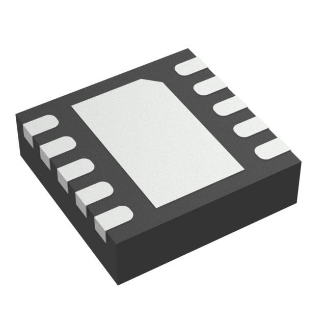
10-Pin SON (3-mm × 3-mm) Package with
Wettable Flanks
The power-switch rise and fall times are controlled to
minimize current surges during turn on or off. The
FAULT logic output asserts low during overcurrent or
overtemperature conditions.
Device Information(1)
2 Applications
•
•
PART NUMBER
Automotive USB Ports/Hubs
Automotive Internal Load Switch
TPS2559-Q1
PACKAGE
VSON (10)
BODY SIZE (NOM)
3.00mm x 3.00mm
(1) For all available packages, see the orderable addendum at
the end of the datasheet.
Simplified Schematic
TPS2559 -Q1DRC
2.5V-6.5V
0.1PF
2/3/ 4
FAULT
Signal
IN
OUT
VOUT
7/8/ 9
COUT
RFAULT
10
Control
Signal
FAULT
ILIM
5
EN
Power
PAD
GND
6
R ILIM
1
1
An IMPORTANT NOTICE at the end of this data sheet addresses availability, warranty, changes, use in safety-critical applications,
intellectual property matters and other important disclaimers. PRODUCTION DATA.
�TPS2559-Q1
SLVSD03 – DECEMBER 2015
www.ti.com
Table of Contents
1
2
3
4
5
6
7
8
9
Features ..................................................................
Applications ...........................................................
Description .............................................................
Revision History.....................................................
Device Comparison Table.....................................
Pin Configuration and Functions .........................
Specifications.........................................................
1
1
1
2
3
3
4
7.1
7.2
7.3
7.4
7.5
7.6
7.7
4
4
4
4
5
6
7
Absolute Maximum Ratings ......................................
ESD Ratings ............................................................
Recommended Operating Conditions.......................
Thermal Information ..................................................
Electrical Characteristics...........................................
Timing Requirements ...............................................
Typical Characteristics ..............................................
9.2 Functional Block Diagram ....................................... 10
9.3 Feature Description................................................. 10
9.4 Device Functional Modes........................................ 11
10 Application and Implementation........................ 12
10.1 Application Information.......................................... 12
10.2 Typical Application ............................................... 12
11 Power Supply Recommendations ..................... 19
12 Layout................................................................... 20
12.1 Layout Guidelines ................................................. 20
12.2 Layout Example .................................................... 20
13 Device and Documentation Support ................. 21
13.1
13.2
13.3
13.4
Parameter Measurement Information .................. 9
Detailed Description ............................................ 10
Community Resources..........................................
Trademarks ...........................................................
Electrostatic Discharge Caution ............................
Glossary ................................................................
21
21
21
21
14 Mechanical, Packaging, and Orderable
Information ........................................................... 21
9.1 Overview ................................................................. 10
4 Revision History
2
DATE
REVISION
NOTES
December 2015
*
Initial release.
Submit Documentation Feedback
Copyright © 2015, Texas Instruments Incorporated
Product Folder Links: TPS2559-Q1
�TPS2559-Q1
www.ti.com
SLVSD03 – DECEMBER 2015
5 Device Comparison Table
Device
Operation
Range (V)
OCP Mode
ICONT.
Adj. Range (A)
TPS2559-Q1
2.5 - 6.5
Auto Retry
TPS2553-Q1
2.5 - 6.5
Auto Retry
TPS2556/7-Q1
2.5 - 6.5
TPS2561A-Q1
(Dual Channels)
TPS25200-Q1
(With OVP protection)
RDS(on) (mΩ)
IOS tolerance
Package
5.5
13
±4.7% at 4.7 A
DRC (SON-10)
1.2
85 (DBV)
±6.8% at 1.3 A
DBV (SOT-23)
Auto Retry
5
22
±6.3% at 4.5 A
DRB (SON-8)
2.5 - 6.5
Auto Retry
2.5
44
2.1 A to 2.5 A
DRC (SON-10)
2.5 - 6.5
(Withstand up to 20V)
Auto Retry
2.5
60
±6.3% at 2.7 A
DRV (SON-6)
6 Pin Configuration and Functions
DRC Package
SON-10 (10 Pins)
Top View
GND
IN
IN
IN
EN
1
2
3
4
5
10
9
PAD 8
7
6
FAULT
OUT
OUT
OUT
ILIM
Pin Functions
PIN
NAME
GND
NO.
TYPE
1
DESCRIPTION
Ground connection, connect externally to PowerPAD
IN
2,3,4
I
Input voltage, connect a 0.1 μF or greater ceramic capacitor from IN to GND as close to the
IC as possible
EN
5
I
Enable input, logic high turns on power switch.
ILIM
6
O
External resistor used to set current-limit threshold; recommended. 24.9 kΩ ≤ R(ILIM) ≤ 100
kΩ.
OUT
7,8,9
O
Power-switch output
10
O
Active-low open-drain output, asserted during over-current or overtemperature conditions.
FAULT
PowerPAD™
PAD
Internally connected to GND; used to heat-sink the part to the circuit board traces. Connect
PowerPAD to GND pin externally.
Submit Documentation Feedback
Copyright © 2015, Texas Instruments Incorporated
Product Folder Links: TPS2559-Q1
3
�TPS2559-Q1
SLVSD03 – DECEMBER 2015
www.ti.com
7 Specifications
7.1 Absolute Maximum Ratings
over operating free-air temperature range (unless otherwise noted)
Voltage range
(1) (2)
IN, OUT, EN, ILIM, FAULT
IN to OUT
Continuous output current, IOUT
OUT
MIN
MAX
UNIT
–0.3
7
V
–7
7
V
Internally Limited
Continuous FAULT sink current
mA
20
ILIM source current
mA
Internally Limited
mA
Maximum junction temperature, TJ
–40
to OTSD2
°C
Storage temperature, Tstg
–65
150
°C
(1)
(2)
Stresses beyond those listed under Absolute Maximum Ratings may cause permanent damage to the device. These are stress ratings
only, which do not imply functional operation of the device at these or any other conditions beyond those indicated under Recommended
Operating Conditions. Exposure to absolute-maximum-rated conditions for extended periods may affect device reliability.
Voltages are referenced to GND unless otherwise noted.
7.2 ESD Ratings
VALUE
Human body model (HBM), ESD stress voltage, all pins
Electrostatic
discharge (1)
V(ESD)
(2)
(3)
(4)
(4)
UNIT
±2000
Charged device model (CDM), ESD stress voltage, all pins (3)
System Level
(1)
(2)
±750
Contact discharge
±8000
Air discharge
±15000
V
Electrostatic discharge (ESD) to measure device sensitivity or immunity to damage caused by assembly-line electrostatic discharges
into the device.
The passing level per AEC-Q100 Classification H2.
The passing level per AEC-Q100 Classification C5.
Surges per EN61000-4-2, 1999 applied between USB and output ground of the TPS2559EVM (SLUUB15) evaluation module
(documentation available on the Web.) These were the test levels, not the failure threshold.
7.3 Recommended Operating Conditions
over operating free-air temperature range (unless otherwise noted)
VIN
Input voltage, IN
VEN
Input voltage, EN
IOUT
Continuous output current of OUT
MIN
MAX
2.5
6.5
V
0
6.5
V
5.5
A
Continuous FAULT sink current
R(ILIM)
Recommended resistor limit range
TJ
Operating junction temperature
(1)
(1)
UNIT
10
mA
24.9
100
kΩ
-40
125
°C
R(ILIM) is the resistor from ILIM pin to GND and ILIM pin can be shorted to GND.
7.4 Thermal Information
THERMAL METRIC (1)
TPS2559-Q1
DRC (10 PINS)
UNIT
RθJA
Junction-to-ambient thermal resistance
40.6
°C/W
RθJC(top)
Junction-to-case (top) thermal resistance
45.5
°C/W
RθJB
Junction-to-board thermal resistance
15.9
°C/W
ψJT
Junction-to-top characterization parameter
0.4
°C/W
ψJB
Junction-to-board characterization parameter
15.7
°C/W
RθJC(bot)
Junction-to-case (bottom) thermal resistance
2.8
°C/W
(1)
4
For more information about traditional and new thermal metrics, see the IC Package Thermal Metrics application report, SPRA953.
Submit Documentation Feedback
Copyright © 2015, Texas Instruments Incorporated
Product Folder Links: TPS2559-Q1
�TPS2559-Q1
www.ti.com
SLVSD03 – DECEMBER 2015
7.5 Electrical Characteristics
Conditions are –40°C ≤ TJ ≤ 125°C, 2.5 V ≤ VIN ≤ 6.5 V, V(EN) = VIN, R(ILIM) = 49.9 kΩ. Positive current are into pins. Typical
value is at 25°C. All voltages are with respect to GND (unless otherwise noted).
PARAMETER
TEST CONDITIONS
MIN
TYP
MAX
13
16
UNIT
POWER SWITCH
RDS(on)
TJ = 25°C
Input - Output Resistance (1)
-40°C ≤ TJ ≤ 125°C
21
mΩ
ENABLE INPUT EN
EN turn on/off threshold
0.66
Hysteresis
I(EN)
1.1
55
Input current
V(EN) = 0 V or V(EN) = 6.5 V
(2)
–1
V
mV
1
µA
CURRENT LIMIT
IOS
OUT short circuit current limit
R(ILIM) = 24.9 kΩ
4490
4730
4931
R(ILIM) = 44.2kΩ
2505
2660
2805
R(ILIM) = 49.9kΩ
2215
2360
2490
R(ILIM) = 61.9 kΩ
1780
1900
2015
R(ILIM) = 100 kΩ
1080
1180
1265
ILIM pin short to GND (R(ILIM) = 0)
5860
6700
7460
mA
SUPPLY CURRENT
I(IN_OFF) Disabled, IN supply current
V(EN) = 0 V, No load on OUT
0.1
2
R(ILIM) = 100 kΩ, no load on OUT
97
125
R(ILIM) = 24.9 kΩ, no load on OUT
107
135
VOUT = 6.5 V, VIN = 0 V, TJ = 25°C,
Measure IOUT
0.01
1
IN rising UVLO threshold voltage
2.36
2.45
Hysteresis
35 (2)
I(IN_ON)
Enabled, IN supply current
I(REV)
Reverse leakage current
µA
µA
µA
UNDERVOLTAGE LOCKOUT
VUVLO
V
mV
FAULT
VOL
Output low voltage
IFAULT = 1 mA
Off-state leakage
VFAULT = 6.5 V
180
mV
1
µA
THERMAL SHUTDOWN
OTSD2
Thermal shutdown threshold
155
OTSD1
Thermal shutdown threshold in current-limit
135
Hysteresis
(1)
(2)
°C
20
(2)
Pulse-testing techniques maintain junction temperature close to ambient temperature. Thermal effects must be taken into account
separately
These parameters are provided for reference only, and don’t constitute part of TI’s published device specifications for purposes of TI’s
product warranty.
Submit Documentation Feedback
Copyright © 2015, Texas Instruments Incorporated
Product Folder Links: TPS2559-Q1
5
�TPS2559-Q1
SLVSD03 – DECEMBER 2015
www.ti.com
7.6 Timing Requirements
Conditions are –40°C ≤ TJ = ≤ 125°C, 2.5 V ≤ VIN ≤ 6.5 V, V(EN) = VIN, R(ILIM) = 49.9 kΩ. Positive current are into pins. Typical
value is at 25°C. All voltages are with respect to GND (unless otherwise noted).
PARAMETER
TEST CONDITIONS
MIN
TYP
MAX
VIN = 6.5 V
2.6
3.44
5.2
VIN = 2.5 V
1.3
2.01
3.9
0.7
0.89
1.3
0.42
0.58
1.04
UNIT
POWER SWITCH
tr
tf
OUT voltage rise time
OUT voltage fall time
VIN = 6.5 V
CL = 1 µF, RL = 100 Ω, See Figure 13
VIN = 2.5 V
ms
ENABLE INPUT EN
ton
OUT voltage turn-on time
toff
OUT voltage turn-off time
15
CL = 1 µF, RL = 100 Ω, See Figure 14
8
ms
CURRENT LIMIT
tIOS
Short-circuit response time (1)
3.5 (1)
VIN = 5 V, RSHORT = 50 mΩ, See Figure 15
µs
FAULT
FAULT deglitch
(1)
6
FAULT assertion or de-assertion due to overcurrent
condition
6
9
13
ms
This parameter is provided for reference only and does not constitute part of TI's published device specifications for purposes of TI's
product warranty
Submit Documentation Feedback
Copyright © 2015, Texas Instruments Incorporated
Product Folder Links: TPS2559-Q1
�TPS2559-Q1
www.ti.com
SLVSD03 – DECEMBER 2015
7.7 Typical Characteristics
0.6
0.5
2.4
0.4
IIN_OFF ( A)
Undervoltage Lockout (V)
2.5
2.3
2.2
0.3
0.2
2.1
0.1
Rising
Falling
2.0
±50
0
50
100
0.0
±50
150
Junction Temperature (ƒC)
0
50
100
150
Junction Temperature (ƒC)
C001
C002
VIN = 6.5 V
Figure 2. Supply Current, Output Disabled (IIN_OFF) vs
Temperature
Figure 1. Under-voltage Lockout (UVLO) vs Temperature
120
140
100
120
100
IIN_ON ( A)
IIN_ON ( A)
80
60
40
80
60
40
20
V
VIN=2.5
IN = 2.5 V
VIN=6.5
V
IN = 6.5 V
0
±50
0
50
100
Junction Temperature (ƒC)
V
VIN=2.5
IN = 2.5 V
20
VIN=6.5
V
IN = 6.5 V
0
150
±50
0
100
Junction Temperature (ƒC)
C003
R(ILIM) = 100 KΩ
50
150
C004
R(ILIM) = 24.9 KΩ
Figure 3. Supply Current, Output Enabled (IIN_ON) vs
Temperature
Figure 4. Supply Current, Output Enabled (IIN_ON) vs
Temperature
0.7
18
0.6
16
RDS(on) (m )
IREV ( A)
0.5
0.4
0.3
0.2
0.1
14
12
10
0.0
8
±0.1
±50
0
50
100
Junction Temperature (ƒC)
150
±50
VOUT = 6.5 V
0
50
100
Junction Temperature (ƒC)
C005
150
C006
VIN = 5 V
Figure 5. Reverse Leakage Current (IREV) v. Temperature
Figure 6. Input-Output Resistance (RDS(on)) vs Temperature
Submit Documentation Feedback
Copyright © 2015, Texas Instruments Incorporated
Product Folder Links: TPS2559-Q1
7
�TPS2559-Q1
SLVSD03 – DECEMBER 2015
www.ti.com
Typical Characteristics (continued)
8.0
13
7.5
12
11
tFAULT (ms)
IOS (A)
7.0
6.5
10
9
6.0
8
5.5
7
5.0
6
±50
0
50
100
150
Junction Temperature (ƒC)
VIN = 6.5 V
50
100
150
Junction Temperature (ƒC)
ILIM pin short to GND
C008
V(FAULT) = 2.5 V
Figure 7. Short Circuit Current (IOS) vs Temperature
Figure 8. Deglitch Time (tFAULT) vs Temperature
4.0
1.0
3.5
0.9
0.8
3.0
0.7
tF (ms)
2.5
tR (ms)
0
±50
C007
2.0
1.5
0.6
0.5
0.4
0.3
1.0
0.2
V
VIN=2.5
IN = 2.5 V
0.5
0.0
±50
0
50
100
COUT = 1 µF
VVIN=6.5V
IN = 6.5 V
0.0
150
Junction Temperature (ƒC)
VVIN=2.5V
IN = 2.5 V
0.1
VIN=6.5
V
IN = 6.5 V
50
100
Junction Temperature (ƒC)
R(LOAD) = 100 Ω
150
C010
R(LOAD) = 100 Ω
COUT = 1 µF
Figure 9. Output Rise Time (tR) vs Temperature
Figure 10. Output Fall Time (tF) vs Temperature
6
R
24.9
k
RILIM
24.9K
ILIM = =
R
RILIM=44.2K
ILIM = 44.9 k
R
RILIM=49.9K
ILIM = 49.9 k
R
RILIM=61.9K
ILIM = 61.9 k
R
RILIM=100K
ILIM = 100 k
5
4
IOS (A)
0
±50
C009
3
2
1
0
0
±50
50
100
Junction Temperature (ƒC)
150
C011
VIN = 6.5 V
Figure 11. Short Circuit Current (IOS) vs Temperature
8
Submit Documentation Feedback
Copyright © 2015, Texas Instruments Incorporated
Product Folder Links: TPS2559-Q1
�TPS2559-Q1
www.ti.com
SLVSD03 – DECEMBER 2015
8 Parameter Measurement Information
OUT
90%
RL
VOUT
CL
tf
tr
10%
Figure 12. Output Rise/Fall time Test Load
Figure 13. Power-On and Off Timing
spacer
spacer
VEN
50%
ton
IOUT
50%
toff
90%
VOUT
120% x IOS
IOS
0A
tIOS
10%
Figure 14. Enable Timing, Active High Enable
Figure 15. Output Short Circuit Parameters
Submit Documentation Feedback
Copyright © 2015, Texas Instruments Incorporated
Product Folder Links: TPS2559-Q1
9
�TPS2559-Q1
SLVSD03 – DECEMBER 2015
www.ti.com
9 Detailed Description
9.1 Overview
The TPS2559-Q1 is a current-limited, power-distribution switch using N-channel MOSFETs for applications
where short circuits or heavy capacitive loads will be encountered. This device allows the user to program the
current-limit via an external resistor and the maximum continuous output current up to 5.5 A. This device
incorporates an internal charge pump and the gate drive circuitry necessary to drive the N-channel MOSFET.
The charge pump supplies power to the driver circuit and provides the necessary voltage to pull the gate of the
MOSFET above the source. The charge pump operates from input voltages as low as 2.5 V and requires little
supply current. The driver controls the gate voltage of the power switch. The driver incorporates circuitry that
controls the rise and fall times of the output voltage to limit large current and voltage surges and provides built-in
soft-start functionality. The TPS2559-Q1 limits the output current to the programmed current-limit threshold IOS
during an overcurrent or short-circuit event by reducing the charge pump voltage driving the N-channel MOSFET
and operating it in the linear range of operation. The result of limiting the output current to IOS reduces the output
voltage at OUT because N-channel MOSFET is no longer fully enhanced.
9.2 Functional Block Diagram
IN
2/ 3/4
Current
Sense
Charge
Pump
EN
CS
7/8/ 9
Current
Limit
Driver
5
10
UVLO
ILIM
6
GND
1
OUT
Thermal
Sense
FAULT
9-ms
Deglitch
9.3 Feature Description
9.3.1 Thermal Sense
The TPS2559-Q1 self protects by using two independent thermal sensing circuits that monitor the operating
temperature of the power switch and disable operation if the temperature exceeds recommended operating
conditions. The TPS2559-Q1 device operates in constant-current mode during an over-current condition, which
increases the voltage drop across power switch. The power dissipation in the package is proportional to the
voltage drop across the power switch, which increases the junction temperature during an over-current condition.
The first thermal sensor (OTSD1) turns off the power switch when the die temperature exceeds 135°C (min) and
the part is in current limit. Hysteresis is built into the thermal sensor, and the switch turns on after the device has
cooled approximately 20°C.
The TPS2559-Q1 also has a second ambient thermal sensor (OTSD2). The ambient thermal sensor turns off the
power switch when the die temperature exceeds 155°C (min) regardless of whether the power switch is in
current limit and will turn on the power switch after the device has cooled approximately 20°C. The TPS2559-Q1
continues to cycle off and on until the fault is removed.
10
Submit Documentation Feedback
Copyright © 2015, Texas Instruments Incorporated
Product Folder Links: TPS2559-Q1
�TPS2559-Q1
www.ti.com
SLVSD03 – DECEMBER 2015
Feature Description (continued)
9.3.2 Overcurrent Protection
The TPS2559-Q1 responds to overcurrent conditions by limiting their output current to IOS. When an overload
condition is present, the device maintains a constant output current, with the output voltage determined by (IOS ×
RLOAD). Two possible overload conditions can occur.
The first condition is when a short circuit or partial short circuit is present when the device is powered-up or
enabled. The output voltage is held near zero potential with respect to ground and the TPS2559-Q1 ramps the
output current to IOS. The TPS2559-Q1 limits the current to IOS until the overload condition is removed or the
device begins to thermal cycle (see Figure 24).
The second condition is when a short circuit, partial short circuit, or transient overload occurs while the device is
enabled and powered on. The device responds to the overcurrent condition within time tIOS (see Figure 15). The
response speed and shape will vary with the overload level, input circuit, and rate of application. The current-limit
response will vary between simply settling to IOS, or turnoff and controlled return to IOS. Similar to the previous
case, the TPS2559-Q1 limits the current to IOS until the overload condition is removed or the device begins to
thermal cycle.
The TPS2559-Q1 thermal cycles if an overload condition is present long enough to activate thermal limiting in
any of the above cases. The device turns off when the junction temperature exceeds 135°C (min) while in current
limit. The device remains off until the junction temperature cools 20°C (typ) and then restarts. The TPS2559-Q1
cycles on/off until the overload is removed (see Figure 25).
9.3.3 FAULT Response
The FAULT open-drain output is asserted (active low) during an over-current or over-temperature condition. The
TPS2559-Q1 asserts the FAULT signal until the fault condition is removed and the device resumes normal
operation. The TPS2559-Q1 is designed to eliminate false FAULT reporting by using an internal delay "deglitch"
circuit for over-current (9-ms typ.) conditions without the need for external circuitry. This ensures that FAULT is
not accidentally asserted due to normal operation such as starting into a heavy capacitive load. The deglitch
circuitry delays entering and leaving current-limit induced fault conditions. The FAULT signal is not deglitched
when the MOSFET is disabled due to an over-temperature condition but is deglitched after the device has cooled
and begins to turn on. This unidirectional deglitch prevents FAULT oscillation during an over-temperature event.
9.4 Device Functional Modes
9.4.1 Operation with VIN Undervoltage Lockout (UVLO) Control
The undervoltage lockout (UVLO) circuit disables the power switch until the input voltage reaches the UVLO turnon threshold. Built-in hysteresis prevents unwanted on/off cycling due to input voltage droop during turn on.
9.4.2 Operation with EN Control
The logic enable controls the power switch and device supply current. The supply current is reduced to less than
2-μA when a logic low is present on EN. A logic high input on EN enables the driver, control circuits, and power
switch. The enable input is compatible with both TTL and CMOS logic levels.
Submit Documentation Feedback
Copyright © 2015, Texas Instruments Incorporated
Product Folder Links: TPS2559-Q1
11
�TPS2559-Q1
SLVSD03 – DECEMBER 2015
www.ti.com
10 Application and Implementation
NOTE
Information in the following applications sections is not part of the TI component
specification, and TI does not warrant its accuracy or completeness. TI’s customers are
responsible for determining suitability of components for their purposes. Customers should
validate and test their design implementation to confirm system functionality.
10.1 Application Information
The TPS2559-Q1 current limited power switch uses N-channel MOSFETs in applications requiring up to 5.5 A of
continuous load current. The device enters constant-current mode when the load exceeds the current limit
threshold.
The TPS2559-Q1 power switch is used to protect the up-stream power supply when the output is overloaded.
10.2 Typical Application
TPS2559 -Q1
5V
0.1PF
2/ 3/4
Fault
Signal
OUT
IN
VOUT
7/ 8/9
150µF
10kŸ
10
FAULT
5
EN
ILIM
Control
Signal
Power
Pad
6
GND
RILIM *
1
Figure 16. Typical TPS2559-Q1 Power Switch
Use the IOS in the Electrical Characteristics table or IOS in Equation 1 to select the RILIM.
10.2.1 Design Requirements
For this design example, use the following as the input parameters.
DESIGN PARAMETERS
EXAMPLE VALUE
Input Operation Voltage
5V
Rating Current
3A or 4.5A
Minimum Current Limit
3A
Maximum Current Limit
5A
When choose power switch, there are some several general steps:
1. What is the power rail, 3.3 V or 5 V, and then choose the operation range of power switch can cover the
power rail.
2. What is the normal operation current, for example, the maximum allowable current drawn by portable
equipment for USB 2.0 port is 500mA, so the normal operation current is 500mA and the minimum current
limit of power switch must exceed 500 mA to avoid false trigger during normal operation.
3. What is the maximum allowable current provided by up-stream power, and then decide the maximum current
limit of power switch that must lower it to ensure power switch can protect the up-stream power when overload is encountered at the output of power switch.
12
Submit Documentation Feedback
Copyright © 2015, Texas Instruments Incorporated
Product Folder Links: TPS2559-Q1
�TPS2559-Q1
www.ti.com
SLVSD03 – DECEMBER 2015
NOTE
Choosing power switch with tighter current limit tolerance can loosen the up-stream power
supply design.
10.2.2 Detailed Design Procedure
10.2.2.1 Step by Step Design Procedure
To
•
•
•
•
begin the design process a few parameters must be decided upon. The designer needs to know the following:
Normal Input Operation Voltage
Rating Current
Minimum Current Limit
Maximum Current Limit
10.2.2.2 Input and Output Capacitance
Input and output capacitance improves the performance of the device; the actual capacitance should be
optimized for the particular application. For all applications, a 0.1μF or greater ceramic bypass capacitor between
IN and GND is recommended as close to the device as possible for local noise decoupling. This precaution
reduces ringing on the input due to power-supply transients. Additional input capacitance may be needed on the
input to reduce voltage undershoot from exceeding the UVLO of other load share one power rail with TPS2559Q1 or overshoot from exceeding the absolute-maximum voltage of the device during heavy transient conditions.
This is especially important during bench testing when long, inductive cables are used to connect the evaluation
board to the bench power supply.
Output capacitance is not required, but placing a high-value electrolytic capacitor on the output pin is
recommended when large transient currents are expected on the output to reduce the undershoot, which caused
by the inductance of the output power bus just after a short has occurred and the TPS2559-Q1 has abruptly
reduced OUT current. Energy stored in the inductance will drive the OUT voltage down and potentially negative
as it discharges.
10.2.2.3 Programming the Current-Limit Threshold
The overcurrent threshold is user programmable via an external resistor. The TPS2559-Q1 uses an internal
regulation loop to provide a regulated voltage on the ILIM pin. The current-limit threshold is proportional to the
current sourced out of ILIM. The recommended 1% resistor range for R(ILIM) is 24.9 kΩ ≤ R(ILIM) ≤ 100 kΩ to
ensure stability of the internal regulation loop.
When ILIM pin short to GND (single point failure), maximum current limit is less than 8 A over temperature and
process variation.
Many applications require that the minimum current limit is above a certain current level or that the maximum
current limit is below a certain current level, so it is important to consider the tolerance of the overcurrent
threshold when selecting a value for R(ILIM). The equations and the graph below can be used to estimate the
minimum and maximum variation of the current-limit threshold for a predefined resistor value within R(ILIM) is 24.9
kΩ ≤ R(ILIM) ≤ 100 kΩ. This variation is an approximation only and does not take into account, for example, the
resistor tolerance. For examples of more-precise variation of IOS refer to the current-limit section of the Electrical
Characteristics table.
118848 V
IOSmax (mA) =
+ 30
R(ILIM)0.9918kW
IOSnom (mA) =
IOSmin (mA) =
118079 V
R(ILIM)1.0008kW
113325 V
R(ILIM)1.0010kW
- 47
(1)
24.9 kΩ ≤ R(ILIM) ≤ 100 kΩ
Submit Documentation Feedback
Copyright © 2015, Texas Instruments Incorporated
Product Folder Links: TPS2559-Q1
13
�TPS2559-Q1
SLVSD03 – DECEMBER 2015
www.ti.com
6000
IIos(Min)
OS (Min)
IOS (Typ)
IOS (Max)
Current Limit Threshold (mA)
5500
5000
4500
4000
3500
3000
2500
2000
1500
1000
500
0
20
30
40
50
60
70
80
Current Limit Resistor (k
90
100
C012
Figure 17. Current-Limit vs R(ILIM)
10.2.2.4 Design Above a Minimum Current Limit
Some applications require that current limiting cannot occur below a certain threshold. For this example, assume
that 3 A must be delivered to the load so that the minimum desired current-limit threshold is 3000 mA. Use the
IOS equations and Figure 17 to select R(ILIM).
IOSmin (mA) = 3000 mA
113325 V
IOSmin (mA) =
- 47
R(ILIM)1.0010kW
1
1
æ 113325 ö 1.0010 æ 113325 ö 1.0010
R(ILIM) (kW) = ç
=ç
= 37.06 kW
÷
÷
ç IOS(min) + 47 ÷
è 3000 + 47 ø
è
ø
(2)
Select the closest 1% resistor less than the calculated value: R(ILIM) = 36.5 kΩ. This sets the minimum currentlimit threshold at 3016 A.
113325 V
113325
- 47 =
- 47 = 3016 mA
IOSmin (mA) =
1.0010
R(ILIM)
kW
(36.5 ´ 1.01)1.0010
(3)
Use the IOS equations, Figure 17, and the previously calculated value for R(ILIM) to calculate the maximum
resulting current-limit threshold.
118848
118848
IOSmax (mA) =
+ 30 =
+ 30 = 3417 mA
0.9918
R(ILIM)
(36.5 ´ 0.99)0.9918
(4)
The resulting maximum current-limit threshold minimum is 3016 mA and maximum is 3417 mA with a 36.5 kΩ ±
1%.
10.2.2.5 Design Below a Maximum Current Limit
Some applications require that current limiting must occur below a certain threshold. For this example, assume
that 5A must be delivered to the load so that the minimum desired current-limit threshold is 5000 mA. Use the IOS
equations and Figure 17 to select R(ILIM).
IOSmax (mA) = 5000 mA
IOSmax (mA) =
118848
R(ILIM)0.9918kW
+ 30
1
1
æ 118848 ö 0.9918 æ 118848 ö 0.9918
R(ILIM) (kW) = ç
=ç
= 24.55 kW
÷
÷
ç IOS(max) - 30 ÷
è 5000 - 30 ø
è
ø
14
Submit Documentation Feedback
(5)
Copyright © 2015, Texas Instruments Incorporated
Product Folder Links: TPS2559-Q1
�TPS2559-Q1
www.ti.com
SLVSD03 – DECEMBER 2015
Select the closest 1% resistor less than the calculated value: RILIM = 24.9 kΩ. This sets the maximum currentlimit threshold at 4950 A.
118848
118848
+ 30 =
+ 30 = 4980 mA
IOSmax (mA) =
0.9918
R(ILIM)
kW
(24.9 ´ 0.99 )0.9918
(6)
Use the IOS equations, Figure 17, and the previously calculated value for R(ILIM) to calculate the minimum
resulting current-limit threshold.
113325
113325
IOSmin (mA) =
- 47 =
- 47 = 4445 mA
1.0010
R(ILIM)
(24.9 ´ 1.01)1.0010
(7)
The resulting minimum current-limit threshold minimum is 4445 mA and maximum is 4980 mA with a 24.9 kΩ ±
1%.
10.2.2.6 Accounting for Resistor Tolerance
The previous sections described the selection of R(ILIM) given certain application requirements and the
importance of understanding the current-limit threshold tolerance. The analysis focused only on the TPS2559-Q1
is bounded by an upper and lower tolerance centered on a nominal resistance. The additional RILIM resistance
tolerance directly affects the current-limit threshold accuracy at a system level. Table 1 shows a process that
accounts for worst-case resistor tolerance assuming 1% resistor values.
Step one follows the selection process outlined in the application examples above.
Step two determines the upper and lower resistance bounds of the selected resistor.
Step three uses the upper and lower resistor bounds in the IOS equations to calculate the threshold limits.
It is important to use tighter tolerance resistors, that is, 0.5% or 0.1%, when precision current limiting is desired.
Table 1. Common R(ILIM) Resistor Selections
DESIRED NOMINAL
CURRENT LIMIT
(mA)
IDEAL
RESISTOR
(kΩ)
CLOSEST 1%
RESISTOR
(kΩ)
1250
94.1
1500
1750
RESISTOR TOLERANCE
ACTUAL LIMITS
1% LOW
(kΩ)
1% HIGH
(kΩ)
IOS MIN
(mA)
IOS NOM
(mA)
IOS MAX
(mA)
93.1
92.2
94
1152.7
1263.7
1368.2
78.4
78.7
77.9
79.5
1372.5
1495.1
1610.9
67.2
66.5
65.8
67.2
1633.2
1769.7
1893.3
2000
58.8
59
58.4
59.6
1847
1994.8
2133.7
2250
52.3
52.3
51.8
52.8
2089.9
2550.6
2400.9
2500
47.1
47.5
47
48
2306
2478.2
2638.4
2750
42.8
43.2
42.8
43.6
2540.5
2725.1
2895.8
3000
39.2
39.2
38.8
39.6
2804.8
3003.4
3185.7
3250
36.2
36.5
36.1
36.9
3016
3225.7
3417.2
3500
33.6
34
33.7
34.3
3241.4
3463.1
3664.1
3750
31.4
31.6
31.3
31.9
3491.5
3726.4
3937.8
4000
29.4
29.4
29.1
29.7
3756.5
4005.4
4227.7
4250
27.7
28
27.7
28.3
3946.9
4205.9
4435.8
4500
26.2
26.1
25.8
26.4
4237.9
4512.3
4753.9
4750
24.8
24.9
24.7
25.1
4444.6
4729.9
4979.6
Submit Documentation Feedback
Copyright © 2015, Texas Instruments Incorporated
Product Folder Links: TPS2559-Q1
15
�TPS2559-Q1
SLVSD03 – DECEMBER 2015
www.ti.com
10.2.2.7 Power Dissipation and Junction Temperature
The low on-resistance of the N-channel MOSFET allows small surface-mount packages to pass large currents. It
is good design practice to estimate power dissipation and junction temperature. The below analysis gives an
approximation for calculating junction temperature based on the power dissipation in the package. However, it is
important to note that thermal analysis is strongly dependent on additional system level factors. Such factors
include air flow, board layout, copper thickness and surface area, and proximity to other devices dissipating
power. Good thermal design practice must include all system level factors in addition to individual component
analysis. Begin by determining the rDS(on) of the N-channel MOSFET relative to the input voltage and operating
temperature. As an initial estimate, use the highest operating ambient temperature of interest and read rDS(on)
from the typical characteristics graph. Using this value, the power dissipation can be calculated using Equation 8:
PD = rDS(on) × IOUT2
(8)
Where:
PD = Total power dissipation (W)
rDS(on) = Power switch on-resistance (Ω)
IOUT = Maximum current-limit threshold (A)
This step calculates the total power dissipation of the N-channel MOSFET.
Finally, calculate the junction temperature:
TJ = PD × θJA + TA
(9)
Where:
TA = Ambient temperature (°C)
θJA = Thermal resistance (°C/W)
PD = Total power dissipation (W)
Compare the calculated junction temperature with the initial estimate. If they are not within a few degrees, repeat
the calculation using the "refined" rDS(on) from the previous calculation as the new estimate. Two or three
iterations are generally sufficient to achieve the desired result. The final junction temperature is highly dependent
on thermal resistance θJA and thermal resistance is highly dependent on the individual package and board
layout.
10.2.2.8 Auto-Retry
Some applications require that an overcurrent condition disables the part momentarily during a fault condition
and re-enables after a pre-set time. This auto-retry functionality can be implemented with an external resistor and
capacitor. During a fault condition, FAULT pulls low EN. The part is disabled when EN is pulled below the turn-off
threshold, and FAULT goes high impedance allowing C(RETRY) to begin charging. The part re-enables when the
voltage on EN reaches the turn-on threshold. The part will continue to cycle in this manner until the fault
condition is removed. The auto-retry cycling time is determined by the resistor/capacitor time constant, TPS2559Q1 turn on time and FAULT deglitch time (see Figure 28).
TPS2559-Q1
VIN
0.1PF
2/3/4
OUT
IN
VOUT
7/8/9
C OUT
R FAULT
100k:
10
FAULT
5
EN
ILIM
C RETRY
PF
Power
Pad
6
GND
100 kŸ
1
Figure 18. Auto-Retry Circuit
16
Submit Documentation Feedback
Copyright © 2015, Texas Instruments Incorporated
Product Folder Links: TPS2559-Q1
�TPS2559-Q1
www.ti.com
SLVSD03 – DECEMBER 2015
Some applications require auto-retry functionality and the ability to enable/disable with an external logic signal.
Figure 19 shows how an external logic signal can drive EN through R(FAULT) and maintain auto-retry functionality.
The resistor/capacitor time constant determines the auto-retry time-out period.
TPS2559 -Q1
VIN
0.1PF
2/ 3/4
OUT
IN
VOUT
7/ 8/9
C OUT
External Logic
Signal and Driver
10
R FAULT
100 k:
FAULT
ILIM
5
C RETRY
PF
EN
Power
Pad
6
GND
100kŸ
1
Figure 19. Auto-Retry Circuit with External EN Signal
If need to implement latch-off, refer to application report (SLVA282A).
10.2.2.9 Two-level Current-limit
Some applications require different current-limit thresholds depending on external system conditions. Figure 20
shows an implementation for an externally-controlled, two-level current-limit circuit. The current-limit threshold is
set by the total resistance from ILIM to GND (see previously discussed Programming the Current-Limit Threshold
section). A logic-level input enables/disables MOSFET Q1 and changes the current-limit threshold by modifying
the total resistance from ILIM to GND (see Figure 29 and Figure 30). Additional MOSFET/resistor combinations
can be used in parallel to Q1/R2 to increase the number of additional current-limit levels.
NOTE
ILIM should never be driven directly with an external signal.
TPS2559-Q1
5V
0.1PF
2/3/ 4
OUT
IN
VOUT
7/8/ 9
10kŸ
C OUT
10
FAULT
5
EN
ILIM
Control
Signal
Power
Pad
R1
100 kŸ
6
R2
100 kŸ
Current Limit
Control Signal
GND
1
Q1
Figure 20. Two-Level Current-Limit Circuit
Submit Documentation Feedback
Copyright © 2015, Texas Instruments Incorporated
Product Folder Links: TPS2559-Q1
17
�TPS2559-Q1
SLVSD03 – DECEMBER 2015
www.ti.com
10.2.3 Application Curves
6
3.0
6
5
2.5
5
3.0
V
VEN
EN
V
VOUT
OUT
2.5
3
1.5
2
1.0
1
4
2.0
3
1.5
2
1.0
0.5
1
0.5
0.0
0
0.0
±0.5
±1
IOUT (A)
2.0
VEN, VOUT (V)
4
IOUT (A)
VEN, VOUT (V)
IIOUT
OUT
V
VEN
EN
IIOUT
OUT
±1
±4
0
4
8
12
16
±0.5
0
±4
Time (ms)
3
2
2
VOUT , VFAULT (V)
3
6
VFAULT
Vfault
IIOUT
OUT
5
5
4
4
3
3
2
2
1
1
1
1
0
0
0
0
±1
±1
±8
0
8
16
24
±1
±40
32
Time (ms)
±20
0
20
40
60
80
100 120 140 160
Time (ms)
C015
C016
Figure 24. Full Load to Output Short Transient Response
Figure 23. Enable into Output Short
6
6
6
5
5
5
4
4
4
4
3
3
3
3
2
2
2
2
1
1
1
1
0
0
0
0
±1
±1
VFAULT
Vfault
±1
±80
±60
±40
±20
Time (ms)
0
20
VOUT (V)
6
Vout
V
OUT
IIout
OUT
IIOUT
OUT
IOUT (A)
V
VOUT
OUT
VOUT , VFAULT (V)
C014
V
VOUT
OUT
4
±1
5
±1
±2
C017
Figure 25. Output Short to Full Load Recovery Response
18
16
6
IOUT (A)
VEN, VFAULT (V)
4
12
Figure 22. Output Fall with 150µF // 5Ω
5
VEN
V
EN
Vfault
V
FAULT
IIOUT
OUT
8
Time (ms)
C013
Figure 21. Output Rise with 150µF // 5Ω
5
4
IOUT (A)
V
VOUT
OUT
IOUT (A)
0
Submit Documentation Feedback
0
2
4
6
Time (ms)
8
C019
Figure 26. 50mΩ Hot-Short
Copyright © 2015, Texas Instruments Incorporated
Product Folder Links: TPS2559-Q1
�TPS2559-Q1
SLVSD03 – DECEMBER 2015
3.0
1.2
50
2.5
1.0
2.0
0.8
1.5
0.6
1.0
0.4
0.5
0.2
4
40
3
30
2
20
1
10
0
0
±1
±2
±20
±5
±4
±3
±2
±1
0
1
2
3
4
0.0
0.0
±10
±0.5
5
±40
Time ( s)
0
40
80
Figure 27. 50mΩ Hot-Short Response Time
3
1.5
2
1.0
1
0.5
0.0
±1
±2.0
±1.5
±1.0
±0.5
0.0
Vfault
V
FAULT
0.5
1.0
VOUT ,VGATE, VFAULT (V)
2.0
IOUT (A)
VOUT ,VGATE, VFAULT (V)
4
V
Vgate
GATE
±0.2
200
240
280
320
360
C021
6
3.0
V
Vout
OUT
V
VOUT
OUT
160
Figure 28. Auto-Retry Cycle
2.5
0
120
IIOUT
OUT
Time (ms)
C020
5
VOUT
Vfault
VFAULT
VOUT
VFAULT
Vfault
VGATE
Vgate
IOUT
Iout
5
2.5
4
2.0
3
1.5
2
1.0
1
0.5
0
0.0
IOUT (A)
VOUT (V)
5
60
VOUT , VFAULT (V)
VOUT
VOUT
IOUT
IOUT
IOUT (A)
6
IOUT (A)
www.ti.com
IIOUT
OUT
±0.5
1.5
±1
±0.5 ±0.4 ±0.3 ±0.2 ±0.1
2.0
Time (s)
0.1
0.2
0.3
0.4
0.5
Time (s)
C022
Figure 29. Two Level Current Limit with RLOAD = 2.5 Ω
±0.5
0.0
C023
Figure 30. Two Level Current Limit with RLOAD = 1Ω
11 Power Supply Recommendations
Design of the devices is for operation from an input voltage supply range of 2.5 V to 6.5 V. The current capability
of the power supply should exceed the maximum current limit of the power switch.
Submit Documentation Feedback
Copyright © 2015, Texas Instruments Incorporated
Product Folder Links: TPS2559-Q1
19
�TPS2559-Q1
SLVSD03 – DECEMBER 2015
www.ti.com
12 Layout
12.1 Layout Guidelines
•
•
•
•
Place the 100-nF bypass capacitor near the IN and GND pins, and make the connections using a lowinductance trace.
Placing a high-value electrolytic capacitor and a 100-nF bypass capacitor on the output pin is recommended
when large transient currents are expected on the output.
The traces routing the RILIM resistor to the device should be as short as possible to reduce parasitic effects on
the current limit accuracy.
The PowerPAD should be directly connected to PCB ground plane using wide and short copper trace.
12.2 Layout Example
VIA to Power Ground Plane
Power Ground
High Frequency
Bypass Capacitor
IN
FAULT
1
108
2
9
3
8
4
7
5
6
OUT
ILIM
Figure 31. TPS2559-Q1 Board Layout
20
Submit Documentation Feedback
Copyright © 2015, Texas Instruments Incorporated
Product Folder Links: TPS2559-Q1
�TPS2559-Q1
www.ti.com
SLVSD03 – DECEMBER 2015
13 Device and Documentation Support
13.1 Community Resources
The following links connect to TI community resources. Linked contents are provided "AS IS" by the respective
contributors. They do not constitute TI specifications and do not necessarily reflect TI's views; see TI's Terms of
Use.
TI E2E™ Online Community TI's Engineer-to-Engineer (E2E) Community. Created to foster collaboration
among engineers. At e2e.ti.com, you can ask questions, share knowledge, explore ideas and help
solve problems with fellow engineers.
Design Support TI's Design Support Quickly find helpful E2E forums along with design support tools and
contact information for technical support.
13.2 Trademarks
PowerPAD, E2E are trademarks of Texas Instruments.
All other trademarks are the property of their respective owners.
13.3 Electrostatic Discharge Caution
These devices have limited built-in ESD protection. The leads should be shorted together or the device placed in conductive foam
during storage or handling to prevent electrostatic damage to the MOS gates.
13.4 Glossary
SLYZ022 — TI Glossary.
This glossary lists and explains terms, acronyms, and definitions.
14 Mechanical, Packaging, and Orderable Information
The following pages include mechanical, packaging, and orderable information. This information is the most
current data available for the designated devices. This data is subject to change without notice and revision of
this document. For browser-based versions of this data sheet, refer to the left-hand navigation.
Submit Documentation Feedback
Copyright © 2015, Texas Instruments Incorporated
Product Folder Links: TPS2559-Q1
21
�PACKAGE OPTION ADDENDUM
www.ti.com
10-Dec-2020
PACKAGING INFORMATION
Orderable Device
Status
(1)
Package Type Package Pins Package
Drawing
Qty
Eco Plan
(2)
Lead finish/
Ball material
MSL Peak Temp
Op Temp (°C)
Device Marking
(3)
(4/5)
(6)
TPS2559QWDRCRQ1
ACTIVE
VSON
DRC
10
3000
RoHS & Green
SN
Level-2-260C-1 YEAR
-40 to 125
2559Q
TPS2559QWDRCTQ1
ACTIVE
VSON
DRC
10
250
RoHS & Green
SN
Level-2-260C-1 YEAR
-40 to 125
2559Q
(1)
The marketing status values are defined as follows:
ACTIVE: Product device recommended for new designs.
LIFEBUY: TI has announced that the device will be discontinued, and a lifetime-buy period is in effect.
NRND: Not recommended for new designs. Device is in production to support existing customers, but TI does not recommend using this part in a new design.
PREVIEW: Device has been announced but is not in production. Samples may or may not be available.
OBSOLETE: TI has discontinued the production of the device.
(2)
RoHS: TI defines "RoHS" to mean semiconductor products that are compliant with the current EU RoHS requirements for all 10 RoHS substances, including the requirement that RoHS substance
do not exceed 0.1% by weight in homogeneous materials. Where designed to be soldered at high temperatures, "RoHS" products are suitable for use in specified lead-free processes. TI may
reference these types of products as "Pb-Free".
RoHS Exempt: TI defines "RoHS Exempt" to mean products that contain lead but are compliant with EU RoHS pursuant to a specific EU RoHS exemption.
Green: TI defines "Green" to mean the content of Chlorine (Cl) and Bromine (Br) based flame retardants meet JS709B low halogen requirements of


 工商网监
湘ICP备2023018690号
工商网监
湘ICP备2023018690号
