Sample &
Buy
Product
Folder
Support &
Community
Tools &
Software
Technical
Documents
TPS3702
SBVS251 – JANUARY 2015
TPS3702 High-Accuracy, Overvoltage and Undervoltage Monitor
1 Features
3 Description
•
•
The TPS3702 is an integrated overvoltage and
undervoltage window detector in a small SOT-6
package. This highly accuracy voltage monitor is
ideal for systems that operate on low-voltage supply
rails and have narrow margin supply tolerances. Low
threshold hysteresis options of 0.55% and 1.0%
prevent false reset signals when the monitored
voltage supply is in its normal range of operation.
Internal glitch immunity and noise filters further
eliminate false resets resulting from erroneous
signals.
1
•
•
•
•
•
•
•
Input Voltage Range: 2 V to 18 V
High Threshold Accuracy:
– 0.25% (typ)
– 0.9% (–40°C to 125°C)
Fixed Window Thresholds Optimized for Nominal
Rails Between 1 V and 5 V
Open-Drain Outputs for Overvoltage and
Undervoltage Indication
Internal Glitch Immunity
Threshold Adjust Using the SET Pin
Low Quiescent Current: 7 µA (typ)
Internal Threshold Hysteresis: 0.55%, 1.0%
SOT-6 Package
2 Applications
•
•
•
•
•
•
•
FPGA and ASIC Applications
DSP-Based Systems
Industrial Control Systems
Factory Automation
Personal Electronics
Building Automation
Motor Drives
The TPS3702 does not require any external resistors
for setting overvoltage and undervoltage reset
thresholds, which further increases overall accuracy
and reduces solution size and cost. The SET pin is
used to select between the two available threshold
voltages designed into each device. A separate
SENSE input pin and VDD pin allow for the
redundancy sought by safety-critical and highreliability systems. This device also features
independent reset outputs for the OV and UV pins; as
a result of the open-drain configuration, UV and OV
can be tied together.
This device has a low typical quiescent current
specification of 7 µA and is qualified for use over the
industrial temperature range of –40°C to 125°C.
Device Information(1)
Undervoltage Accuracy vs Temperature
0.5
Unit 1
Unit 4
0.4
Unit 2
Unit 5
Unit 3
Avg
PART NUMBER
UV Accuracy (%)
PACKAGE
TPS3702
0.3
0.2
BODY SIZE (NOM)
SOT (6)
2.90 mm × 1.60 mm
(1) For all available packages, see the orderable addendum at
the end of the datasheet.
0.1
0
-0.1
-0.2
Typical Application Circuit
-0.3
-0.4
Nominal Monitored Rail
Up to 5 V
-0.5
±40 ±25 ±10
5
20
35
50
65
80
95 110 125 140
Temperature (°C)
Overvoltage Accuracy vs Temperature
0.5
Unit 1
Unit 4
0.4
Unit 2
Unit 5
Unit 3
Avg
Up to
18 V
OV Accuracy (%)
0.3
0.2
TPS3702
0
R1
VDD
SENSE
0.1
R2
UV
RST
VDD
-0.1
Up to
6.5 V
-0.2
-0.3
GND
-0.4
µP
SET
OV
NMI
-0.5
±40 ±25 ±10
5
20
35
50
65
80
Temperature (°C)
95 110 125 140
C001
1
An IMPORTANT NOTICE at the end of this data sheet addresses availability, warranty, changes, use in safety-critical applications,
intellectual property matters and other important disclaimers. PRODUCTION DATA.
�TPS3702
SBVS251 – JANUARY 2015
www.ti.com
Table of Contents
1
2
3
4
5
6
7
Features ..................................................................
Applications ...........................................................
Description .............................................................
Revision History.....................................................
Pin Configuration and Functions .........................
Specifications.........................................................
1
1
1
2
3
4
6.1
6.2
6.3
6.4
6.5
6.6
6.7
4
4
4
4
5
6
7
Absolute Maximum Ratings ......................................
ESD Ratings..............................................................
Recommended Operating Conditions.......................
Thermal Information ..................................................
Electrical Characteristics...........................................
Timing Requirements ................................................
Typical Characteristics ..............................................
7.3 Feature Description................................................. 11
7.4 Device Functional Modes........................................ 12
8
Application and Implementation ........................ 13
8.1 Application Information............................................ 13
8.2 Typical Application ................................................. 17
9 Power Supply Recommendations...................... 19
10 Layout................................................................... 19
10.1 Layout Guidelines ................................................. 19
10.2 Layout Example .................................................... 19
11 Device and Documentation Support ................. 20
11.1
11.2
11.3
11.4
11.5
Detailed Description ............................................ 10
7.1 Overview ................................................................. 10
7.2 Functional Block Diagram ....................................... 10
Device Support......................................................
Documentation Support ........................................
Trademarks ...........................................................
Electrostatic Discharge Caution ............................
Glossary ................................................................
20
21
21
21
21
12 Mechanical, Packaging, and Orderable
Information ........................................................... 21
4 Revision History
2
DATE
REVISION
NOTES
January 2015
*
Initial release
Submit Documentation Feedback
Copyright © 2015, Texas Instruments Incorporated
Product Folder Links: TPS3702
�TPS3702
www.ti.com
SBVS251 – JANUARY 2015
5 Pin Configuration and Functions
DDC Package
SOT-6
(Top View)
UV
1
6
OV
GND
2
5
VDD
SENSE
3
4
SET
Pin Functions
PIN
I/O
DESCRIPTION
NO.
NAME
1
UV
O
Active-low, open-drain undervoltage output. This pin goes low when the SENSE voltage falls
below the internally set undervoltage threshold (VIT–). See the timing diagram in Figure 1 for
more details. Connect this pin to a pull-up resistor terminated to the desired pull-up voltage.
2
GND
—
Ground
3
SENSE
I
Input for the monitored supply voltage rail. When the SENSE voltage goes below the
undervoltage threshold, the UV pin is driven low.
When the SENSE voltage goes above the overvoltage threshold, the OV pin is driven low.
4
SET
I
Use this pin to configure the threshold voltages.
Refer to Table 3 for the desired configuration.
5
VDD
I
Supply voltage input pin. To power the device, connect a voltage supply (within the range of 2 V
and 18 V) to VDD.
Good analog design practice is to place a 0.1-μF ceramic capacitor close to this pin.
6
OV
O
Active-low, open-drain overvoltage output. This pin goes low when the SENSE voltage rises
above the internally set overvoltage threshold (VIT+). See the timing diagram in Figure 1 for more
details. Connect this pin to a pull-up resistor terminated to the desired pull-up voltage.
Submit Documentation Feedback
Copyright © 2015, Texas Instruments Incorporated
Product Folder Links: TPS3702
3
�TPS3702
SBVS251 – JANUARY 2015
www.ti.com
6 Specifications
6.1 Absolute Maximum Ratings
over operating free-air temperature range (unless otherwise noted) (1)
Voltage
Current
MIN
MAX
UNIT
VDD
–0.3
20
V
VUV, VOV
–0.3
20
V
VSENSE, VSET
–0.3
7
V
±40
mA
IUV, IOV
Continuous total power dissipation
Operating junction temperature, TJ
See the Thermal Information
(2)
Storage temperature, Tstg
(1)
(2)
–40
125
°C
–65
150
°C
Stresses beyond those listed under Absolute Maximum Ratings may cause permanent damage to the device. These are stress ratings
only, which do not imply functional operation of the device at these or any other conditions beyond those indicated under Recommended
Operating Conditions. Exposure to absolute-maximum-rated conditions for extended periods may affect device reliability.
As a result of the low dissipated power in this device, it is assumed that TJ = TA.
6.2 ESD Ratings
VALUE
V(ESD)
(1)
(2)
Electrostatic discharge
Human body model (HBM), per ANSI/ESDA/JEDEC JS-001
(1)
±2000
Charged device model (CDM), per JEDEC specification JESD22-C101 (2)
UNIT
V
±750
JEDEC document JEP155 states that 500-V HBM allows safe manufacturing with a standard ESD control process.
JEDEC document JEP157 states that 250-V CDM allows safe manufacturing with a standard ESD control process.
6.3 Recommended Operating Conditions
over operating free-air temperature range (unless otherwise noted)
MIN
NOM
MAX
UNIT
VDD
Supply pin voltage
2
18
V
VSENSE
Input pin voltage
0
6.5
V
VSET
SET pin voltage
0
6.5
V
VUV, VOV
Output pin voltage
0
18
V
IUV, IOV
Output pin current
0.3
10
mA
RPU
Pull-up resistor
2.2
10,000
kΩ
6.4 Thermal Information
THERMAL METRIC (1)
SOT
6 PINS
RθJA
Junction-to-ambient thermal resistance
201.6
RθJC(top)
Junction-to-case (top) thermal resistance
47.8
RθJB
Junction-to-board thermal resistance
51.2
ψJT
Junction-to-top characterization parameter
0.7
ψJB
Junction-to-board characterization parameter
50.8
RθJC(bot)
Junction-to-case (bottom) thermal resistance
N/A
(1)
4
UNIT
°C/W
For more information about traditional and new thermal metrics, see the IC Package Thermal Metrics application report, SPRA953.
Submit Documentation Feedback
Copyright © 2015, Texas Instruments Incorporated
Product Folder Links: TPS3702
�TPS3702
www.ti.com
SBVS251 – JANUARY 2015
6.5 Electrical Characteristics
At 2 V ≤ VDD ≤ 18 V, 1 V ≤ VSENSE ≤ 5 V, and over the operating free-air temperature range of –40°C to 125°C, unless
otherwise noted. Typical values are at TJ = 25°C.
PARAMETER
TEST CONDITIONS
MIN
TYP
Supply voltage range
VIT+(OV)
Positive-going threshold accuracy
VSET ≤ VIL(SET), VSET ≥ VIH(SET)
–0.9%
±0.25%
0.9%
VIT–(UV)
Negative-going threshold accuracy
VSET ≤ VIL(SET), VSET ≥ VIH(SET)
–0.9%
±0.25%
0.9%
VHYS
Hysteresis voltage (1)
TPS3702xXx
0.3%
0.55%
0.8%
V(POR)
Power-on reset voltage (2)
VOL(max) = 0.25 V, IOUT = 15 µA
IDD
Supply current
ISENSE
Input current, SENSE pin
VSENSE = 5 V
ISET
Internal pull-up current, SET pin
VDD = 18 V, SET pin = GND
VOL
Low-level output voltage
VIL(set)
Low-level SET pin input voltage
VIH(set)
High-level SET pin input voltage
ID(leak)
ILKG(od)
UVLO
(1)
(2)
(3)
Open-drain output leakage current
Undervoltage lockout (3)
2
MAX
VDD
UNIT
18
V
0.8
V
VDD = 2 V
6.0
10
µA
VDD ≥ 5 V
7.0
12
µA
1
1.5
µA
VDD = 1.3 V, IOUT = 0.4 mA
250
mV
VDD = 2 V, IOUT = 3 mA
250
mV
VDD = 5 V, IOUT = 5 mA
250
mV
250
mV
600
nA
750
VPU = VDD
VDD = 2 V, VPU = 18 V
VDD falling
1.3
mV
300
nA
300
nA
1.7
V
Hysteresis is 0.55% of the nominal trip point.
The outputs are undetermined below V(POR).
When VDD falls below UVLO, UV is driven low and OV goes to high impedance.
Submit Documentation Feedback
Copyright © 2015, Texas Instruments Incorporated
Product Folder Links: TPS3702
5
�TPS3702
SBVS251 – JANUARY 2015
www.ti.com
6.6 Timing Requirements
At VDD = 2 V, 2.5% input overdrive (1) with RPU = 10 kΩ, VOH = 0.9 × VDD, and VOL = 400 mV, unless otherwise noted. RPU
refers to the pull-up resistor at the UV and OV pins.
MIN
NOM
MAX
UNIT
tpd(HL)
High-to-low propagation delay (2)
tpd(LH)
Low-to-high propagation delay
(2)
tR
Output rise time (3)
tF
Output fall time (3)
0.22
µs
tSD
Startup delay (4)
300
µs
(1)
(2)
(3)
(4)
19
µs
35
µs
2.2
µs
Overdrive = | (V(VDD) / VIT – 1) × 100% |.
High-to-low and low-to-high refers to the transition at the SENSE pin.
Output transitions from 10% to 90% for rise times and 90% to 10% for fall times.
During the power-on sequence, VDD must be at or above 2 V for at least tSD before the output is in the correct state.
VDD(min)
VDD
V(POR)
VIT+(OV)
VHYS
VIT±(OV)
VIT+(UV)
SENSE
VHYS
VIT±(UV)
Undefined
OV
Undefined
UV
tSD
tSD
tpd(HL)
tpd(HL)
tpd(LH)
tpd(LH)
Undefined
Undefined
tSD
tSD
Undefined
Undefined
tSD
tSD
Figure 1. Timing Diagram
6
Submit Documentation Feedback
Copyright © 2015, Texas Instruments Incorporated
Product Folder Links: TPS3702
�TPS3702
www.ti.com
SBVS251 – JANUARY 2015
6.7 Typical Characteristics
At TJ = 25°C, VDD = 3 V, and RPU = 10 kΩ, unless otherwise noted.
0.5
Unit 1
Unit 4
Unit 2
Unit 5
0.5
Unit 3
Avg
Unit 1
Unit 4
0.4
0.3
0.3
0.2
0.2
OV Accuracy (%)
0.1
0
-0.1
-0.2
0
-0.2
-0.3
-0.4
-0.4
-0.5
±40 ±25 ±10
95 110 125 140
Temperature (C)
18000
18000
16000
16000
14000
14000
12000
12000
Count
20000
10000
0.8
-0.8
0
0.6
0
0.4
2000
0.2
4000
2000
0
6000
4000
-0.2
6000
-0.4
8000
-0.6
65
80
95 110 125 140
C001
10000
8000
-0.8
50
Figure 3. Overvoltage Accuracy vs Temperature
Figure 2. Undervoltage Accuracy vs Temperature
VIT- Accuracy (%)
Performance is across VDD with SET high or low
VIT+ Accuracy (%)
Performance is across VDD with SET high or low
Figure 4. Undervoltage Accuracy Distribution
0C
125C
35
Performance is across VDD with SET high or low
20000
-40C
105C
20
Temperature (C)
Performance is across VDD with SET high or low
12
5
C001
0.8
80
0.6
65
0.4
50
0.2
35
0
20
-0.2
5
-0.4
±40 ±25 ±10
Count
Unit 3
Avg
-0.1
-0.3
-0.5
Figure 5. Overvoltage Accuracy Distribution
1.65
25C
UVLO Postive
10
UVLO Negative
1.6
UVLO Threshold (V)
Supply Current (� A)
Unit 2
Unit 5
0.1
-0.6
UV Accuracy (%)
0.4
8
6
4
1.55
1.5
1.45
2
1.4
0
0
3
6
9
12
15
18
±40 ±25 ±10
Figure 6. Supply Current vs Supply Voltage
5
20
35
50
65
80
95 110 125 140
Temperature (C)
C001
Supply Voltage (V)
C001
Figure 7. Undervoltage Lockout Threshold vs Temperature
Submit Documentation Feedback
Copyright © 2015, Texas Instruments Incorporated
Product Folder Links: TPS3702
7
�TPS3702
SBVS251 – JANUARY 2015
www.ti.com
Typical Characteristics (continued)
At TJ = 25°C, VDD = 3 V, and RPU = 10 kΩ, unless otherwise noted.
28
-40C
105C
0C
125C
70
25C
-40C
105C
20
16
12
8
4
50
40
30
20
0
0
2
4
6
8
10
0
8
10
C001
0C
125C
Figure 9. Overvoltage Propagation Delay vs Overdrive
28
25C
-40C
105C
0C
125C
25C
24
Propagation Delay (�S)
60
Propagation Delay (�S)
6
SENSE transitions from low to high
Figure 8. Undervoltage Propagation Delay vs Overdrive
-40C
105C
4
Overdrive (%)
SENSE transitions from high to low
70
2
C001
Overdrive (%)
50
40
30
20
10
20
16
12
8
4
0
0
0
2
4
6
8
10
Overdrive (%)
0
-40C
105C
4
6
8
10
Overdrive (%)
C001
SENSE transitions from high to low
Figure 10. Undervoltage Propagation Delay vs Overdrive
1
2
C001
SENSE transitions from low to high
0C
125C
Figure 11. Overvoltage Propagation Delay vs Overdrive
1
25C
-40C
105C
0C
125C
25C
0.8
VOL (V)
0.8
VOL (V)
25C
10
0
0.6
0.6
0.4
0.4
0.2
0.2
0
0
0
2
4
6
Load (mA)
8
10
0
2
4
6
Load (mA)
C001
VDD = 1.8 V
8
10
C001
VDD = 18 V
Figure 12. Low-Level Output Voltage vs Output Current
8
0C
125C
60
Propagation Delay (�S)
Propagation Delay (�S)
24
Figure 13. Low-Level Output Voltage vs Output Current
Submit Documentation Feedback
Copyright © 2015, Texas Instruments Incorporated
Product Folder Links: TPS3702
�TPS3702
www.ti.com
SBVS251 – JANUARY 2015
Typical Characteristics (continued)
At TJ = 25°C, VDD = 3 V, and RPU = 10 kΩ, unless otherwise noted.
SET Theshold (mV)
700
VIH
VIL
600
500
400
300
±40 ±25 ±10
5
20
35
50
65
80
95 110 125 140
Temperature (C)
C001
Figure 14. SET Threshold vs Temperature
Submit Documentation Feedback
Copyright © 2015, Texas Instruments Incorporated
Product Folder Links: TPS3702
9
�TPS3702
SBVS251 – JANUARY 2015
www.ti.com
7 Detailed Description
7.1 Overview
The TPS3702 family of devices combines two comparators and a precision reference for overvoltage and
undervoltage detection. The TPS3702 features a wide supply voltage range (2 V to 18 V) and highly accurate
window threshold voltages (0.9% over temperature). The TPS3702 is designed for systems that require an active
low signal if the voltage from the monitored power supply exits the accuracy band. The outputs can be pulled up
to 18 V and can sink up to 10 mA.
Unlike many other window comparators, the TPS3702 includes the resistors used to set the overvoltage and
undervoltage thresholds internal to the device. These internal resistors allow for lower component counts and
greatly simplifies the design because no additional margins are needed to account for the accuracy of external
resistors.
The TPS3702 is designed to assert active low output signals when the monitored voltage is outside the window
band. The relationship between the monitored voltage and the states of the outputs is shown in Table 1.
Table 1. Truth Table
CONDITION
OUTPUT
STATUS
SENSE < VIT–(UV)
UV low
UV is asserted
SENSE > VIT–(UV) + VHYS
UV high
UV is high impedance
SENSE > VIT+(OV)
OV low
OV is asserted
SENSE < VIT+(OV) – VHYS
OV high
OV is high impedance
7.2 Functional Block Diagram
VDD
SENSE
UV
OV
Reference
SET
Threshold
Logic
GND
10
Submit Documentation Feedback
Copyright © 2015, Texas Instruments Incorporated
Product Folder Links: TPS3702
�TPS3702
www.ti.com
SBVS251 – JANUARY 2015
7.3 Feature Description
7.3.1 Input (SENSE)
The TPS3702 combines two comparators with a precision reference voltage and a trimmed resistor divider. Only
a single external input is monitored by the two comparators because the resistor divider is internal to the device.
This configuration optimizes device accuracy because all resistor tolerances are accounted for in the accuracy
and performance specifications. Both comparators also include built-in hysteresis that provides some noise
immunity and ensures stable operation.
The SENSE input can vary from ground to 6.5 V (7.0 V, absolute maximum), regardless of the device supply
voltage used. Although not required in most cases, for noisy applications good analog design practice is to place
a 1-nF to 10-nF bypass capacitor at the SENSE input in order to reduce sensitivity to transient voltages on the
monitored signal.
For the undervoltage comparator, the undervoltage output is driven to logic low when the SENSE voltage drops
below the undervoltage falling threshold, VIT–(UV). When the voltage exceeds the undervoltage rising threshold,
VIT+(UV) (which is VIT-(UV) + VHYS), the undervoltage output goes to a high-impedance state; see Figure 1.
For the overvoltage comparator, the overvoltage output is driven to logic low when the voltage at SENSE
exceeds the overvoltage rising threshold, VIT+(OV). When the voltage drops below the overvoltage falling
threshold, VIT–(OV) (which is VIT+(OV) – VHYS), the overvoltage output goes to a high-impedance state; see
Figure 1. Together, these two comparators form a window-detection function as described in the Window
Comparator Considerations section. Also see the Device Nomenclature section.
7.3.2 Outputs (UV, OV)
In a typical TPS3702 application, the outputs are connected to a reset or enable input of a processor [such as a
digital signal processor (DSP), application-specific integrated circuit (ASIC), or other processor type] or the
outputs are connected to the enable input of a voltage regulator [such as a dc-dc converter or low-dropout
regulator (LDO)].
The TPS3702 provides two open-drain outputs (UV and OV) and uses pull-up resistors to hold these lines high
when the output goes to a high-impedance state. Connect the pull-up resistors to the proper voltage rails to
enable the outputs to be connected to other devices at the correct interface voltage levels. The TPS3702 outputs
can be pulled up to 18 V, independent of the device supply voltage. To ensure proper voltage levels, give some
consideration when choosing the pull-up resistor values. The pull-up resistor value is determined by VOL, output
capacitive loading, and output leakage current (ID(leak)). These values are specified in the Electrical
Characteristics table. Use wired-OR logic to merge the undervoltage and overvoltage signals into one logic signal
that goes low if either outputs are asserted because of a fault condition.
Table 1 describes how the outputs are either asserted low or high impedance. See Figure 1 for a timing diagram
that describes the relationship between the threshold voltages and the respective output.
7.3.3 User-Configurable Accuracy Band (SET)
The TPS3702 has an innovative feature allowing each device to be set for one of two accuracy bands, Table 3
describes the available accuracy bands with nominal thresholds ranging from ±2% to ±10% of the monitored rail
nominal voltage. Forcing the voltage on the SET pin above the high-level SET pin input voltage, VIH(SET), sets the
thresholds for the tighter window whereas forcing the voltage on the SET pin below the low-level SET pin input
voltage, VIL(SET), sets the thresholds for the wider window.
Using the TPS3702Cxxx as an example, when VSET ≥ VIH(SET) the nominal thresholds are set to ±4% (see
Figure 15). Thus, when the positive-going and negative-going threshold accuracy is accounted for, the device
outputs an active low signal for voltage excursions outside a ±4.9% band (worst case), which is calculated by
taking the nominal threshold percentage for that given part number and adding that value to the threshold
accuracy found in the Specifications section. Similarly, when VSET ≤ VIL(SET), the nominal thresholds are set to
±9% and the device outputs an active low signal for voltage excursions outside the ±9.9% band (worst case).
The ability for the user to change the accuracy band allows a system to programmatically change the accuracy
band during certain conditions. One example is during system start up when the monitored voltage can be
slightly outside its typical accuracy specifications but a reset signal is not desired. In this case, VSET can be set
below VIL(SET) to detect voltage excursions outside the 10% band and, after the system is fully started up, VSET
can be pulled higher than VIH(SET), thus tightening the band to ±5%.
Submit Documentation Feedback
Copyright © 2015, Texas Instruments Incorporated
Product Folder Links: TPS3702
11
�TPS3702
SBVS251 – JANUARY 2015
www.ti.com
Feature Description (continued)
VIT+(OV)
Nom
+9%
+4%
Vmon
Nom
VIT-(UV)
Nom
-4%
-9%
VIH(SET)
SET
VIL(SET)
Figure 15. TPS3702Cxxx User-Configurable Accuracy Bands
Another benefit of allowing the user to change the accuracy band is the reduction in qualification costs. Users
who have multiple rail monitoring needs (such as some rails that must be within ±5% of the nominal voltage and
other rails that must be within ±10% of the same nominal voltage) benefit by only having to spend the time and
money qualifying one device instead of two.
7.4 Device Functional Modes
7.4.1 Normal Operation (VDD > UVLO)
When the voltage on VDD is greater than UVLO for approximately 300 µs (tSD), the undervoltage and
overvoltage signals correspond to the voltage on the SENSE pin; see Table 1.
7.4.2 Undervoltage Lockout (V(POR) < VDD < UVLO)
When the voltage on VDD is less than the device UVLO voltage but greater than the power-on reset voltage
(V(POR)), the undervoltage output is asserted and the overvoltage output is high impedance, regardless of the
voltage on SENSE.
7.4.3 Power-On Reset (VDD < V(POR))
When the voltage on VDD is lower than the required voltage to internally pull the asserted output to GND
(V(POR)), both outputs are undefined and are not to be relied upon for proper device function.
12
Submit Documentation Feedback
Copyright © 2015, Texas Instruments Incorporated
Product Folder Links: TPS3702
�TPS3702
www.ti.com
SBVS251 – JANUARY 2015
8 Application and Implementation
NOTE
Information in the following applications sections is not part of the TI component
specification, and TI does not warrant its accuracy or completeness. TI’s customers are
responsible for determining suitability of components for their purposes. Customers should
validate and test their design implementation to confirm system functionality.
8.1 Application Information
The TPS3702 is a precision window comparator that can be used in several different configurations. The supply
voltage (VDD), the monitored voltage, and the output pullup voltage can be independent voltages or connected in
many configurations. Figure 16 shows how the outputs operate with respect to the voltage on the SENSE pin.
Overvoltage Limit
VIT+(OV)
VIT+(OV) � (HYS)
VSENSE
VIT�(UV) +�(HYS)
Undervoltage Limit
VIT�(UV)
OV Pin
UV Pin
Figure 16. Window Comparator Operation
The following sections show the connection configurations and the voltage limitations for each configuration.
Submit Documentation Feedback
Copyright © 2015, Texas Instruments Incorporated
Product Folder Links: TPS3702
13
�TPS3702
SBVS251 – JANUARY 2015
www.ti.com
Application Information (continued)
8.1.1 Window Comparator Considerations
The inverting and noninverting configurations of the comparators form a window-comparator detection circuit by
using the internal resistor divider. The internal resistor divider allows for set voltage thresholds that already
account for the tolerances of the resistors in the resistor divider. The UV and OV pins signal undervoltage and
overvoltage conditions, respectively, on the SENSE pin, as shown in Figure 17.
2 V to 18 V
VDD
Up to 6.5 V
SENSE
To a system reset
or enable input
UV
VIT-(UV)
UV + OV
Device
SET
VIT+(OV)
OV
VDD
VIT-(UV) + VHYS
VIT+(OV) - VHYS
GND
Figure 17. Window Comparator Schematic
The TPS3702 flags the overvoltage or undervoltage conditions with the most accuracy in order to ensure proper
system operation. The highest accuracy threshold voltages are VIT–(UV) and VIT+(OV), and correspond with the
falling SENSE undervoltage flag and the rising SENSE overvoltage flag, respectively. These thresholds represent
the accuracy when the monitored voltage changes from being within the desired window (when both the
undervoltage and overvoltage outputs are high) to when the monitored voltage goes outside the desired window,
indicating a fault condition. If the monitored voltage is outside of the valid window (VSENSE is less than the
undervoltage limit, VIT–(UV), or greater than overvoltage limit, VIT+(OV)), then the SENSE threshold voltages to
enter into the valid window are VIT+(UV) = VIT–(UV) + VHYS or VIT–(OV) = VIT+(OV) – VHYS.
14
Submit Documentation Feedback
Copyright © 2015, Texas Instruments Incorporated
Product Folder Links: TPS3702
�TPS3702
www.ti.com
SBVS251 – JANUARY 2015
Application Information (continued)
8.1.2 Input and Output Configurations
Figure 18 to Figure 20 illustrate examples of the various input and output configurations.
VPULLUP
(up to 18 V)
2 V to 18 V
VDD
Up to 6.5 V
SENSE
UV
UV
VPULLUP
VIT-(UV)
VIT-(UV) + VHYS
Device
SET
OV
OV
VPULLUP
VIT+(OV) - VHYS
VIT+(OV)
GND
Figure 18. Interfacing to Voltages Other Than VDD
2 V to 6.5 V
VDD
SENSE
UV
UV
VDD
VIT-(UV)
VIT-(UV) + VHYS
Device
SET
OV
OV
VDD
VIT+(OV) - VHYS
VIT+(OV)
GND
Figure 19. Monitoring the Same Voltage as VDD with Wired-OR Logic
Submit Documentation Feedback
Copyright © 2015, Texas Instruments Incorporated
Product Folder Links: TPS3702
15
�TPS3702
SBVS251 – JANUARY 2015
www.ti.com
Application Information (continued)
2 V to 18 V
VDD
Up to 6.5 V
SENSE
To a system reset
or enable input
UV
VIT-(UV)
UV + OV
VIT+(OV)
Device
SET
OV
VDD
VIT-(UV) + VHYS
VIT+(OV) - VHYS
GND
Figure 20. Monitoring a Voltage Other Than VDD with Wired-OR Logic
Note that the SENSE input can also monitor voltages that are higher than VSENSE (max) or that may not be
designed for rail voltages with the use of an external resistor divider network. If a resistor divider is used to
reduce the voltage on the SENSE pin, ensure that the ISENSE current is accounted for so the accuracy is not
unexpectedly affected. As a general approximation, the current flowing through the resistor divider to ground
must be greater than 100 times the current going into the SENSE pin. See application report Optimizing Resistor
Dividers at a Comparator Input (SLVA450) for a more in-depth discussion on setting an external resistor divider.
8.1.3 Immunity to SENSE Pin Voltage Transients
The TPS3702 is immune to short voltage transient spikes on the input pins. Sensitivity to transients depends on
both transient duration and overdrive (amplitude) of the transient.
Overdrive is defined by how much the VSENSE exceeds the specified threshold, and is important to know because
the smaller the overdrive, the slower the response of the outputs (UV and OV). Threshold overdrive is calculated
as a percent of the threshold in question, as shown in Equation 1:
Overdrive = | (VSENSE / VIT – 1) × 100% |
where:
•
VIT is either VIT– or VIT+ for UV or OV.
(1)
Figure 8 to Figure 11 illustrate the VSENSE minimum detectable pulse versus overdrive, and can be used to
visualize the relationship that overdrive has on propagation delay.
16
Submit Documentation Feedback
Copyright © 2015, Texas Instruments Incorporated
Product Folder Links: TPS3702
�TPS3702
www.ti.com
SBVS251 – JANUARY 2015
8.2 Typical Application
SOC
3.3 V
1.8 V
1.2 V
VDD
SENSE
VDD
UV
SENSE
OV
SET
SENSE
OV
SET
TPS3702Cx18
TPS3702Cx33
SET
VDD
UV
UV
RESET
TPS3702Cx12
OV
Figure 21. ±5% Window Monitoring for SOC Power Rails
8.2.1 Design Requirements
Table 2. Design Parameters
PARAMETER
DESIGN REQUIREMENT
DESIGN RESULT
3.3-V nominal, with alerts if outside of ±5% of 3.3 V
(including device accuracy)
Worst case VIT+(OV) = 3.463 V (4.94%),
Worst case VIT–(UV) = 3.139 V (4.86%)
1.8-V nominal, with alerts if outside of ±5% of 1.8 V
(including device accuracy)
Worst case VIT+(OV) = 1.889 V (4.94%),
Worst case VIT–(UV) = 1.712 V (4.86%)
1.2-V nominal, with alerts if outside of ±5% of 1.2 V
(including device accuracy)
Worst case VIT+(OV) = 1.259 V (4.94%),
Worst case VIT–(UV) = 1.142 V (4.86%)
Output logic voltage
3.3-V CMOS
3.3-V CMOS
Maximum device current
consumption
50 µA
40.5 µA (max), 24 µA (typ)
Monitored rails
8.2.2 Detailed Design Procedure
Determine which version of the TPS3702 best suits the application nominal rail and window tolerances. See
Table 3 for selecting the appropriate device number for the application needs. If the nominal rail voltage to be
monitored is not listed as an option, a resistor divider can be used to reduce the voltage to a nominal voltage that
is available. The current ISENSE causes an error in the voltage detected at the SENSE pin because the SENSE
current only flows through the resistor at the top of the resistor divider. The larger the current through the resistor
divider to ground, the smaller this error will be. To optimize this resistor divider, refer to application report
Optimizing Resistor Dividers at a Comparator Input (SLVA450) for more information.
When the outputs switch to the high-Z state, the rise time of the UV or OV node depends on the pull-up
resistance and the capacitance on that node. Choose pull-up resistors that satisfy both the downstream timing
requirements and the sink current required to have a VOL low enough for the application; 10-kΩ to 1-MΩ resistors
are a good choice for low-capacitive loads.
Submit Documentation Feedback
Copyright © 2015, Texas Instruments Incorporated
Product Folder Links: TPS3702
17
�TPS3702
SBVS251 – JANUARY 2015
www.ti.com
8.2.3 Application Curves
OV
2 V/div
OV
2 V/div
UV
2 V/div
UV
2 V/div
SENSE
2 V/div
VDD
2 V/div
Time (1 ms/div)
Time (1 ms/div)
VSENSE goes from 0 V to 3.47 V (VIT+(OV)), VDD = 3.3 V,
VPULLUP = 3.3 V
VDD goes from 0 V to 3.3 V, VSENSE = 3.47 V (above VIT+(OV))
Figure 22. TPS3702CX33 Window Comparator Function
Figure 23. TPS3702CX33 Startup with VPULLUP = 3 V
OV
2 V/div
UV
2 V/div
VDD
2 V/div
Time (1 ms/div)
VDD goes from 0 V to 3.3 V, VSENSE = 3.3 V
Figure 24. TPS3702CX33 Startup with VPULLUP = VDD
18
Submit Documentation Feedback
Copyright © 2015, Texas Instruments Incorporated
Product Folder Links: TPS3702
�TPS3702
www.ti.com
SBVS251 – JANUARY 2015
9 Power Supply Recommendations
The TPS3702 is designed to operate from an input voltage supply range between 2 V and 18 V. An input supply
capacitor is not required for this device; however, if the input supply is noisy good analog practice is to place a
0.1-µF capacitor between the VDD pin and the GND pin. This device has a 20-V absolute maximum rating on the
VDD pin. If the voltage supply providing power to VDD is susceptible to any large voltage transient that can
exceed 20 V, additional precautions must be taken.
10 Layout
10.1 Layout Guidelines
•
•
Place the VDD decoupling capacitor close to the device.
Avoid using long traces for the VDD supply node. The VDD capacitor (CVDD), along with parasitic inductance
from the supply to the capacitor, can form an LC tank and create ringing with peak voltages above the
maximum VDD voltage.
10.2 Layout Example
Pullup
Voltage
RPU1
RPU2
Overvoltage
Flag
Undervoltage
Flag
Monitored
Voltage
1
6
2
5
3
4
CVDD
Input
Supply
Set
Voltage
Figure 25. Recommended Layout
Submit Documentation Feedback
Copyright © 2015, Texas Instruments Incorporated
Product Folder Links: TPS3702
19
�TPS3702
SBVS251 – JANUARY 2015
www.ti.com
11 Device and Documentation Support
11.1 Device Support
11.1.1 Development Support
11.1.1.1 Evaluation Module
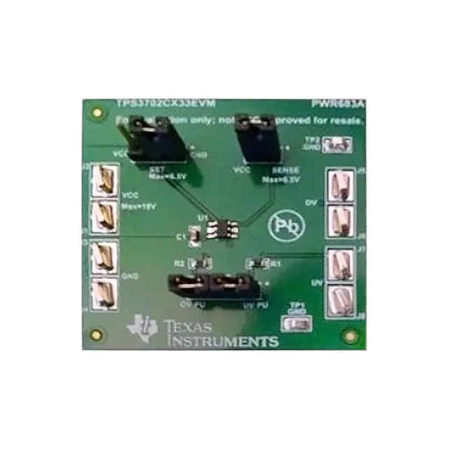
An evaluation module (EVM) is available to assist in the initial circuit performance evaluation using the TPS3702.
The TPS3702CX33EVM-683 evaluation module (and related user guide) can be requested at the Texas
Instruments website through the product folders or purchased directly from the TI eStore.
11.1.2 Device Nomenclature
Table 3 shows how to decode the function of the device based on its part number, with TPS3702CX33 used as
an example.
Table 3. Device Naming Convention
DESCRIPTION
NOMENCLATURE
VALUE
TPS3702
(high-accuracy window comparator family)
—
—
A
SET pin high = ±2%, SET pin low = ±6%
B
SET pin high = ±3%, SET pin low = ±7%
C
(nominal thresholds as a percent of the nominal
monitored voltage)
X
(hysteresis option)
33
(nominal monitored voltage option)
C
SET pin high = ±4%, SET pin low = ±9%
D
SET pin high = ±5%, SET pin low = ±10%
X
0.55%
Y
1.0%
10
1.0 V
12
1.2 V
18
1.8 V
33
3.3 V
50
5.0 V
Table 4 shows the released versions of the TPS3702, including the nominal undervoltage and overvoltage
thresholds. Contact the factory for details and availability of other options shown in Table 3; minimum order
quantities apply.
Table 4. Released Device Thresholds
20
PRODUCT
NOMINAL
SUPPLY (V)
HYSTERESI
S (%)
UV THRESHOLD
(V)
SET ≤ VIL(SET)
UV THRESHOLD
(V)
SET ≥ VIH(SET)
OV THRESHOLD
(V)
SET ≤ VIL(SET)
OV THRESHOLD
(V)
SET ≥ VIH(SET)
TPS3702CX10
1.0
0.5
0.91
0.96
1.09
1.04
TPS3702CX12
1.2
0.5
1.09
1.15
1.31
1.25
TPS3702AX18
1.8
0.5
1.69
1.76
1.91
1.84
TPS3702CX18
1.8
0.5
1.64
1.73
1.96
1.87
TPS3702AX33
3.3
0.5
3.10
3.23
3.50
3.37
TPS3702CX33
3.3
0.5
3.00
3.17
3.60
3.43
TPS3702CX50
5.0
0.5
4.55
4.80
5.45
5.20
Submit Documentation Feedback
Copyright © 2015, Texas Instruments Incorporated
Product Folder Links: TPS3702
�TPS3702
www.ti.com
SBVS251 – JANUARY 2015
11.2 Documentation Support
11.2.1 Related Documentation
Optimizing Resistor Dividers at a Comparator Input, SLVA450
TPS3702CX33EVM-683 Evaluation Module, SBVU026
11.3 Trademarks
All trademarks are the property of their respective owners.
11.4 Electrostatic Discharge Caution
This integrated circuit can be damaged by ESD. Texas Instruments recommends that all integrated circuits be handled with
appropriate precautions. Failure to observe proper handling and installation procedures can cause damage.
ESD damage can range from subtle performance degradation to complete device failure. Precision integrated circuits may be more
susceptible to damage because very small parametric changes could cause the device not to meet its published specifications.
11.5 Glossary
SLYZ022 — TI Glossary.
This glossary lists and explains terms, acronyms, and definitions.
12 Mechanical, Packaging, and Orderable Information
The following pages include mechanical, packaging, and orderable information. This information is the most
current data available for the designated devices. This data is subject to change without notice and revision of
this document. For browser-based versions of this data sheet, refer to the left-hand navigation.
Submit Documentation Feedback
Copyright © 2015, Texas Instruments Incorporated
Product Folder Links: TPS3702
21
�PACKAGE OPTION ADDENDUM
www.ti.com
10-Dec-2020
PACKAGING INFORMATION
Orderable Device
Status
(1)
Package Type Package Pins Package
Drawing
Qty
Eco Plan
(2)
Lead finish/
Ball material
MSL Peak Temp
Op Temp (°C)
Device Marking
(3)
(4/5)
(6)
TPS3702AX18DDCR
ACTIVE
SOT-23-THIN
DDC
6
3000
RoHS & Green
NIPDAU
Level-2-260C-1 YEAR
-40 to 125
ZAUO
TPS3702AX18DDCT
ACTIVE
SOT-23-THIN
DDC
6
250
RoHS & Green
NIPDAU
Level-2-260C-1 YEAR
-40 to 125
ZAUO
TPS3702AX33DDCR
ACTIVE
SOT-23-THIN
DDC
6
3000
RoHS & Green
NIPDAU
Level-2-260C-1 YEAR
-40 to 125
ZAPO
TPS3702AX33DDCT
ACTIVE
SOT-23-THIN
DDC
6
250
RoHS & Green
NIPDAU
Level-2-260C-1 YEAR
-40 to 125
ZAPO
TPS3702CX10DDCR
ACTIVE
SOT-23-THIN
DDC
6
3000
RoHS & Green
NIPDAU
Level-2-260C-1 YEAR
-40 to 125
ZARO
TPS3702CX10DDCT
ACTIVE
SOT-23-THIN
DDC
6
250
RoHS & Green
NIPDAU
Level-2-260C-1 YEAR
-40 to 125
ZARO
TPS3702CX12DDCR
ACTIVE
SOT-23-THIN
DDC
6
3000
RoHS & Green
NIPDAU
Level-2-260C-1 YEAR
-40 to 125
ZAVO
TPS3702CX12DDCT
ACTIVE
SOT-23-THIN
DDC
6
250
RoHS & Green
NIPDAU
Level-2-260C-1 YEAR
-40 to 125
ZAVO
TPS3702CX18DDCR
ACTIVE
SOT-23-THIN
DDC
6
3000
RoHS & Green
NIPDAU
Level-2-260C-1 YEAR
-40 to 125
ZAWO
TPS3702CX18DDCT
ACTIVE
SOT-23-THIN
DDC
6
250
RoHS & Green
NIPDAU
Level-2-260C-1 YEAR
-40 to 125
ZAWO
TPS3702CX33DDCR
ACTIVE
SOT-23-THIN
DDC
6
3000
RoHS & Green
NIPDAU
Level-2-260C-1 YEAR
-40 to 125
ZAQO
TPS3702CX33DDCT
ACTIVE
SOT-23-THIN
DDC
6
250
RoHS & Green
NIPDAU
Level-2-260C-1 YEAR
-40 to 125
ZAQO
TPS3702CX50DDCR
ACTIVE
SOT-23-THIN
DDC
6
3000
RoHS & Green
NIPDAU
Level-2-260C-1 YEAR
-40 to 125
ZASO
TPS3702CX50DDCT
ACTIVE
SOT-23-THIN
DDC
6
250
RoHS & Green
NIPDAU
Level-2-260C-1 YEAR
-40 to 125
ZASO
(1)
The marketing status values are defined as follows:
ACTIVE: Product device recommended for new designs.
LIFEBUY: TI has announced that the device will be discontinued, and a lifetime-buy period is in effect.
NRND: Not recommended for new designs. Device is in production to support existing customers, but TI does not recommend using this part in a new design.
PREVIEW: Device has been announced but is not in production. Samples may or may not be available.
OBSOLETE: TI has discontinued the production of the device.
(2)
RoHS: TI defines "RoHS" to mean semiconductor products that are compliant with the current EU RoHS requirements for all 10 RoHS substances, including the requirement that RoHS substance
do not exceed 0.1% by weight in homogeneous materials. Where designed to be soldered at high temperatures, "RoHS" products are suitable for use in specified lead-free processes. TI may
reference these types of products as "Pb-Free".
Addendum-Page 1
Samples
�PACKAGE OPTION ADDENDUM
www.ti.com
10-Dec-2020
RoHS Exempt: TI defines "RoHS Exempt" to mean products that contain lead but are compliant with EU RoHS pursuant to a specific EU RoHS exemption.
Green: TI defines "Green" to mean the content of Chlorine (Cl) and Bromine (Br) based flame retardants meet JS709B low halogen requirements of


 工商网监
湘ICP备2023018690号
工商网监
湘ICP备2023018690号
