User's Guide
SNVU635 – October 2018
TPS3703Q1-A4120EVM User's Guide
This user’s guide describes the operational use of the TPS3703Q1-A4120EVM evaluation module (EVM)
as a reference design for engineering demonstration and evaluation of the TPS3703-Q1, a low-power,
overvoltage and undervoltage monitor. Included in this user’s guide are setup instructions, a schematic
diagram, printed-circuit board (PCB) layout drawings, and a bill of materials for the EVM.
1
2
3
4
5
6
7
Contents
Introduction ...................................................................................................................
Hardware......................................................................................................................
2.1
EVM Connectors ....................................................................................................
2.2
Components .........................................................................................................
Operation .....................................................................................................................
3.1
Input Power (VDD)..................................................................................................
3.2
Sense .................................................................................................................
3.3
RESET ...............................................................................................................
3.4
CT ....................................................................................................................
3.5
LATCH ...............................................................................................................
3.6
Manual Reset........................................................................................................
Setup and Test ...............................................................................................................
PCB Layout ...................................................................................................................
Schematic .....................................................................................................................
Bill of Materials ...............................................................................................................
2
3
3
3
4
4
4
4
4
4
4
5
6
7
7
List of Figures
1
Top Layer Routing ........................................................................................................... 6
2
Bottom Layer Routing ....................................................................................................... 6
3
TPS3703Q1-A4120EVM Schematic
1
Test Points .................................................................................................................... 3
2
Jumpers ....................................................................................................................... 3
3
Passive Components ........................................................................................................ 3
4
Bill of Materials
......................................................................................
7
List of Tables
..............................................................................................................
7
Trademarks
All trademarks are the property of their respective owners.
SNVU635 – October 2018
Submit Documentation Feedback
TPS3703Q1-A4120EVM User's Guide
Copyright © 2018, Texas Instruments Incorporated
1
�Introduction
1
www.ti.com
Introduction
The TPS3703Q1-A4120EVM helps design engineers to evaluate the operation and performance of the
TPS3703-Q1 family of overvoltage and undervoltage monitors for possible use in their own circuit
applications. This particular EVM configuration contains the TPS3703A4120DSERQ1, an overvoltage and
undervoltage supervisor designed to monitor 1.2 V with a 4% tolerance. The family of TPS3703-Q1
provides fixed thresholds from 500 mV to 5 V and tolerance options from 3% to 7% in a small 6-pin
WSON package with an open-drain output. The TPS3703-Q1 includes a CT pin that is used to select
between two fixed reset time delays designed into each device, or an adjustable reset time delay by
connecting a capacitor to ground. A separate available SENSE input pin allows the redundancy sought by
safety-critical and high-reliability systems. Lastly, the device provides a manual reset that allows a hard
reset and a latch feature for certain desired applications.
2
TPS3703Q1-A4120EVM User's Guide
SNVU635 – October 2018
Submit Documentation Feedback
Copyright © 2018, Texas Instruments Incorporated
�Hardware
www.ti.com
2
Hardware
This section describes the connectors on the EVM, as well as how to properly connect, set up, and use
the TPS3703Q1-A4120EVM.
2.1
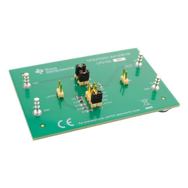
2.1.1
EVM Connectors
Test Points
Table 1 lists the test points on the EVM and their functional descriptions.
Table 1. Test Points
2.1.2
Test Point
Number
Silkscreen
Label
Function
Description
TP1
VDD
Connection to VDD pin of TPS3703Q1
Allows the user to provide voltage supply to the device
TP2
RESET
Connection to RESET pin of
TPS3703-Q1
Allows the user to measure the RESETpin
TP3
GND
Connection to ground pin of
TPS3703-Q1
Allows the user to connect to ground to provide voltage
and take measurements.
TP4
GND
Connection to ground pin of
TPS3703-Q1
Allows the user to connect to ground to provide voltage
and take measurements.
Jumpers
Table 2 lists the jumpers on the EVM and their functional descriptions.
Table 2. Jumpers
Test Point
Number
Default
Connection
J1
Closed
Reset pullup resistor to VDD
connection
Allows the user to provide onboard or external supply
voltage for the RESET pullup resistor
J2
Open
Sense pin to VDD connection
Allows the user to have monitor onboard supply
voltage or an external sense voltage
J3
2.2
2.2.1
Function
Closed, Position CT Pin to adjustable or fixed reset
7-8
delays
Description
Allows the user to evaluate fixed or adjustable reset
delays
J4
Open
Manual reset pin to GND
Allows the user to hard reset the device
J5
Open
CT Latch to VDD connection
Allows the user to reset Latch function by pulling CT
pin to VDD
Components
Passives
Table 3 lists the passive components on the EVM and their functional descriptions.
Table 3. Passive Components
Test Point
Number
Description
Value
C1
1.0 µF
Input decoupling bypass capacitor for the VDD pin
C2
0.01 µF
Bypass capacitor for sense voltage. Good for noisy applications to reduce
sensitivity to transient voltages
C3
0.033 µF
Timing capacitor for 100-ms reset delay
C4
DNP
Not populated to leave CT pin open for 10-ms reset delay. User can install
capacitor for desired reset delay.
R1
10 kΩ
Reset pullup resistor. Open-drain output requires a pullup voltage.
SNVU635 – October 2018
Submit Documentation Feedback
TPS3703Q1-A4120EVM User's Guide
Copyright © 2018, Texas Instruments Incorporated
3
�Operation
www.ti.com
Table 3. Passive Components (continued)
Test Point
Number
3
Description
Value
R2
10 kΩ
CT pullup resistor to VDD. CT pullup to VDD voltage causes 200-ms reset delay
R3
10 kΩ
CT pullup resistor to VDD. CT pullup to VDD voltage cause the latch to reset.
R4
10 kΩ
CT pulldown resistor to GND. CT pull to GND causes latch on reset.
Operation
This section describes the functionality and operation of the TPS3703Q1-A4120EVM. See the TPS3703Q1 data sheet for more information.
3.1
Input Power (VDD)
The VDD supply is connected through the TP1 test point. Apply a supply voltage to provide input power to
the device through TP1 and the common ground to test point TP3 or TP4. The supply voltage range is
between 1.7 V and 5.5 V. This device has a 6-V absolute maximum rating on the VDD pin.
3.2
Sense
The SENSE pin is the input for the monitored supply voltage rail. When the SENSE voltage goes above
the overvoltage threshold or below the undervoltage threshold, the RESET pin is driven low. If VDD is the
desired monitored voltage, install a shunt on jumper J2. If an independent voltage is being used, uninstall
the shunt on jumper J2 and apply the voltage on pin 1 of J2 where the silkscreen SENSE is labeled.
3.3
RESET
The RESET pin is an active-low, open-drain, overvoltage and undervoltage output. This pin goes low
when the SENSE voltage rises above the internally overvoltage threshold (VIT+) or below the
undervoltage threshold (VIT–). This pin is connected to a pullup resistor connected through jumper J1 to
VDD. To pull up to a desired external voltage, disconnect J1 and apply a pullup voltage to pin 2 of jumper
J1.
3.4
CT
The CT pin is for programming capacitor time delay. The CT pin offers two fixed time delays by either
connecting the CT pin to the VDD or by leaving the CT pin floating. Delay time can be programmed by
connecting an external capacitor reference to ground. The TPS3703Q1-A4120EVM provides easy access
to adjusting the reset time delay by installing a shunt on jumper J3. The provided reset delays include the
two fixed times as well as a capacitor adjusted for a 10-ms reset delay. Users can also install a capacitor
for a desired reset delay.
3.5
LATCH
The RESET pin can be latched when the CT pin is connected to GND with a pulldown resistor. Installed a
shunt on pin 1-2 on jumper J3 for the device to be in latch operation. During latch operation, when the
RESET pin is driven low, the pin will stay low regardless of the sense voltage. If the RESET is latched on
start-up, it will also stay low regardless of sense voltage. To unlatch the device, install a shunt on jumper
J5. This will provide a voltage to the CT pin that is greater than the CT pin comparator threshold voltage,
VCT. To go back into latch operation, disconnect J5 while keeping a shunt installed on pin 1-2 on J3.
3.6
Manual Reset
The manual reset pin is used to assert a reset signal in the RESET pin regardless of sense voltage. Install
a shunt on jumper J4 to connect the MR to GND. This will pull the pin lower than the MR logic low
(VMR_L) to assert a reset signal. After the MR pin is deasserted, the output goes high after the reset
delay time (tD) expires. MR can be left floating when not in use.
4
TPS3703Q1-A4120EVM User's Guide
SNVU635 – October 2018
Submit Documentation Feedback
Copyright © 2018, Texas Instruments Incorporated
�Setup and Test
www.ti.com
4
Setup and Test
This section describes a typical setup and test procedure of the TPS3703Q1-A4120EVM. For more detail
applications, see the Application Section on the TPS3703-Q1 data sheet for more information.
1.
2.
3.
4.
Set the input power supply voltage to 0 V.
Connect the ground lead from the power supply to TP3 (GND).
Connect the positive voltage lead from the power supply to TP1 (VDD).
Connect SENSE to VCC using jumper J2, or connect it to a separate power supply. For this variant of
TPS3703-Q1, an external voltage supply is required for the device to be in overvoltage and
undervoltage conditions.
5. Connect R1 to VCC using jumper J1, or connect it to a separate power supply.
6. Connect CT to the desired reset delay or latch operation using jumper J3. CT can be left open for a
10-ms reset delay.
7. Connect a voltmeter or scope across TP2 (RESET) and TP4 (GND).
8. Vary the input power-supply voltage as desired. The recommended supply voltage range is between
1.7 V and 5.5 V.
9. Vary the monitored SENSE voltage as necessary for test purposes. For this variant of TPS3703-Q1,
the supervisor is designed to monitor 1.2 V with a 4% tolerance. This means typical overvoltage and
undervoltage conditions are 1.248 V and 1.152 V respectively.
10. Connect MR to GND using jumper J4 to assert a reset signal.
11. For latch operation, pull down the CT pin by using jumper J4 pins 1-2. To unlatch the device, pull up
the CT pin by using jumper J5.
SNVU635 – October 2018
Submit Documentation Feedback
TPS3703Q1-A4120EVM User's Guide
Copyright © 2018, Texas Instruments Incorporated
5
�PCB Layout
5
www.ti.com
PCB Layout
Figure 1. Top Layer Routing
Figure 2. Bottom Layer Routing
6
TPS3703Q1-A4120EVM User's Guide
SNVU635 – October 2018
Submit Documentation Feedback
Copyright © 2018, Texas Instruments Incorporated
�Schematic
www.ti.com
6
Schematic
Figure 3. TPS3703Q1-A4120EVM Schematic
7
Bill of Materials
Table 4. Bill of Materials
Value
Size (Package
Reference)
Designator
Quantity
Description
!PCB
1
LP016
Any
C1
1
1 uF
CAP, CERM, 1 uF, 16 V, +/- 10%,
X7R, AEC-Q200 Grade 1, 0603
0603
GCM188R71C105KA64D
MuRata
C2
1
0.01 uF
CAP, CERM, 0.01 uF, 50 V, +/10%, X7R, AEC-Q200 Grade 1,
0603
0603
GCM188R71H103KA37D
MuRata
C3
1
0.033 uF
CAP, CERM, 0.033 uF, 16 V, +/10%, X7R, 0603
0603
GRM188R71C333KA01D
MuRata
H1, H2, H3,
H4
4
Bumpon, Hemisphere, 0.44 X
0.20, Clear
Transparent Bumpon
SJ-5303 (CLEAR)
3M
J1, J2, J4, J5
4
Header, 100mil, 2x1, Gold, TH
2x1 Header
TSW-102-07-G-S
Samtec
J3
1
Header, 100mil, 4x2, Gold, TH
4x2 Header
5-146256-4
TE Connectivity
R1, R2, R3,
R4
4
10.0k
RES, 10.0 k, 1%, 0.1 W, AECQ200 Grade 0, 0603
0603
CRCW060310K0FKEA
Vishay-Dale
SH-J1, SHJ2, SH-J3
3
1x2
Shunt, 100mil, Gold plated, Black
Shunt
SNT-100-BK-G
Samtec
TP1, TP2,
TP3, TP4
4
Terminal, Turret, TH, Triple
Turret
1598-2
Keystone
U1
1
Automotive High-Accuracy
Window Supervisor With Reset
Time Delay and Manual Reset
DSE0006A (WSON-6)
TPS3703A4120DSERQ1
Texas Instruments
C4
0
CAP, CERM, 0.033 uF, 16 V, +/10%, X7R, 0603
0603
GRM188R71C333KA01D
MuRata
FID1, FID2,
FID3
0
Fiducial mark. There is nothing to
buy or mount.
N/A
N/A
N/A
Printed-Circuit Board
0.033 uF
Part Number
SNVU635 – October 2018
Submit Documentation Feedback
Manufacturer
TPS3703Q1-A4120EVM User's Guide
Copyright © 2018, Texas Instruments Incorporated
7
�IMPORTANT NOTICE AND DISCLAIMER
TI PROVIDES TECHNICAL AND RELIABILITY DATA (INCLUDING DATASHEETS), DESIGN RESOURCES (INCLUDING REFERENCE
DESIGNS), APPLICATION OR OTHER DESIGN ADVICE, WEB TOOLS, SAFETY INFORMATION, AND OTHER RESOURCES “AS IS”
AND WITH ALL FAULTS, AND DISCLAIMS ALL WARRANTIES, EXPRESS AND IMPLIED, INCLUDING WITHOUT LIMITATION ANY
IMPLIED WARRANTIES OF MERCHANTABILITY, FITNESS FOR A PARTICULAR PURPOSE OR NON-INFRINGEMENT OF THIRD
PARTY INTELLECTUAL PROPERTY RIGHTS.
These resources are intended for skilled developers designing with TI products. You are solely responsible for (1) selecting the appropriate
TI products for your application, (2) designing, validating and testing your application, and (3) ensuring your application meets applicable
standards, and any other safety, security, or other requirements. These resources are subject to change without notice. TI grants you
permission to use these resources only for development of an application that uses the TI products described in the resource. Other
reproduction and display of these resources is prohibited. No license is granted to any other TI intellectual property right or to any third
party intellectual property right. TI disclaims responsibility for, and you will fully indemnify TI and its representatives against, any claims,
damages, costs, losses, and liabilities arising out of your use of these resources.
TI’s products are provided subject to TI’s Terms of Sale (www.ti.com/legal/termsofsale.html) or other applicable terms available either on
ti.com or provided in conjunction with such TI products. TI’s provision of these resources does not expand or otherwise alter TI’s applicable
warranties or warranty disclaimers for TI products.
Mailing Address: Texas Instruments, Post Office Box 655303, Dallas, Texas 75265
Copyright © 2018, Texas Instruments Incorporated
�


 工商网监
湘ICP备2023018690号
工商网监
湘ICP备2023018690号