TPS3800-xx
TPS3801-xx
TPS3802-xx
www.ti.com
SLVS219E – AUGUST 1999 – REVISED OCTOBER 2010
ULTRA-SMALL SUPPLY VOLTAGE SUPERVISORS
Check for Samples: TPS3800-xx, TPS3801-xx, TPS3802-xx
FEATURES
1
•
•
•
2
•
•
•
Small, 5-Pin SC-70 (SOT-323) Package
Supply Current of 9 mA
Power-On Reset Generator With Fixed Delay
Time
– TPS3800 = 100 ms
– TPS3801 = 200 ms
– TPS3802 = 400 ms
Precision Supply Voltage Monitor 1.8 V, 2.5 V,
2.7 V, 3 V, 3.3 V, 5 V, and Adjustable
Manual Reset Input (Except TPS3801-01)
Temperature Range: –40°C to +85°C
APPLICATIONS
•
•
•
•
•
•
•
•
Applications Using DSPs, Microcontrollers, or
Microprocessors
Wireless Communication Systems
Portable/Battery-Powered Equipment
Programmable Controls
Intelligent Instruments
Industrial Equipment
Notebook/Desktop Computers
Automotive Systems
DESCRIPTION
The TPS380x family of supervisory circuits monitor
supply voltages to provide circuit initialization and
timing supervision, primarily for DSPs and other
processor-based systems.
These devices assert a push-pull RESET signal when
the SENSE (adjustable version) or VDD (fixed version)
drops below a preset threshold. The RESET output
remains asserted for the factory programmed delay
time after the SENSE or VDD return above its
threshold.
The TPS380x devices, except the TPS3801-01,
incorporate a manual reset input (MR). A low level at
MR causes RESET to become active.
The TPS380x uses a precision reference to achieve
an overall threshold accuracy of 2%—2.5%. These
devices are available in a 5-pin SC-70 package,
which is only about half the size of a 5-pin SOT-23
package.
The TPS380x devices are fully specified over a
temperature range of –40°C to +85°C.
TPS380x . . . DCK PACKAGE
(TOP VIEW)
GND
1
5
MR
VDD = 1.8 V
100 nF
GND
2
RESET
3
TMS320VC5420
VDD
4
VDD
TPS3801E18
MR
TPS3801−01 . . . DCK PACKAGE
(TOP VIEW)
GND
1
GND
2
RESET
3
5
SENSE
4
VDD
CoreVDD
RESET
RESET
GND
GND
1
2
Please be aware that an important notice concerning availability, standard warranty, and use in critical applications of Texas
Instruments semiconductor products and disclaimers thereto appears at the end of this data sheet.
All trademarks are the property of their respective owners.
PRODUCTION DATA information is current as of publication date.
Products conform to specifications per the terms of the Texas
Instruments standard warranty. Production processing does not
necessarily include testing of all parameters.
Copyright © 1999–2010, Texas Instruments Incorporated
�TPS3800-xx
TPS3801-xx
TPS3802-xx
SLVS219E – AUGUST 1999 – REVISED OCTOBER 2010
www.ti.com
These devices have limited built-in ESD protection. The leads should be shorted together or the device placed in conductive foam
during storage or handling to prevent electrostatic damage to the MOS gates.
AVAILABLE OPTIONS (1)
TA
–40°C to 85°C
(1)
DEVICE NAME
THRESHOLD VOLTAGE
TYP DELAY TIME
TPS3801-01DCK
Adjustable (Vref = 1.14 V)
200 ms
MARKING
ARF
TPS3801E18DCK
1.71 V
200 ms
ARE
TPS3801J25DCK
2.25 V
200 ms
NJA
TPS3800G27DCK
2.5 V
95 ms
ARI
TPS3801L30DCK
2.64 V
200 ms
NPA
TPS3801K33DCK
2.93 V
200 ms
NWA
TPS3802L30DCK
2.64 V
380 ms
ASA
TPS3802K33DCK
2.93 V
380 ms
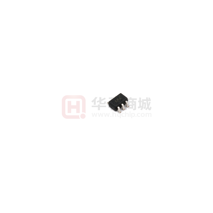
ARK
TPS3801T50DCK
4.00 V
25 ms
AVI
TPS3801I50DCK
4.55 V
200 ms
NSA
For the most current package and ordering information, see the Package Option Addendum at the end of this data sheet, or refer to our
web site at www.ti.com.
ABSOLUTE MAXIMUM RATINGS (1)
(2)
Over operating free-air temperature range (unless otherwise noted).
UNIT
Supply voltage, VDD
7V
SENSE
–0.3 V to 5 V
All other pins
–0.3 V to 7 V
MR
–0.3 V to VDD + 0.3 V
RESET
–0.3 V to VDD + 0.3 V
Maximum low-output current, IOL
5 mA
Maximum high-output current, IOH
–5 mA
Input-clamp current, IIK (VI < 0 or VI > VDD)
±20 mA
Output-clamp current, IOK (VO < 0 or VO > VDD)
Operating junction temperature range, TJ
±20 mA
(3)
–40°C to +85°C
Storage temperature range, Tstg
(1)
(2)
(3)
–65°C to +150°C
Stresses beyond those listed under absolute maximum ratings may cause permanent damage to the device. These are stress ratings
only, and functional operation of the device at these or any other conditions beyond those indicated under recommended operating
conditions is not implied. Exposure to absolute-maximum-rated conditions for extended periods may affect device reliability.
All voltage values are with respect to GND. For reliable operation, the device should not be operated at 7 V for more than t = 1000h
continuously.
Due to the low dissipation power of this device, it is assumed that TJ = TA.
RECOMMENDED OPERATING CONDITIONS
Supply voltage, VDD
MIN
MAX
TPS3801J25, TPS3801L30, TPS3801K33, TPS3801I50, TPS3801T50
2
6
All other devices
1.6
4
UNIT
V
SENSE
0
See
(1)
V
Input voltage, VI
0
VDD +0.3
V
0.7 × VDD
VDD +0.3
V
High-level input voltage, VIH
Low-level input voltage, VIL
0.3 × VDD
Input transition rise and fall rate at MR, Δt/ΔV
VPull-up
Pull-up resistor value, RESET
2
–40
V
ns/V
Ω
50µA
Operating free-air temperature range, TA
(1)
100
+85
°C
Maximum = VDD + 0.3 or 4.5 V, whichever is greater.
Submit Documentation Feedback
Copyright © 1999–2010, Texas Instruments Incorporated
Product Folder Link(s): TPS3800-xx TPS3801-xx TPS3802-xx
�TPS3800-xx
TPS3801-xx
TPS3802-xx
www.ti.com
SLVS219E – AUGUST 1999 – REVISED OCTOBER 2010
ELECTRICAL CHARACTERISTICS
Over –40°C to +85°C free-air temperature range (unless otherwise noted).
PARAMETER
TEST CONDITIONS
TPS3800-xx, TPS3801-xx,
TPS3802-xx
MIN
VOH
High-level output voltage (RESET)
VDD = 1.6 V to 6 V IOH = –500 mA
VDD –0.2
VDD = 3.3 V IOH = –2 mA
VDD –0.4
VDD = 6 V IOH = –4 mA
VOL
Low-level output voltage (RESET)
VIT–
Vhys
Negative-going input
threshold voltage (3)
Threshold hysteresis
V
0.2
VDD = 3.3 V, IOL = 2 mA
0.4
(1)
VDD ≥ 1.1 V, IOL = 50 mA
0.2
1.117
1.14
1.163
TPS380xE18
1.67
1.71
1.75
TPS380xJ25
2.2
2.25
2.3
2.45
2.5
2.55
2.58
2.64
2.7
TPS380xK33
2.87
2.93
2.99
TPS380xI50
4.45
4.55
4.65
TPS380xT50
3.92
4
4.08
TPS380xL30
TA = –40°C to 85°C
TPS380x-01
15
TPS380xx18
25
TPS380xx25
30
TPS380xx27
35
TPS380xx30
35
TPS380xx33
40
High-level input current (MR)
MR = 0.7×VDD, VDD = 6 V
IIL
Low-level input current (MR)
MR = 0 V, VDD = 6 V
II
Input current (SENSE)
Supply current
TPS3801E18,
TPS3800G27,
TPS3802K33,
TPS3802L30
Ci
(1)
(2)
(3)
Input capacitance
V
mV
–40
–60
–100
–130
–200
–340
–25
TPS3801-01
V
60
IIH
TPS3801J25,
TPS3801L30,
TPS3801K33,
TPS3801I50,
TPS3801T50
V
0.4
TPS380x-01
TPS380xG27
UNIT
VDD –0.4
TPS380xx50
IDD
MAX
VDD = 1.6 V to 6 V, IOL = 500 mA
VDD = 6 V, IOL = 4 mA
Power-up reset voltage (2)
(1)
TYP
mA
25
VDD = 2 V, MR and output
unconnected
9
12
VDD = 6 V, MR and output
unconnected
20
25
VDD = 1.6 V, SENSE = 0 V to VDD,
output unconnected
7
10
VDD = 4 V, SENSE = 0 V to VDD,
output unconnected
9
12
VDD = 1.6 V, MR and output
unconnected
8
11
13
18
nA
mA
VDD = 4 V, MR and output
unconnected
VI = 0 V to VDD
5
pF
Only valid for the TPS3801J25, TPS3801L30, TPS3801K33, TPS3801I50, and TPS3801T50.
The lowest supply voltage at which RESET becomes active. tr, VDD ≥ 15 ms/V.
To ensure the best stability of the threshold voltage, a bypass capacitor (0.1-mF ceramic) should be placed near the supply terminals.
Copyright © 1999–2010, Texas Instruments Incorporated
Submit Documentation Feedback
Product Folder Link(s): TPS3800-xx TPS3801-xx TPS3802-xx
3
�TPS3800-xx
TPS3801-xx
TPS3802-xx
SLVS219E – AUGUST 1999 – REVISED OCTOBER 2010
www.ti.com
TIMING REQUIREMENTS
at RL = 1 MΩ, CL = 50 pF, TA = +25°C
PARAMETER
TEST CONDITIONS
at SENSE
tw
Pulse width
MIN
TYP
VDD = 1.6 V, VIH = 1.1 × VIT–, VIL = 0.9 × VIT–
1
at VDD
VDD = VIT– + 0.2 V, VDD = VIT– –0.2 V
3
at MR
VDD ≥ VIT– + 0.2 V, VIL = 0.3 × VDD, VIH = 0.7 × VDD
MAX
UNIT
ms
100
ns
SWITCHING CHARACTERISTICS
at RL = 1 MΩ, CL = 50 pF, TA = +25°C
PARAMETER
TEST CONDITIONS
MIN
TPS3801T50
td
VDD ≥ VIT– + 0.2 V,
MR ≥ 0.7 × VDD
See timing diagram
TPS3800
RESET recovery delay time
TPS3801
TPS3802
MR to RESET delay
tPHL
Propagation (delay) time, high-to-low-level
output
TYP
15
VDD to RESET delay
SENSE to RESET
MAX
25
35
60
95
140
120
200
280
240
380
560
VDD ≥ VIT– + 0.2 V,
VIL = 0.3 × VDD,
VIH = 0.7 × VDD
VIL = VIT– – 0.2 V,
VIH = VIT– + 0.2 V
UNIT
ms
15
ns
1
ms
TIMING DIAGRAM
VDD
V(NOM)
VIT
1.1 V
t
MR
1
ÎÎ
ÎÎ
ÎÎ
ÎÎ
ÎÎ
ÎÎ
ÎÎ
ÎÎ
ÎÎ
ÎÎ
ÎÎ
ÎÎ
0
RESET
1
0
td
td
t
t
td
Undefined Behavior of
RESET Output For VDD < 1.1 V
NOTE: RESET should not be forced high during the power-up sequence (until VDD > 1.1 V).
4
Submit Documentation Feedback
Copyright © 1999–2010, Texas Instruments Incorporated
Product Folder Link(s): TPS3800-xx TPS3801-xx TPS3802-xx
�TPS3800-xx
TPS3801-xx
TPS3802-xx
www.ti.com
SLVS219E – AUGUST 1999 – REVISED OCTOBER 2010
FUNCTIONAL BLOCK DIAGRAMS
FUNCTION/TRUTH TABLE, TPS380x
RESET
VDD>VIT
MR
L
0
L
L
1
L
H
0
L
H
1
H
TPS380x
VDD
MR
Reset
Logic
+
Timer
30 kΩ
R1
_
VDD
RESET
+
R2
GND
Oscillator
Reference
Voltage
of 1.14 V
Figure 1.
TPS3801−01
VDD
Device Supply
Voltage
VDD
Reset
Logic
+
Timer
_
SENSE
RESET
+
Oscillator
Reference
Voltage
of 1.14 V
Figure 2.
Copyright © 1999–2010, Texas Instruments Incorporated
Submit Documentation Feedback
Product Folder Link(s): TPS3800-xx TPS3801-xx TPS3802-xx
5
�TPS3800-xx
TPS3801-xx
TPS3802-xx
SLVS219E – AUGUST 1999 – REVISED OCTOBER 2010
www.ti.com
TYPICAL CHARACTERISTICS
spacer
LOW-LEVEL OUTPUT VOLTAGE
vs
LOW-LEVEL OUTPUT CURRENT
SUPPLY CURRENT
vs
SUPPLY VOLTAGE
50
2.75
VDD = 2.5 V
MR = OPEN
MR = OPEN
TA = 25°C
40
2.25
30
2.00
TA = 25°C
1.75
1.50
TA = 85°C
1.25
TA = 0°C
1.00
0.75
TA = -40°C
0.50
I DD − Supply Current − µ A
VOL − Low-Level Output Voltage − V
2.50
20
10
TPS3801J25
0
−10
−20
−30
−40
0.25
0.00
0.0
−50
2.5
5.0
7.5
10.0
−2
12.5
0
Figure 4.
HIGH-LEVEL OUTPUT VOLTAGE
vs
HIGH-LEVEL OUTPUT CURRENT
HIGH-LEVEL OUTPUT VOLTAGE
vs
HIGH-LEVEL OUTPUT CURRENT
6
3.00
VDD = 6.0 V
MR = OPEN
5.5
5.0
4.5
TA = -40°C
4.0
3.5
TA = 0°C
3.0
2.5
TA = 85°C
2.0
1.5
1.0
VDD = 2.5 V
MR = OPEN
2.75
TA = 25°C
VOH − High-Level Output Voltage − V
6.0
VOH − High-Level Output Voltage − V
4
Figure 3.
6.5
2.50
2.25
2.00
TA = -40°C
1.75
1.50
TA = 0°C
1.25
1.00
TA = 85°C
0.75
0.50
TA = 25°C
0.25
0.5
0.00
0.0
0
−10
−20
−30
−40
IOH − High-Level Output Current − mA
−50
0
−2
Submit Documentation Feedback
−4
−6
−8
−10
IOH − High-Level Output Current − mA
Figure 5.
6
2
VDD − Supply Voltage − V
IOL − Low-Level Output Current − mA
Figure 6.
Copyright © 1999–2010, Texas Instruments Incorporated
Product Folder Link(s): TPS3800-xx TPS3801-xx TPS3802-xx
�TPS3800-xx
TPS3801-xx
TPS3802-xx
www.ti.com
SLVS219E – AUGUST 1999 – REVISED OCTOBER 2010
TYPICAL CHARACTERISTICS (continued)
spacer
INPUT CURRENT
vs
INPUT VOLTAGE AT MR
spacer
MINIMUM PULSE DURATION AT VDD
vs
VDD THRESHOLD OVERDRIVE VOLTAGE
3.5
100
VDD = 6 V
TA = 25°C
tw − Minimum Pulse Duration at VDD − µs
I − Input Current − µ A
I
0
MR = OPEN
−100
−200
−300
−400
−500
−2
3
2.5
2
1.5
1
0.5
0
0
2
4
0
6
0.4
0.6
0.8
Figure 7.
Figure 8.
NORMALIZED INPUT THRESHOLD VOLTAGE
vs
FREE-AIR TEMPERATURE AT VDD
NORMALIZED INPUT THRESHOLD VOLTAGE
vs
FREE-AIR TEMPERATURE AT VDD
MR = OPEN
1.000
0.999
0.998
0.997
TPS3801S25
TPS3801L30
TPS3801K33
TPS3801I50
TPS3801T50
0.996
0.995
−40
1
1.006
1.001
VIT − Normalized Input Threshold Voltage − V
VIT (TA)/ VIT (25 °C )
VI − Input Voltage at MR − V
Normalized Input Threshold Voltage
0.2
VDD Threshold Overdrive Voltage − V
1.002
1
0.998
0.996
0.994
0.992
0.990
0.988
−40
−20
0
20
40
60
TA − Free-Air Temperature at VDD − °C
85
TPS3801−01
TPS3801E18
TPS3800
TPS3802
1.004
−20
0
Figure 9.
Copyright © 1999–2010, Texas Instruments Incorporated
20
40
60
80
TA − Free-Air Temperature at VDD − °C
Figure 10.
Submit Documentation Feedback
Product Folder Link(s): TPS3800-xx TPS3801-xx TPS3802-xx
7
�TPS3800-xx
TPS3801-xx
TPS3802-xx
SLVS219E – AUGUST 1999 – REVISED OCTOBER 2010
www.ti.com
Changes from Revision D (December 2006) to Revision E
•
8
Page
Added Pull-up resistor value, RESET to the Recommended Operating Conditions Table .................................................. 2
Submit Documentation Feedback
Copyright © 1999–2010, Texas Instruments Incorporated
Product Folder Link(s): TPS3800-xx TPS3801-xx TPS3802-xx
�PACKAGE OPTION ADDENDUM
www.ti.com
14-Oct-2022
PACKAGING INFORMATION
Orderable Device
Status
(1)
Package Type Package Pins Package
Drawing
Qty
Eco Plan
(2)
Lead finish/
Ball material
MSL Peak Temp
Op Temp (°C)
Device Marking
(3)
Samples
(4/5)
(6)
HPA00763DCKR
ACTIVE
SC70
DCK
5
3000
TBD
Call TI
Call TI
-40 to 85
TPS3800G27DCKR
ACTIVE
SC70
DCK
5
3000
RoHS & Green
NIPDAU
Level-1-260C-UNLIM
-40 to 85
ARI
Samples
TPS3801-01DCKR
ACTIVE
SC70
DCK
5
3000
RoHS & Green
NIPDAU
Level-1-260C-UNLIM
-40 to 85
ARF
Samples
TPS3801-01DCKRG4
ACTIVE
SC70
DCK
5
3000
RoHS & Green
NIPDAU
Level-1-260C-UNLIM
-40 to 85
ARF
Samples
TPS3801E18DCKR
ACTIVE
SC70
DCK
5
3000
RoHS & Green
NIPDAU
Level-1-260C-UNLIM
-40 to 85
ARE
Samples
TPS3801I50DCKR
ACTIVE
SC70
DCK
5
3000
RoHS & Green
NIPDAU
Level-1-260C-UNLIM
-40 to 85
NSA
Samples
TPS3801I50DCKRG4
ACTIVE
SC70
DCK
5
3000
RoHS & Green
NIPDAU
Level-1-260C-UNLIM
-40 to 85
NSA
Samples
TPS3801J25DCKR
ACTIVE
SC70
DCK
5
3000
RoHS & Green
NIPDAU
Level-1-260C-UNLIM
-40 to 85
NJA
Samples
TPS3801K33DCKR
ACTIVE
SC70
DCK
5
3000
RoHS & Green
NIPDAU
Level-1-260C-UNLIM
-40 to 85
NWA
Samples
TPS3801K33DCKRG4
ACTIVE
SC70
DCK
5
3000
RoHS & Green
NIPDAU
Level-1-260C-UNLIM
-40 to 85
NWA
Samples
TPS3801L30DCKR
ACTIVE
SC70
DCK
5
3000
RoHS & Green
NIPDAU
Level-1-260C-UNLIM
-40 to 85
NPA
Samples
TPS3801T50DCKR
ACTIVE
SC70
DCK
5
3000
RoHS & Green
NIPDAU
Level-1-260C-UNLIM
-40 to 85
AVI
Samples
TPS3802K33DCKR
ACTIVE
SC70
DCK
5
3000
RoHS & Green
NIPDAU
Level-1-260C-UNLIM
-40 to 85
ARK
Samples
TPS3802L30DCKR
ACTIVE
SC70
DCK
5
3000
RoHS & Green
NIPDAU
Level-1-260C-UNLIM
-40 to 85
ASA
Samples
Samples
(1)
The marketing status values are defined as follows:
ACTIVE: Product device recommended for new designs.
LIFEBUY: TI has announced that the device will be discontinued, and a lifetime-buy period is in effect.
NRND: Not recommended for new designs. Device is in production to support existing customers, but TI does not recommend using this part in a new design.
PREVIEW: Device has been announced but is not in production. Samples may or may not be available.
OBSOLETE: TI has discontinued the production of the device.
(2)
RoHS: TI defines "RoHS" to mean semiconductor products that are compliant with the current EU RoHS requirements for all 10 RoHS substances, including the requirement that RoHS substance
do not exceed 0.1% by weight in homogeneous materials. Where designed to be soldered at high temperatures, "RoHS" products are suitable for use in specified lead-free processes. TI may
reference these types of products as "Pb-Free".
Addendum-Page 1
�PACKAGE OPTION ADDENDUM
www.ti.com
14-Oct-2022
RoHS Exempt: TI defines "RoHS Exempt" to mean products that contain lead but are compliant with EU RoHS pursuant to a specific EU RoHS exemption.
Green: TI defines "Green" to mean the content of Chlorine (Cl) and Bromine (Br) based flame retardants meet JS709B low halogen requirements of


 工商网监
湘ICP备2023018690号
工商网监
湘ICP备2023018690号

