TPS3809J25, TPS3809L30
TPS3809K33, TPS3809I50
www.ti.com
SLVS228C – AUGUST 1999 – REVISED OCTOBER 2013
3-Pin Supply Voltage Supervisors
Check for Samples: TPS3809J25, TPS3809L30, TPS3809K33, TPS3809I50
FEATURES
DESCRIPTION
•
•
•
The TPS3809 family of supervisory circuits provides
circuit initialization and timing supervision, primarily
for DSPs and processor-based systems.
1
2
•
•
3-Pin SOT-23 Package
Supply Current of 9 μA (Typical)
Precision Supply Voltage Monitor
2.5 V, 3 V, 3.3 V, 5 V
Pin-For-Pin Compatible With MAX 809
Temperature Range: –40°C to +85°C
APPLICATIONS
•
•
•
•
•
•
•
•
Applications Using DSPs, Microcontrollers, or
Microprocessors
Wireless Communication Systems
Portable/Battery-Powered Equipment
Programmable Controls
Intelligent Instruments
Industrial Equipment
Notebook/Desktop Computers
Automotive Systems
DBV PACKAGE
TOP VIEW)
GND
During power-on, RESET is asserted when the
supply voltage VDD becomes higher than 1.1 V.
Thereafter, the supervisory circuit monitors VDD and
keeps RESET active as long as VDD remains below
the threshold voltage VIT. An internal timer delays the
return of the output to the inactive state (high) to
ensure proper system reset. The delay time, td(typ) =
200 ms, starts after VDD has risen above the
threshold voltage VIT. When the supply voltage drops
below the threshold voltage VIT, the output becomes
active (low) again. No external components are
required. All the devices of this family have a fixed
sense-threshold voltage VIT set by an internal voltage
divider.
The product spectrum is designed for supply voltages
of 2.5 V, 3 V, 3.3 V, and 5 V. The circuits are
available in a 3-pin SOT-23. The TPS3809 devices
are characterized for operation over a temperature
range of –40°C to 85°C.
TYPICAL APPLICATION
1
TPS76333
3.3 V
3
VDD
5V
IN
OUT
GND
RESET
VDD
2
VDD
TMS320LC54x
TPS3809K33
RESET
RESET
GND
GND
1
2
Please be aware that an important notice concerning availability, standard warranty, and use in critical applications of
Texas Instruments semiconductor products and disclaimers thereto appears at the end of this data sheet.
All trademarks are the property of their respective owners.
PRODUCTION DATA information is current as of publication date.
Products conform to specifications per the terms of the Texas
Instruments standard warranty. Production processing does not
necessarily include testing of all parameters.
Copyright © 1999–2013, Texas Instruments Incorporated
�TPS3809J25, TPS3809L30
TPS3809K33, TPS3809I50
SLVS228C – AUGUST 1999 – REVISED OCTOBER 2013
www.ti.com
These devices have limited built-in ESD protection. The leads should be shorted together or the device placed in conductive foam
during storage or handling to prevent electrostatic damage to the MOS gates.
AVAILABLE OPTIONS (1)
TA
DEVICE NAME
–40°C to 85°C
(1)
THRESHOLD VOLTAGE
MARKING
TPS3809J25DBVR
TPS3809J25DBVT
2.25 V
PCZI
TPS3809L30DBVR
TPS3809L30DBVT
2.64 V
PDAI
TPS3809K33DBVR
TPS3809K33DBVT
2.93 V
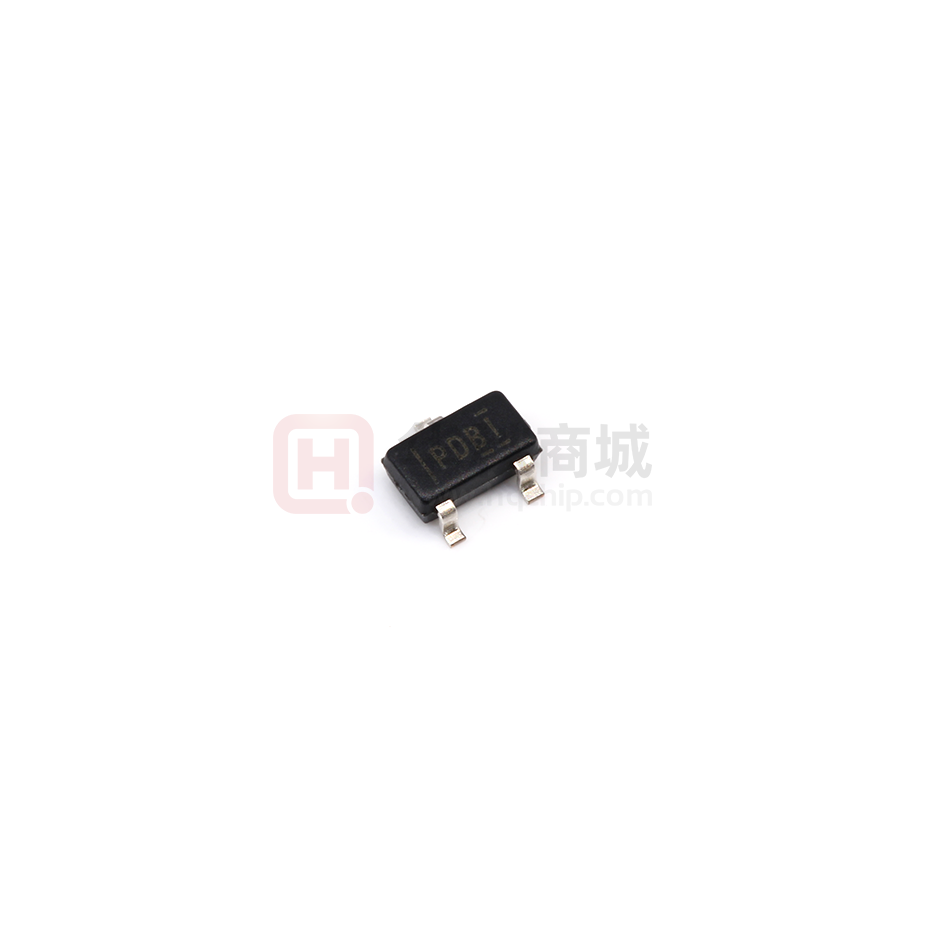
PDBI
TPS3809I50DBVR
TPS3809I50DBVT
4.55 V
PDCI
For the most current package and ordering information, see the Package Option Addendum at the end of this data sheet, or visit the
device product folder at www.ti.com.
ORDERING INFORMATION
FUNCTION/TRUTH TABLE, TPS3809
VDD>VIT
RESET
0
L
1
H
TPS380
9
J
25 DBV R
Reel
Package
Nominal Supply Voltage
Nominal Threshold Voltage
Functionality
Family
ABSOLUTE MAXIMUM RATINGS (1) (2)
Over operating free-air temperature range (unless otherwise noted).
UNIT
Supply voltage, VDD
7V
All other pins
–0.3 V to 7 V
Maximum low-output current, IOL
5 mA
Maximum high-output current, IOH
–5 mA
Input-clamp current, IIK (VI < 0 or VI > VDD)
±20 mA
Output-clamp current, IOK (VO < 0 or VO > VDD)
±20 mA
Continuous total power dissipation
See Dissipation Rating Table
Operating free-air temperature range, TA
–40°C to 85°C
Storage temperature range, Tstg
–65°C to 150°C
(1)
(2)
Stresses beyond those listed under absolute maximum ratings may cause permanent damage to the device. These are stress ratings
only, and functional operation of the device at these or any other conditions beyond those indicated under recommended operating
conditions is not implied. Exposure to absolute-maximum-rated conditions for extended periods may affect device reliability.
All voltage values are with respect to GND. For reliable operation, the device should not be operated at 7 V for more than t = 1000h
continuously.
DISSIPATION RATINGS
PACKAGE
TA < 25°C
POWER RATING
DERATING FACTOR
ABOVE TA < 25°C
TA = 70°C
POWER RATING
TA = 85°C
POWER RATING
DBV
437 mW
3.5 mW/°C
280 mW
227 mW
RECOMMENDED OPERATING CONDITIONS
Supply voltage, VDD
MIN
MAX
2
6
V
50
µA
+85
°C
RESET current sink during startup
Operating free-air temperature range, TA
2
Submit Documentation Feedback
–40
UNIT
Copyright © 1999–2013, Texas Instruments Incorporated
Product Folder Links: TPS3809J25 TPS3809L30 TPS3809K33 TPS3809I50
�TPS3809J25, TPS3809L30
TPS3809K33, TPS3809I50
www.ti.com
SLVS228C – AUGUST 1999 – REVISED OCTOBER 2013
ELECTRICAL CHARACTERISTICS
Over recommended operating free-air temperature range (unless otherwise noted).
PARAMETER
TPS3800-xx, TPS3801-xx, TPS3802xx
TEST CONDITIONS
MIN
VOH
VOL
High-level output voltage
Low-level output voltage
Power-up reset voltage (1)
VDD = 2.5 V to 6 V IOH = –500 μA
VDD –0.2
VDD = 3.3 V IOH = –2 mA
VDD –0.4
VDD = 6 V IOH = –4 mA
VDD –0.4
Negative-going input
threshold voltage (2)
TPS3809L30
TPS3809K33
Threshold hysteresis
IDD
Supply current
Ci
Input capacitance
(1)
(2)
UNIT
V
0.2
VDD = 3.3 V, IOL = 2 mA
0.4
VDD = 6 V, IOL = 4 mA
0.4
VDD ≥ 1.1 V, IOL = 50 μA
V
0.2
TA = –40°C to 85°C
TPS3809I50
Vhys
MAX
VDD = 2 V to 6 V, IOL = 500 μA
TPS3809J25
VIT–
TYP
2.2
2.25
2.3
2.58
2.64
2.7
2.87
2.93
2.99
4.45
4.55
4.65
TPS3809J25
30
TPS3809L30
35
TPS3809K33
40
TPS3809I50
60
V
mV
VDD = 2 V, output unconnected
9
12
VDD = 6 V, output unconnected
20
25
VI = 0 V to VDD
V
μA
5
pF
The lowest supply voltage at which RESET becomes active. tr, VDD ≥ 15 μs/V.
To ensure the best stability of the threshold voltage, a bypass capacitor (0.1-μF ceramic) should be placed near the supply terminals.
TIMING REQUIREMENTS
at RL = 1 MΩ, CL = 50 pF, TA = 25°C
PARAMETER
tw
Pulse width
TEST CONDITIONS
at VDD
MIN
VDD = VIT– + 0.2 V, VDD = VIT– –0.2 V
TYP
MAX
UNIT
μs
3
SWITCHING CHARACTERISTICS
at RL = 1 MΩ, CL = 50 pF, TA = 25°C
PARAMETER
TEST CONDITIONS
td
Delay time
VDD ≥ VIT– + 0.2 V,
See timing diagram
tPHL
Propagation (delay) time, high-to-low-level
output
Copyright © 1999–2013, Texas Instruments Incorporated
VDD to RESET delay
MIN
VIL = VIT– – 0.2 V,
VIH = VIT– + 0.2 V
120
TYP
MAX
200
280
1
Submit Documentation Feedback
Product Folder Links: TPS3809J25 TPS3809L30 TPS3809K33 TPS3809I50
UNIT
ms
μs
3
�TPS3809J25, TPS3809L30
TPS3809K33, TPS3809I50
SLVS228C – AUGUST 1999 – REVISED OCTOBER 2013
www.ti.com
TIMING DIAGRAM
VDD
V(NOM)
VIT
1.1 V
t
RESET
aaaaa
aaaaa
aaaaa
aaaaa
aaaaa
1
aaaa
aaaa
aaaa
aaaa
aaaa
0
td
t
td
For VDD< 1.1 V Undefined
Behavior of RESET Output
FUNCTIONAL BLOCK DIAGRAM
TPS3809
R1
_
VDD
+
Reset
Logic
+
Timer
RESET
R2
GND
Oscillator
Reference
Voltage
of 1.137 V
4
Submit Documentation Feedback
Copyright © 1999–2013, Texas Instruments Incorporated
Product Folder Links: TPS3809J25 TPS3809L30 TPS3809K33 TPS3809I50
�TPS3809J25, TPS3809L30
TPS3809K33, TPS3809I50
www.ti.com
SLVS228C – AUGUST 1999 – REVISED OCTOBER 2013
TYPICAL CHARACTERISTICS
spacer
LOW-LEVEL OUTPUT VOLTAGE
vs
LOW-LEVEL OUTPUT CURRENT
50
2.75
VDD = 2.5 V
o
2.50
40
2.25
30
2.00
o
TA = 25 C
1.75
1.50
o
TA = 85 C
1.25
o
TA = 0 C
1.00
0.75
o
TA = –40 C
0.50
IDD – Supply Current – mA
VOL – Low-Level Output Voltage – V
SUPPLY CURRENT
vs
SUPPLY VOLTAGE
TA = 25 C
20
10
TPS3809J25
0
–10
–20
–30
–40
0.25
–50
0
0
2.5
5.0
7.5
10.0
–2
12.5
IOL – Low-Level Output Current – mA
Figure 1.
HIGH-LEVEL OUTPUT VOLTAGE
vs
HIGH-LEVEL OUTPUT CURRENT
6.5
5.0
o
TA = –40 C
4.0
3.5
o
TA = 0 C
3.0
o
2.5
TA = 85 C
2.0
1.5
1.0
VDD = 2.5 V
2.75
o
TA = 25 C
VOH – High-Level Output Voltage – V
VOH – High-Level Output Voltage – V
3.00
5.5
4.5
6
HIGH-LEVEL OUTPUT VOLTAGE
vs
HIGH-LEVEL OUTPUT CURRENT
VDD = 6 V
6.0
0
2
4
VDD – Supply Voltage – V
Figure 2.
2.50
2.25
2.00
o
TA = –40 C
1.75
1.50
o
TA = 0 C
1.25
1.00
o
TA = 85 C
0.75
o
0.50
TA = 25 C
0.25
0.5
0
0
0
–10
–20
–30
–40
IOH – High-Level Output Current – mA
Figure 3.
Copyright © 1999–2013, Texas Instruments Incorporated
–50
0
–2
–4
–6
–8
IOH – High-Level Output Current – mA
Figure 4.
Submit Documentation Feedback
Product Folder Links: TPS3809J25 TPS3809L30 TPS3809K33 TPS3809I50
–10
5
�TPS3809J25, TPS3809L30
TPS3809K33, TPS3809I50
SLVS228C – AUGUST 1999 – REVISED OCTOBER 2013
www.ti.com
TYPICAL CHARACTERISTICS (continued)
SPACE
NORMALIZED INPUT THRESHOLD VOLTAGE
vs
FREE-AIR TEMPERATURE AT VDD
3.5
1.001
VDD = 2.3 V
t w – Minimum Pulse Duration at VDD – ms
Normalized Threshold Voltage VIT (TA), VIT (25oC)
SPACE
NORMALIZED INPUT THRESHOLD VOLTAGE
vs
FREE-AIR TEMPERATURE AT VDD
1.000
0.999
0.998
0.997
0.996
0.995
–40
3.0
2.5
2.0
1.5
1.0
0.5
0
–20
0
20
40
60
o
TA – Free-Air Temperature – C
Figure 5.
85
0
0.2
0.4
0.6
0.8
1.0
VDD – Threshold Overdrive Voltage – V
Figure 6.
REVISION HISTORY
NOTE: Page numbers for previous revisions may differ from page numbers in the current version.
Changes from Revision B (July 2012) to Revision C
Page
•
Changed front page and page flow to match current standard look and feel ....................................................................... 1
•
Changed "Operating junction temperature range" to "Operating free-air temperature range" in Absolute Maximum
Ratings (typo) ........................................................................................................................................................................ 2
Changes from Revision A (October 2010) to Revision B
•
Page
Changed the Pull-up resistor value, RESET To: RESET current sink during startup in the Recommended Operating
Conditions Table ................................................................................................................................................................... 2
Changes from Original (August 1999) to Revision A
•
6
Page
Added Pull-up resistor value, RESET to the Recommended Operating Conditions Table .................................................. 2
Submit Documentation Feedback
Copyright © 1999–2013, Texas Instruments Incorporated
Product Folder Links: TPS3809J25 TPS3809L30 TPS3809K33 TPS3809I50
�PACKAGE OPTION ADDENDUM
www.ti.com
24-Aug-2018
PACKAGING INFORMATION
Orderable Device
Status
(1)
Package Type Package Pins Package
Drawing
Qty
Eco Plan
Lead/Ball Finish
MSL Peak Temp
(2)
(6)
(3)
Op Temp (°C)
Device Marking
(4/5)
TPS3809I50DBVR
ACTIVE
SOT-23
DBV
3
3000
Green (RoHS
& no Sb/Br)
CU NIPDAU | Call TI
Level-1-260C-UNLIM
-40 to 85
PDCI
TPS3809I50DBVRG4
ACTIVE
SOT-23
DBV
3
3000
Green (RoHS
& no Sb/Br)
CU NIPDAU
Level-1-260C-UNLIM
-40 to 85
PDCI
TPS3809I50DBVT
ACTIVE
SOT-23
DBV
3
250
Green (RoHS
& no Sb/Br)
CU NIPDAU | Call TI
Level-1-260C-UNLIM
-40 to 85
PDCI
TPS3809J25DBVR
ACTIVE
SOT-23
DBV
3
3000
Green (RoHS
& no Sb/Br)
CU NIPDAU
Level-1-260C-UNLIM
-40 to 85
PCZI
TPS3809J25DBVT
ACTIVE
SOT-23
DBV
3
250
Green (RoHS
& no Sb/Br)
CU NIPDAU
Level-1-260C-UNLIM
-40 to 85
PCZI
TPS3809J25DBVTG4
ACTIVE
SOT-23
DBV
3
250
Green (RoHS
& no Sb/Br)
CU NIPDAU
Level-1-260C-UNLIM
-40 to 85
PCZI
TPS3809K33DBVR
ACTIVE
SOT-23
DBV
3
3000
Green (RoHS
& no Sb/Br)
CU NIPDAU
Level-1-260C-UNLIM
-40 to 85
PDBI
TPS3809K33DBVRG4
ACTIVE
SOT-23
DBV
3
3000
Green (RoHS
& no Sb/Br)
CU NIPDAU
Level-1-260C-UNLIM
-40 to 85
PDBI
TPS3809K33DBVT
ACTIVE
SOT-23
DBV
3
250
Green (RoHS
& no Sb/Br)
CU NIPDAU
Level-1-260C-UNLIM
-40 to 85
PDBI
TPS3809K33DBVTG4
ACTIVE
SOT-23
DBV
3
250
Green (RoHS
& no Sb/Br)
CU NIPDAU
Level-1-260C-UNLIM
-40 to 85
PDBI
TPS3809L30DBVR
ACTIVE
SOT-23
DBV
3
3000
Green (RoHS
& no Sb/Br)
CU NIPDAU
Level-1-260C-UNLIM
-40 to 85
PDAI
TPS3809L30DBVRG4
ACTIVE
SOT-23
DBV
3
3000
Green (RoHS
& no Sb/Br)
CU NIPDAU
Level-1-260C-UNLIM
-40 to 85
PDAI
TPS3809L30DBVT
ACTIVE
SOT-23
DBV
3
250
Green (RoHS
& no Sb/Br)
CU NIPDAU
Level-1-260C-UNLIM
-40 to 85
PDAI
TPS3809L30DBVTG4
ACTIVE
SOT-23
DBV
3
250
Green (RoHS
& no Sb/Br)
CU NIPDAU
Level-1-260C-UNLIM
-40 to 85
PDAI
(1)
The marketing status values are defined as follows:
ACTIVE: Product device recommended for new designs.
LIFEBUY: TI has announced that the device will be discontinued, and a lifetime-buy period is in effect.
NRND: Not recommended for new designs. Device is in production to support existing customers, but TI does not recommend using this part in a new design.
PREVIEW: Device has been announced but is not in production. Samples may or may not be available.
OBSOLETE: TI has discontinued the production of the device.
Addendum-Page 1
Samples
�PACKAGE OPTION ADDENDUM
www.ti.com
24-Aug-2018
(2)
RoHS: TI defines "RoHS" to mean semiconductor products that are compliant with the current EU RoHS requirements for all 10 RoHS substances, including the requirement that RoHS substance
do not exceed 0.1% by weight in homogeneous materials. Where designed to be soldered at high temperatures, "RoHS" products are suitable for use in specified lead-free processes. TI may
reference these types of products as "Pb-Free".
RoHS Exempt: TI defines "RoHS Exempt" to mean products that contain lead but are compliant with EU RoHS pursuant to a specific EU RoHS exemption.
Green: TI defines "Green" to mean the content of Chlorine (Cl) and Bromine (Br) based flame retardants meet JS709B low halogen requirements of