TPS3818
www.ti.com ......................................................................................................................................................... SBVS106A – MAY 2008 – REVISED AUGUST 2008
Low Quiescent Current, Accurate Programmable-Delay
Supervisory Circuit
FEATURES
DESCRIPTION
1
• Power-On Reset Generator with Adjustable
Delay Time: 1.25ms to 10s
• Very Low Quiescent Current: 2.4µA typ
• High Threshold Accuracy: 0.5% typ
• Fixed Threshold Voltages for Standard Voltage
Rails from 0.9V to 5V and Adjustable Voltage
Down to 0.4V Are Available
• Manual Reset (MR) Input
• Open-Drain RESET Output
• Temperature Range: –40°C to +125°C
• Small SOT23 and 2mm × 2mm QFN Packages
The
TPS3818xxx
family
of
microprocessor
supervisory circuits monitor system voltages from
0.4V to 5.0V, asserting an open-drain RESET signal
when the SENSE voltage drops below a preset
threshold or when the manual reset (MR) pin drops to
a logic low. The RESET output remains low for the
user-adjustable delay time after the SENSE voltage
and manual reset (MR) return above the respective
thresholds.
23
The TPS3818 uses a precision reference to achieve
0.5% threshold accuracy for VIT ≤ 3.3V. The reset
delay time can be set to 20ms by disconnecting the
CT pin, 300ms by connecting the CT pin to VDD using
a resistor, or can be user-adjusted between 1.25ms
and 10s by connecting the CT pin to an external
capacitor. When used with an external capacitor, the
TPS3818xxx gives a more accurate delay time than
the similar TPS3808xxx device. The TPS3818 has a
very low typical quiescent current of 2.4µA so it is
well-suited to battery-powered applications. It is
available in either a small SOT23 and an ultra-small
2mm × 2mm QFN PowerPAD™ package, and is fully
specified over a temperature range of –40°C to
+125°C (TJ).
APPLICATIONS
•
•
•
•
•
DSP or Microcontroller Applications
Notebook/Desktop Computers
PDAs/Hand-Held Products
Portable/Battery-Powered Products
FPGA/ASIC Applications
1.2V
3.3V
DBV PACKAGE
SOT23
(TOP VIEW)
SENSE VDD
SENSE VDD
TPS3818G12
TPS3818G33
RESET
CT
GND
MR
CT
RESET
GND
Typical Application Circuit
VI/O
VCORE
RESET
1
6
VDD
GND
2
5
SENSE
MR
3
4
CT
DSP
GPIO
GND
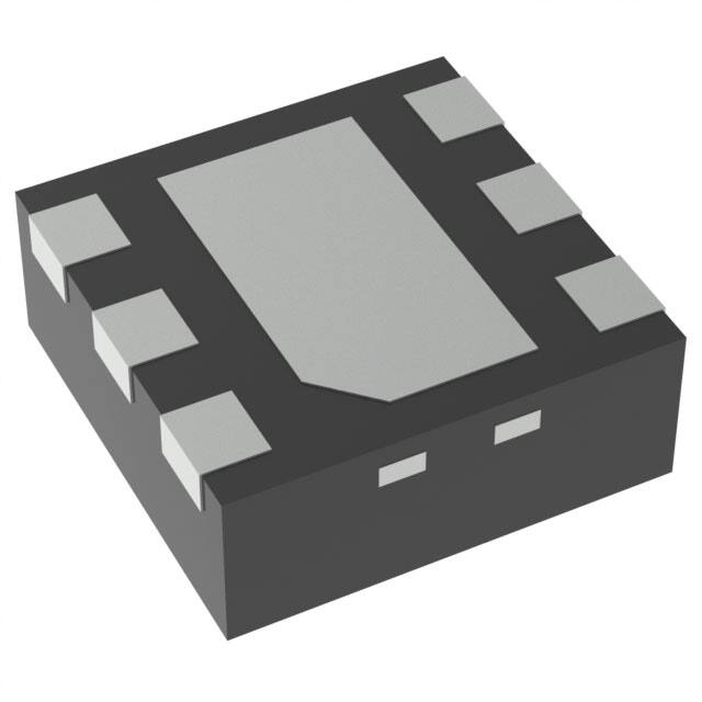
DRV PACKAGE
2mm x 2mm QFN
(TOP VIEW)
VDD
1
SENSE
2
CT
3
Power
PAD
6
RESET
5
GND
4
MR
1
2
3
Please be aware that an important notice concerning availability, standard warranty, and use in critical applications of Texas
Instruments semiconductor products and disclaimers thereto appears at the end of this data sheet.
PowerPAD is a trademark of Texas Instruments.
All other trademarks are the property of their respective owners.
PRODUCTION DATA information is current as of publication date.
Products conform to specifications per the terms of the Texas
Instruments standard warranty. Production processing does not
necessarily include testing of all parameters.
Copyright © 2008, Texas Instruments Incorporated
�TPS3818
SBVS106A – MAY 2008 – REVISED AUGUST 2008 ......................................................................................................................................................... www.ti.com
This integrated circuit can be damaged by ESD. Texas Instruments recommends that all integrated circuits be handled with
appropriate precautions. Failure to observe proper handling and installation procedures can cause damage.
ESD damage can range from subtle performance degradation to complete device failure. Precision integrated circuits may be more
susceptible to damage because very small parametric changes could cause the device not to meet its published specifications.
ORDERING INFORMATION (1)
(1)
(2)
PRODUCT
NOMINAL SUPPLY VOLTAGE (2)
THRESHOLD VOLTAGE (VIT)
TPS3818G01
Adjustable
0.405V
TPS3818G09
0.9V
0.84V
TPS3818G12
1.2V
1.12V
TPS3818G125
1.25V
1.16V
TPS3818G15
1.5V
1.40V
TPS3818G18
1.8V
1.67V
TPS3818G25
2.5V
2.33V
TPS3818G30
3.0V
2.79V
TPS3818G33
3.3V
3.07V
TPS3818G50
5.0V
4.65V
For the most current package and ordering information see the Package Option Addendum at the end of this document, or see the TI
web site at www.ti.com.
Custom threshold voltages from 0.82V to 3.3V, 4.4V to 5.0V are available through the use of factory EEPROM programming. Minimum
order quantities apply. Contact factory for details and availability.
ABSOLUTE MAXIMUM RATINGS (1)
Over operating junction temperature range, unless otherwise noted.
Input voltage range, VDD
CT voltage range, VCT
Other voltage ranges: VRESET, VMR, VSENSE
TPS3818
UNIT
–0.3 to 7.0
V
–0.3 to VDD + 0.3
V
–0.3 to 7
V
5
mA
Operating junction temperature range, TJ (2)
–40 to +150
°C
Storage temperature range, TSTG
–65 to +150
°C
ESD rating, HBM
2
kV
ESD rating, CDM
500
V
RESET pin current
(1)
(2)
2
Stresses beyond those listed under absolute maximum ratings may cause permanent damage to the device. These are stress ratings
only, and functional operation of the device at these or any other conditions beyond those indicated under the Electrical Characteristics
is not implied. Exposure to absolute maximum rated conditions for extended periods may affect device reliability.
As a result of the low dissipated power in this device, it is assumed that TJ = TA.
Submit Documentation Feedback
Copyright © 2008, Texas Instruments Incorporated
Product Folder Link(s): TPS3818
�TPS3818
www.ti.com ......................................................................................................................................................... SBVS106A – MAY 2008 – REVISED AUGUST 2008
ELECTRICAL CHARACTERISTICS
1.7V ≤ VDD ≤ 6.5V, RLRESET = 100kΩ, CLRESET = 50pF, over operating temperature range (TJ = –40°C to +125°C), unless
otherwise noted. Typical values are at TJ = +25°C.
PARAMETER
VDD
TEST CONDITIONS
–40°C < TJ < +125°C
Input supply range
IDD
0°C < TJ < +85°C
Supply current (current into VDD pin)
VOL
Low-level output voltage
Power-up reset voltage (1)
Negative-going
input threshold
accuracy
VIT
MIN
1.65
6.5
5.0
µA
VDD = 6.5V, RESET not asserted
MR, RESET, CT open
2.7
6.0
µA
1.3V ≤ VDD < 1.8V, IOL = 0.4mA
0.3
V
1.8V ≤ VDD ≤ 6.5V, IOL = 1.0mA
0.4
V
VOL (max) = 0.2V, IRESET = 15µA
0.8
V
±1.0
+2.0
VIT ≤ 3.3V
–1.5
±0.5
+1.5
3.3V < VIT ≤ 5.0V
–2.0
±1.0
+2.0
VIT ≤ 3.3V
–40°C < TJ < +85°C
–1.25
±0.5
+1.25
3.3V < VIT ≤ 5.0V
–40°C < TJ < +85°C
–1.5
±0.5
+1.5
1.5
3.0
1.0
2.0
1.0
2.5
RMR
MR Internal pull-up resistance
IOH
RESET leakage current
–40°C < TJ < +85°C
Fixed versions
70
TPS3818G01
VSENSE = VIT
Fixed versions
VSENSE = 6.5V
90
–25
300
VIN = 0V to VDD
5
Other pins
VIN = 0V to 6.5V
5
CIN
Input capacitance,
any pin
VIL
MR logic low input
VIH
MR logic high input
tw
Input pulse width
to RESET
td
RESET delay time (2)
VCT
CT pin (RESET delay time) comparator
threshold (3)
ICT
CT pin (RESET delay time) charging
current (3)
RCT= 2MΩ (resistor between CT and
GND)
0
0.3 VDD
VDD
VIH = 1.05VIT, VIL = 0.95VIT
20
MR
VIH = 0.7VDD, VIL = 0.3VDD
0.001
See Timing Diagram
CT = VDD
nA
nA
pF
0.7 VDD
SENSE
%VIT
µA
1.7
VRESET = 6.5V, RESET not asserted
%
kΩ
25
CT pin
CT = Open
V
2.4
–2.0
Hysteresis on VIT pin
UNIT
VDD = 3.3V, RESET not asserted
MR, RESET, CT open
TPS3818G01
VHYS
Input current at
SENSE pin
MAX
6.5
TPS3818G01
ISENSE
TYP
1.7
V
µs
12
20
28
ms
180
300
420
ms
1.211
1.23
1.249
V
190
220
250
nA
Propagation delay
MR to RESET
VIH = 0.7VDD, VIL = 0.3VDD
150
ns
tpHL
High to low level
RESET delay
SENSE to RESET
VIH = 1.05VIT, VIL = 0.95VIT
20
µs
θJA
Thermal resistance, junction-to-ambient
290
°C/W
(1)
(2)
(3)
The lowest supply voltage (VDD) at which RESET becomes active. Trise(VDD) ≥ 15µs/V.
The delay time accuracy without external capacitor is the same as that of the TPS3808xxx. This specification is included here for
TPS3808xxx device comparison.
The combined RESET delay time accuracy from VCT and ICT is ±15%.
Submit Documentation Feedback
Copyright © 2008, Texas Instruments Incorporated
Product Folder Link(s): TPS3818
3
�TPS3818
SBVS106A – MAY 2008 – REVISED AUGUST 2008 ......................................................................................................................................................... www.ti.com
FUNCTIONAL BLOCK DIAGRAMS
VDD
VDD
VDD
VDD
TPS3818G01
Adjustable Voltage
90kW
90kW
RESET
MR
SENSE
Reset
Logic
Timer
SENSE
RESET
MR
Reset
Logic
Timer
R1
-
-
CT
+
CT
+
R2
0.4V
VREF
0.4V
VREF
R1 + R2 = 4MW
GND
GND
Adjustable Voltage Version
Fixed Voltage Version
Figure 1. Adjustable and Fixed Voltage Versions
PIN ASSIGNMENTS
DBV PACKAGE
SOT23
(TOP VIEW)
6
DRV PACKAGE
2mm × 2mm QFN
(TOP VIEW)
RESET
1
GND
2
5
SENSE
MR
3
4
CT
VDD
VDD
1
SENSE
2
CT
3
Power
PAD
6
RESET
5
GND
4
MR
Table 1. TERMINAL FUNCTIONS
TERMINAL
NAME
SOT23 (DBV)
PIN NO.
RESET
1
RESET is an open-drain output that is driven to a low impedance state when RESET is asserted (either the
SENSE input is lower than the threshold voltage (VIT) or the MR pin is set to a logic low). RESET remains
low (asserted) for the reset period after both SENSE is above VIT and MR is set to a logic high. A pull-up
resistor from 10kΩ to 1MΩ should be used on this pin, and allows the reset pin to attain voltages higher than
VDD.
GND
2
Ground
MR
3
Driving the manual reset pin (MR) low asserts RESET. MR is internally tied to VDD by a 90kΩ pull-up
resistor.
CT
4
Reset period programming pin. Connecting this pin to VDD through a 40kΩ to 200kΩ resistor or leaving it
open results in fixed delay times (see Electrical Characteristics). Connecting this pin to a ground referenced
capacitor ≥ 100pF gives a user-programmable delay time. See the Selecting the Reset Delay Time section
for more information.
SENSE
5
This pin is connected to the voltage to be monitored. If the voltage at this terminal drops below the threshold
voltage VIT, then RESET is asserted.
VDD
6
Supply voltage. It is good analog design practice to place a 0.1µF ceramic capacitor close to this pin.
PowerPAD
4
DESCRIPTION
PowerPAD. Connect to ground plane to enhance thermal performance of package.
Submit Documentation Feedback
Copyright © 2008, Texas Instruments Incorporated
Product Folder Link(s): TPS3818
�TPS3818
www.ti.com ......................................................................................................................................................... SBVS106A – MAY 2008 – REVISED AUGUST 2008
TIMING DIAGRAM
VDD
0.8V
0.0V
RESET
tD = Reset Delay
tD
tD
tD
= Undefined State
SENSE
VIT + VHYS
VIT
MR
0.7VDD
0.3VDD
Time
Figure 2. TPS3818 Timing Diagram Showing MR and SENSE Reset Timing
TRUTH TABLE
MR
SENSE > VIT
RESET
L
0
L
L
1
L
H
0
L
H
1
H
Submit Documentation Feedback
Copyright © 2008, Texas Instruments Incorporated
Product Folder Link(s): TPS3818
5
�TPS3818
SBVS106A – MAY 2008 – REVISED AUGUST 2008 ......................................................................................................................................................... www.ti.com
TYPICAL CHARACTERISTICS
At TJ = +25°C, VDD = 3.3V, RLRESET = 100kΩ, and CLRESET = 50pF, unless otherwise noted.
SUPPLY CURRENT
vs
SUPPLY VOLTAGE
RESET TIMEOUT PERIOD
vs
CT
4.0
100
3.5
IDD (µA)
RESET Timeout (sec)
+125_ C
3.0
+85_ C
2.5
2.0
+25_C
1.5
1.0
10
−40°C, +25°C, +125°C
1
0.1
0.01
− 40_ C
0.5
0
0
1
2
3
4
5
6
0.001
0.0001
7
0.001
0.01
VDD (V)
NORMALIZED RESET TIMEOUT PERIOD
vs
TEMPERATURE
(CT = OPEN, CT = VDD, CT = Any)
MAXIMUM TRANSIENT DURATION AT SENSE
vs
SENSE THRESHOLD OVERDRIVE VOLTAGE
100
Transient Duration below VIT (µs)
Normalized RESET Timeout Period (%)
8
6
4
2
0
−2
−4
−6
−8
RESET OCCURS
ABOVE THE CURVE
10
1
−10
−30
−10
10
30
50
70
90
110
0
130
5
10
15
25
30
35
40
Figure 6.
NORMALIZED SENSE THRESHOLD VOLTAGE (VIT)
vs
TEMPERATURE
LOW-LEVEL RESET VOLTAGE
vs
RESET CURRENT
45
50
4.5
VOL Low−Level RESET Voltage (V)
1.0
0.8
0.6
Normalized VIT (%)
20
Overdrive (%VIT)
Figure 5.
0.4
0.2
0
−0.2
−0.4
−0.6
−0.8
−1.0
−50
10
Figure 4.
Temperature (°C)
4.0
3.5
3.0
2.5
2.0
VDD = 1.8V
1.5
1.0
0.5
0
−30
−10
10
30
50
70
90
110
130
0
Temperature (°C)
Figure 7.
6
1
Figure 3.
10
−50
0.1
CT (µF)
0.5
1.0
1.5
2.0
2.5
RESET Current (mA)
3.0
3.5
4.0
Figure 8.
Submit Documentation Feedback
Copyright © 2008, Texas Instruments Incorporated
Product Folder Link(s): TPS3818
�TPS3818
www.ti.com ......................................................................................................................................................... SBVS106A – MAY 2008 – REVISED AUGUST 2008
TYPICAL CHARACTERISTICS (continued)
At TJ = +25°C, VDD = 3.3V, RLRESET = 100kΩ, and CLRESET = 50pF, unless otherwise noted.
LOW-LEVEL RESET VOLTAGE
vs
RESET CURRENT
VOL Low−Level RESET Voltage (V)
0.8
0.7
0.6
0.5
0.4
VDD = 3.3V
0.3
0.2
0.1
VDD = 6.5V
0
0
0.5
1.0
1.5
2.0
2.5
3.0
3.5
4.0
4.5
5.0
RESET Current (mA)
Figure 9.
Submit Documentation Feedback
Copyright © 2008, Texas Instruments Incorporated
Product Folder Link(s): TPS3818
7
�TPS3818
SBVS106A – MAY 2008 – REVISED AUGUST 2008 ......................................................................................................................................................... www.ti.com
DEVICE OPERATION
The TPS3818 microprocessor supervisory product
family is designed to assert a RESET signal when
either the SENSE pin voltage drops below VIT or the
manual reset (MR) is driven low. The RESET output
remains asserted for a user-adjustable time after both
the manual reset (MR) and SENSE voltages return
above the respective thresholds. A broad range of
voltage threshold and reset delay time adjustments
are available, allowing these devices to be used in a
wide array of applications. Reset threshold voltages
can be factory-set from 0.82V to 3.3V or from 4.4V to
5.0V, while the TPS3818G01 can be set to any
voltage above 0.405V using an external resistor
divider. Two preset delay times are also
user-selectable: connecting the CT pin to VDD results
in a 300ms reset delay, while leaving the CT pin open
yields a 20ms reset delay. In addition, connecting a
capacitor between CT and GND allows the designer
to select any reset delay period from 1.25ms to 10s.
supply line can be used to allow the reset signal for
the microprocessor to have a voltage higher than VDD
(up to 6.5V). The pull-up resistor should be no
smaller than 10kΩ as a result of the finite impedance
of the RESET line.
SENSE INPUT
The SENSE input provides a terminal at which any
system voltage can be monitored. If the voltage on
this pin drops below VIT, then RESET is asserted.
The comparator has a built-in hysteresis to ensure
smooth RESET assertions and de-assertions. It is
good analog design practice to put a 1nF to 10nF
bypass capacitor on the SENSE input to reduce
sensitivity to transients and layout parasitics.
The TPS3818G01 can be used to monitor any
voltage rail down to 0.405V using the circuit shown in
Figure 11.
VIN
RESET OUTPUT
A typical application of the TPS3818G25 used with
the OMAP1510 processor is shown in Figure 10. The
open-drain RESET output is typically connected to
the RESET input of a microprocessor. A pull-up
resistor must be used to hold this line high when
RESET is not asserted. The RESET output is
undefined for voltage below 0.8V, but this is normally
not a problem because most microprocessors do not
function below this voltage. RESET remains high
(unasserted) as long as SENSE is above its threshold
(VIT) and the manual reset (MR) is logic high. If either
SENSE falls below VIT or MR is driven low, RESET is
asserted, driving the RESET pin to a low impedance.
2.5V
VDDSHV 1, 3, 6, 7, 9
SENSE VDD
TPS3818G25
MR
CT
1MW
RESET
GND
OMAP1510
RESPWRON
GND
Figure 10. Typical Application of the TPS3818
with an OMAP Processor
Once MR is again logic high and SENSE is above VIT
+ VHYS (the threshold hysteresis), a delay circuit is
enabled that holds RESET low for a specified reset
delay period. Once the reset delay has expired, the
RESET pin goes to a high impedance state. The
pull-up resistor from the open-drain RESET to the
8
VOUT
VDD
VIT¢ = (1 +
R1
R1
) 0.405
R2
TPS3818G01
SENSE
RESET
1nF
R2
GND
Figure 11. Using the TPS3818G01 to Monitor a
User-Defined Threshold Voltage
MANUAL RESET (MR) INPUT
The manual reset (MR) input allows a processor or
other logic circuit to initiate a reset. A logic low
(0.3VDD) on MR causes RESET to assert. After MR
returns to a logic high and SENSE is above its reset
threshold, RESET is de-asserted after the
user-defined reset delay expires. Note that MR is
internally tied to VDD using a 90kΩ resistor so this pin
can be left unconnected if MR is not used.
See Figure 12 for how MR can be used to monitor
multiple system voltages. Note that if the logic signal
driving MR does not go fully to VDD, there will be
some additional current draw into VDD as a result of
the internal pull-up resistor on MR. To minimize
current draw, a logic-level FET can be used as
illustrated in Figure 13.
Submit Documentation Feedback
Copyright © 2008, Texas Instruments Incorporated
Product Folder Link(s): TPS3818
�TPS3818
www.ti.com ......................................................................................................................................................... SBVS106A – MAY 2008 – REVISED AUGUST 2008
1.2V
by the choice of resistor. Figure 14b shows a fixed
20ms delay time by leaving the CT pin open.
Figure 14c shows a ground referenced capacitor
connected to CT for a user-defined program time
between 1.25ms and 10s.
3.3V
SENSE VDD
SENSE VDD
TPS3818G25
TPS3818G33
RESET
CT
RESET
MR
CT
GND
VI/O
VCORE
The capacitor CT should be ≥ 100pF nominal value in
order for the TPS3818xxx to recognize that the
capacitor is present. The capacitor value for a given
delay time can be calculated using the following
equation:
DSP
GPIO
GND
GND
C T (nF) + ƪt D (s)*0.5
10*3 (s)ƫ
175
(1)
The reset delay time is determined by the time it
takes an on-chip precision 220nA current source to
charge the external capacitor to 1.23V. When a
RESET is asserted the capacitor is discharged. When
the RESET conditions are cleared, the internal
current source is enabled and begins to charge the
external capacitor. When the voltage on this capacitor
reaches 1.23V, RESET is de-asserted. Note that a
low leakage type capacitor such as a ceramic should
be used, and that stray capacitance around this pin
may cause errors in the reset delay time.
Figure 12. Using MR to Monitor Multiple System
Voltages
3.3V
V DD SENSE
90kW
MR
TPS3818xxx
IMMUNITY TO SENSE PIN VOLTAGE
TRANSIENTS
GND
The TPS3818 is relatively immune to short negative
transients on the SENSE pin. Sensitivity to transients
depends on threshold overdrive, as shown in the
Maximum Transient Duration at Sense vs Sense
Threshold Overdrive Voltage graph (Figure 6) in the
Typical Characteristics section.
Figure 13. Using an External MOSFET to Minimize
IDD When MR Signal Does Not Go to VDD
SELECTING THE RESET DELAY TIME
The TPS3818 has three options for setting the
RESET delay time as shown in Figure 14. Figure 14a
shows the configuration for a fixed 300ms typical
delay time by tying CT to VDD; a resistor from 40kΩ to
200kΩ must be used. Supply current is not affected
3.3V
3.3V
50kW
3.3V
SENSE VDD
SENSE VDD
SENSE VDD
TPS3818G33
TPS3818G33
TPS3818G33
CT
CT
RESET
CT
RESET
RESET
CT
300ms Delay
20ms Delay
Delay (s) =
(b)
(a)
CT (nF)
-3
+ 0.5 ´ 10 (s)
175
(c)
Figure 14. Configuration Used to Set the RESET Delay Time
Submit Documentation Feedback
Copyright © 2008, Texas Instruments Incorporated
Product Folder Link(s): TPS3818
9
�PACKAGE OPTION ADDENDUM
www.ti.com
10-Dec-2020
PACKAGING INFORMATION
Orderable Device
Status
(1)
Package Type Package Pins Package
Drawing
Qty
Eco Plan
(2)
Lead finish/
Ball material
MSL Peak Temp
Op Temp (°C)
Device Marking
(3)
(4/5)
(6)
TPS3818G25DRVT
ACTIVE
WSON
DRV
6
250
RoHS & Green
NIPDAU
Level-1-260C-UNLIM
-40 to 125
CHJ
(1)
The marketing status values are defined as follows:
ACTIVE: Product device recommended for new designs.
LIFEBUY: TI has announced that the device will be discontinued, and a lifetime-buy period is in effect.
NRND: Not recommended for new designs. Device is in production to support existing customers, but TI does not recommend using this part in a new design.
PREVIEW: Device has been announced but is not in production. Samples may or may not be available.
OBSOLETE: TI has discontinued the production of the device.
(2)
RoHS: TI defines "RoHS" to mean semiconductor products that are compliant with the current EU RoHS requirements for all 10 RoHS substances, including the requirement that RoHS substance
do not exceed 0.1% by weight in homogeneous materials. Where designed to be soldered at high temperatures, "RoHS" products are suitable for use in specified lead-free processes. TI may
reference these types of products as "Pb-Free".
RoHS Exempt: TI defines "RoHS Exempt" to mean products that contain lead but are compliant with EU RoHS pursuant to a specific EU RoHS exemption.
Green: TI defines "Green" to mean the content of Chlorine (Cl) and Bromine (Br) based flame retardants meet JS709B low halogen requirements of