Order
Now
Product
Folder
Support &
Community
Tools &
Software
Technical
Documents
TPS3820, TPS3823, TPS3823A, TPS3824, TPS3825, TPS3828
SLVS165L – APRIL 1998 – REVISED JANUARY 2018
TPS382x Voltage Monitor With Watchdog Timer
1 Features
3 Description
•
The TPS382x family of supervisors provide circuit
initialization and timing supervision, primarily for DSP
and processor-based systems. During power on,
RESET asserts when the supply voltage VDD
becomes greater than 1.1 V. Thereafter, the supply
voltage supervisor monitors VDD and keeps RESET
active low as long as VDD remains less than the
threshold voltage, VIT−. An internal timer delays the
return of the output to the inactive state (high) to
ensure proper system reset. The delay time, td, starts
after VDD has risen above the threshold voltage (VIT−
+ VHYS). When the supply voltage drops below the
threshold voltage VIT−, the output becomes active
(low) again. No external components are required. All
the devices of this family have a fixed-sense
threshold voltage, VIT–, set by an internal voltage
divider. The TPS382x family also offers watchdog
time out options of 200 ms (TPS3820) and 1.6 s
(TPS3823/4/8).
•
•
•
•
•
•
•
Power-On Reset Generator With Fixed Delay
Time of 200 ms (TPS3823/4/5/8) or 25 ms
(TPS3820)
Manual Reset Input (TPS3820/3/5/8)
Reset Output Available in Active-Low
(TPS3820/3/4/5), Active-High (TPS3824/5), and
Open Drain (TPS3828)
Supply Voltage Supervision Range:
2.5 V, 3 V, 3.3 V, 5 V
Watchdog Timer (TPS3820/3/4/8)
Supply Current of 15 μA (Typical)
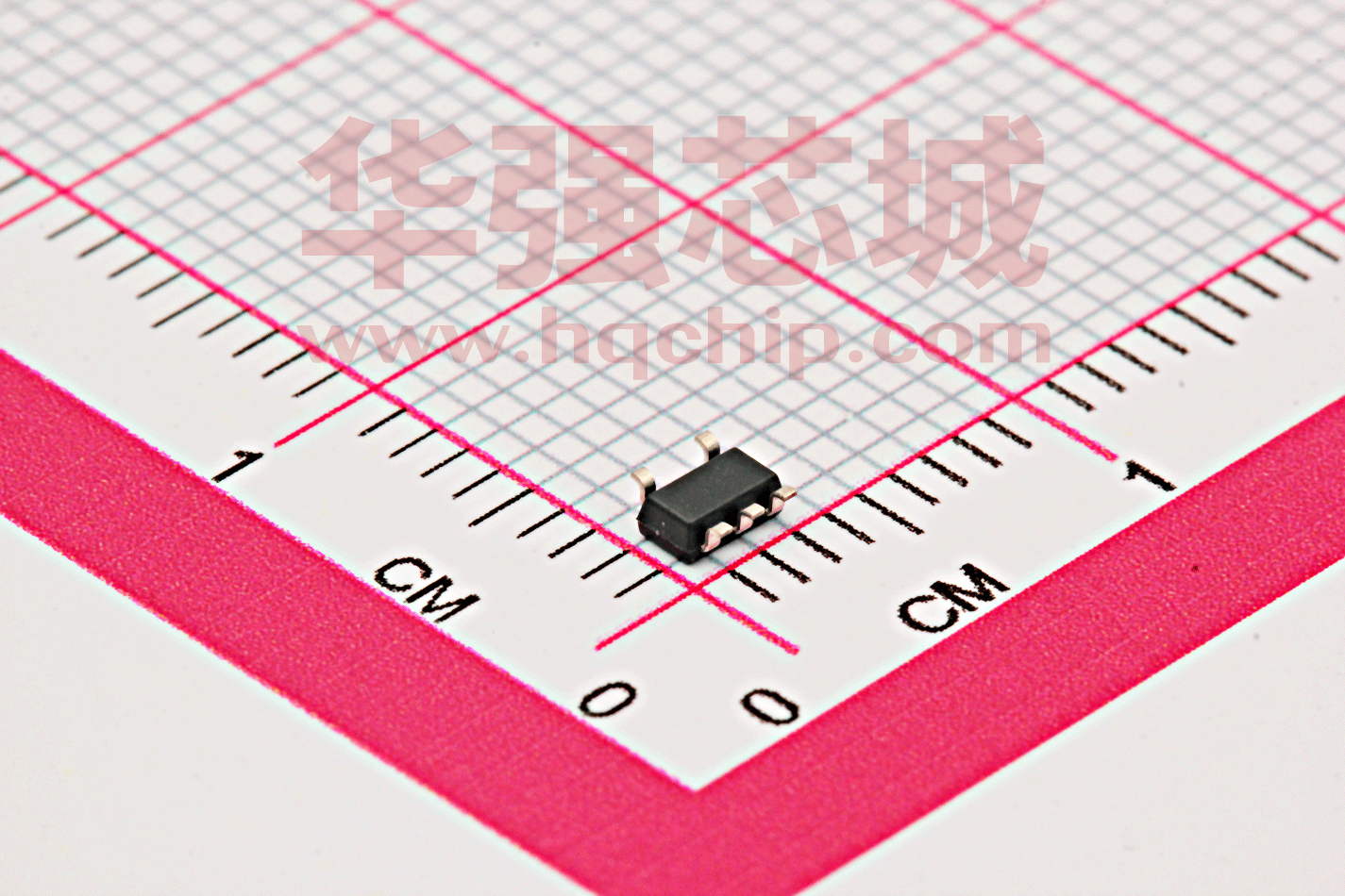
5-Pin SOT-23 Package
Temperature Range: −40°C to 85°C
2 Applications
•
•
•
•
•
•
•
•
DSPs, Microcontrollers, or Microprocessors
Industrial Equipment
Programmable Controls
Automotive Systems
Portable and Battery-Powered Equipment
Intelligent Instruments
Wireless Communications Systems
Notebook and Desktop Computers
Typical Application Schematic
3.3 V
100 nF
VDD
RESET
VDD
RESET
TPS3823-33
WDI
MR
GND
MSP430C325
I/O
GND
Device Information(1)
PART NUMBER
TPS382x
PACKAGE
BODY SIZE (NOM)
SOT-23 (5)
2.90 mm × 1.60 mm
(1) For all available packages, see the orderable addendum at
the end of the data sheet.
Normalized Input Threshold Voltage vs Free-Air
Temperature
Normalized Input Threshold Voltage −V IT (TA), VIT (25°C)
1
1.001
1
0.999
0.998
0.997
0.996
0.995
−40
−15
10
35
60
85
TA − Free-Air Temperature − °C
1
An IMPORTANT NOTICE at the end of this data sheet addresses availability, warranty, changes, use in safety-critical applications,
intellectual property matters and other important disclaimers. PRODUCTION DATA.
�TPS3820, TPS3823, TPS3823A, TPS3824, TPS3825, TPS3828
SLVS165L – APRIL 1998 – REVISED JANUARY 2018
www.ti.com
Table of Contents
1
2
3
4
5
6
7
8
Features ..................................................................
Applications ...........................................................
Description .............................................................
Revision History.....................................................
Device Comparison Table.....................................
Pin Configuration and Functions .........................
Specifications.........................................................
1
1
1
2
4
4
5
7.1
7.2
7.3
7.4
7.5
7.6
7.7
7.8
5
5
5
5
6
7
7
8
Absolute Maximum Ratings ......................................
ESD Ratings ............................................................
Recommended Operating Conditions.......................
Thermal Information ..................................................
Electrical Characteristics...........................................
Timing Requirements ................................................
Switching Characteristics ..........................................
Typical Characteristics ..............................................
Detailed Description ............................................ 10
8.1 Overview ................................................................. 10
8.2 Functional Block Diagram ....................................... 10
8.3 Feature Description................................................. 10
8.4 Device Functional Modes........................................ 11
9
Application and Implementation ........................ 12
9.1 Application Information............................................ 12
9.2 Typical Applications ................................................ 12
10 Power Supply Recommendations ..................... 15
11 Layout................................................................... 15
11.1 Layout Guidelines ................................................. 15
11.2 Layout Example .................................................... 15
12 Device and Documentation Support ................. 16
12.1
12.2
12.3
12.4
12.5
12.6
12.7
Device Support......................................................
Documentation Support ........................................
Related Links ........................................................
Community Resources..........................................
Trademarks ...........................................................
Electrostatic Discharge Caution ............................
Glossary ................................................................
16
16
17
17
17
17
17
13 Mechanical, Packaging, and Orderable
Information ........................................................... 17
4 Revision History
NOTE: Page numbers for previous revisions may differ from page numbers in the current version.
Changes from Revision K (November 2015) to Revision L
Page
•
Changed the RESET columns for the TPS3824 and TPS3828 devices................................................................................ 4
•
Removed 'Open-drain' from the RESET column for the TPS3828 device ............................................................................. 4
•
Changed text in the MR pin description from: RESET to: RESET ........................................................................................ 4
Changes from Revision J (April 2013) to Revision K
Page
•
Added ESD Ratings table, Feature Description section, Device Functional Modes, Application and Implementation
section, Power Supply Recommendations section, Layout section, Device and Documentation Support section, and
Mechanical, Packaging, and Orderable Information section ................................................................................................. 1
•
Changed front-page figure...................................................................................................................................................... 1
•
Changed Pin Configuration and Functions section; updated table format ............................................................................. 4
•
Changed "free-air temperature" to "junction temperature" in Absolute Maximum Ratings condition statement ................... 5
•
Deleted Soldering temperature specification from Absolute Maximum Ratings table............................................................ 5
•
Changed clamp current to current specifications in Absolute Maximum Ratings table ......................................................... 5
•
Changed Removed VI from Absolute Maximum Ratings table .............................................................................................. 5
•
Changed Removed VSENSE from Recommended Operating Conditions table........................................................................ 5
•
Changed free-air temperature to junction temperature in Electrical Characteristics condition statement.............................. 6
•
Changed "TA" to "TJ" in Timing Requirements condition statement ...................................................................................... 7
•
Changed "TA" to "TJ" in Switching Characteristics condition statement ................................................................................ 7
•
Added footnote (3) to Functional Block Diagram ................................................................................................................ 10
•
Changed part number shown in Figure 9 ............................................................................................................................ 12
•
Changed Figure 11 .............................................................................................................................................................. 14
2
Submit Documentation Feedback
Copyright © 1998–2018, Texas Instruments Incorporated
Product Folder Links: TPS3820 TPS3823 TPS3824 TPS3825 TPS3828
�TPS3820, TPS3823, TPS3823A, TPS3824, TPS3825, TPS3828
www.ti.com
SLVS165L – APRIL 1998 – REVISED JANUARY 2018
Changes from Revision I (February 2013) to Revision J
Page
•
Added TPS382xA-33 to second RESET row of VOH parameter in Electrical Characteristics table ....................................... 6
•
Added TPS382xA-33 to third RESET row of VOL parameter in Electrical Characteristics table ............................................ 6
•
Corrected typo in VOL RESET parameter test conditions ....................................................................................................... 6
•
Added TPS382xA-33 to third and seventh rows of VIT– parameter in Electrical Characteristics table................................... 6
•
Added TPS382xA-33 to third row of Vhys parameter in Electrical Characteristics table......................................................... 6
•
Added TPS382xA-33 to third row of IOS parameter in Electrical Characteristics table........................................................... 7
•
Added TPS3823A to second row of ttout parameter in Switching Characteristics table.......................................................... 7
•
Added TPS3823A to second row of td parameter in Switching Characteristics table ............................................................ 7
•
Added TPS3823A to first row of tPHL parameter in Switching Characteristics table............................................................... 7
Changes from Revision H (July 2012) to Revision I
•
Page
Added last row of Terminal Functions table to Package Information table ............................................................................ 4
Copyright © 1998–2018, Texas Instruments Incorporated
Submit Documentation Feedback
Product Folder Links: TPS3820 TPS3823 TPS3824 TPS3825 TPS3828
3
�TPS3820, TPS3823, TPS3823A, TPS3824, TPS3825, TPS3828
SLVS165L – APRIL 1998 – REVISED JANUARY 2018
www.ti.com
5 Device Comparison Table
RESET
WDI
MR
TPS3820
DEVICE
RESET
Push-pull
X
X
TPS3823
Push-pull
X
X
Push-pull
X
X
Push-pull
X
TPS3823A
TPS3824
Push-pull
TPS3825
Push-pull
Push-pull
TPS3828
X
Open-drain
X
X
6 Pin Configuration and Functions
TPS3820, TPS3823, TPS3823A, TPS3828: DBV PACKAGE
5-Pin SOT-23
Top View
5
1
RESET
GND
2
MR
3
4
TPS3824: DBV PACKAGE
5-Pin SOT-23
Top View
VDD
RESET
1
GND
2
RESET
3
5
VDD
4
WDI
WDI
TPS3825: DBV PACKAGE
5-Pin SOT-23
Top View
RESET
1
GND
2
RESET
3
5
VDD
4
MR
Pin Functions
PIN
TPS3820,
TPS3823,
TPS3823A,
TPS3828
TPS3824
TPS3825
GND
2
2
2
—
MR
3
—
4
I
Manual-reset input. Pull low to force a reset. RESET remains low as long
as MR is low and for the time-out period after MR goes high. Leave
unconnected or connect to VDD when unused.
RESET
—
3
3
O
Active-high reset output. Either push-pull or open-drain output stage.
RESET
1
1
1
O
Active-low reset output. Either push-pull or open-drain output stage.
VDD
5
5
5
I
Supply voltage. Powers the device and monitors its own voltage.
I
Watchdog timer input. If WDI remains high or low longer than the timeout period, then reset is triggered. The timer clears when reset is
asserted or when WDI sees a rising edge or a falling edge. If unused, the
WDI connection must be high impedance to prevent it from causing a
reset event.
NAME
WDI
4
4
4
Submit Documentation Feedback
—
I/O
DESCRIPTION
Ground connection
Copyright © 1998–2018, Texas Instruments Incorporated
Product Folder Links: TPS3820 TPS3823 TPS3824 TPS3825 TPS3828
�TPS3820, TPS3823, TPS3823A, TPS3824, TPS3825, TPS3828
www.ti.com
SLVS165L – APRIL 1998 – REVISED JANUARY 2018
7 Specifications
7.1 Absolute Maximum Ratings
over operating junction temperature range (unless otherwise noted) (1)
Voltage
Current
(2)
MIN
MAX
VDD
–0.3
6
RESET, RESET, MR, WDI
–0.3
(VDD + 0.3)
Maximum low output, IOL
–5
5
Maximum high output, IOH
–5
5
–10
10
Output range (VO < 0 or VO > VDD), IOK
Continuous total power dissipation
Temperature
(1)
(2)
UNIT
V
mA
See Thermal Information
Operating free-air, TA
–40
85
Storage, Tstg
–65
150
°C
Stresses beyond those listed under Absolute Maximum Ratings may cause permanent damage to the device. These are stress ratings
only, which do not imply functional operation of the device at these or any other conditions beyond those indicated under Recommended
Operating Conditions. Exposure to absolute-maximum-rated conditions for extended periods may affect device reliability.
All voltage values are with respect to GND.
7.2 ESD Ratings
VALUE
V(ESD)
(1)
(2)
Electrostatic
discharge
Human body model (HBM), per ANSI/ESDA/JEDEC JS-001 (1)
±2000
Charged device model (CDM), per JEDEC specification JESD22-C101 (2)
±500
UNIT
V
JEDEC document JEP155 states that 500-V HBM allows safe manufacturing with a standard ESD control process.
JEDEC document JEP157 states that 250-V CDM allows safe manufacturing with a standard ESD control process.
7.3 Recommended Operating Conditions
over operating junction temperature range (unless otherwise noted).
MIN
VDD
Supply voltage
VIH
High-level input voltage at MR and WDI
VIL
Low-level input voltage
Δt/ΔV
Input transition rise and fall rate at MR or WDI
TA
Operating free-air temperature
NOM
MAX
1.1
UNIT
5.5
V
0.7 × VDD
V
0.3 × VDD
–40
V
100
ns/V
85
°C
7.4 Thermal Information
TPS382x
THERMAL METRIC (1)
DBV (SOT-23)
UNIT
5 PINS
RθJA
Junction-to-ambient thermal resistance
209.1
°C/W
RθJC(top)
Junction-to-case (top) thermal resistance
72.8
°C/W
RθJB
Junction-to-board thermal resistance
36.7
°C/W
ψJT
Junction-to-top characterization parameter
2.1
°C/W
ψJB
Junction-to-board characterization parameter
35.8
°C/W
(1)
For more information about traditional and new thermal metrics, see the Semiconductor and IC Package Thermal Metrics application
report (SPRA953).
Copyright © 1998–2018, Texas Instruments Incorporated
Submit Documentation Feedback
Product Folder Links: TPS3820 TPS3823 TPS3824 TPS3825 TPS3828
5
�TPS3820, TPS3823, TPS3823A, TPS3824, TPS3825, TPS3828
SLVS165L – APRIL 1998 – REVISED JANUARY 2018
www.ti.com
7.5 Electrical Characteristics
over operating junction temperature range (unless otherwise noted)
PARAMETER
RESET
VOH
High-level output voltage
RESET
TEST CONDITIONS
TPS382x-25
VDD = VIT− + 0.2 V, IOH = –20 μA
TPS382x-30
TPS382x-33
TPS382xA-33
VDD = VIT− + 0.2 V, IOH = –30 μA
TPS382x-50
VDD = VIT− + 0.2 V IOH = –120 μA
TPS3824-25
TPS3825-25
VDD ≥ 1.8 V, IOH = –100 μA
MIN
MAX
UNIT
0.8 × VDD
VDD − 1.5 V
V
TPS3824-30
TPS3825-30
TPS3824-33
TPS3825-33
TYP
0.8 × VDD
VDD ≥ 1.8 V, IOH = –150 μA
TPS3824-50
TPS3825-50
TPS3824-25
TPS3825-25
RESET
VOL
Low-level output voltage
TPS3824-30
TPS3825-30
TPS3824-33
TPS3825-33
VDD = VIT− + 0.2 V, IOL = 1 mA
VDD = VIT− + 0.2 V, IOL = 1.2 mA
TPS3824-50
TPS3825-50
VDD = VIT− + 0.2 V, IOL = 3 mA
TPS382x-25
VDD = VIT− – 0.2 V, IOL = 1 mA
0.4
V
TPS382x-30
RESET
TPS382x-33
TPS382xA-33
VDD = VIT− – 0.2 V, IOL = 1.2 mA
TPS382x-50
VDD = VIT− – 0.2 V, IOL = 3 mA
Power-up reset voltage (1)
0.4
VDD ≥ 1.1 V, IOL = 20 μA
0.4
TPS382x-25
2.21
2.25
2.30
2.59
2.63
2.69
2.88
2.93
3
TPS382x-50
4.49
4.55
4.64
TPS382x-25
2.20
2.25
2.30
2.57
2.63
2.69
2.86
2.93
3
4.46
4.55
4.64
TPS382x-30
TPS382x-33
TPS382xA-33
Negative-going input
threshold voltage (2)
VIT−
TA = 0°C to 85°C
TPS382x-30
TPS382x-33
TPS382xA-33
TA = –40°C to 85°C
TPS382x-50
V
V
TPS382x-25
TPS382x-30
Vhys
Hysteresis at VDD input
IIH(AV)
Average high-level input current
IIL(AV)
Average low-level input current
IIH
High-level input current
IIL
Low-level input current
30
TPS382x-50
(1)
(2)
6
mV
TPS382x-33
TPS382xA-33
50
WDI = VDD, time average (DC = 88%)
120
WDI = 0.3 V, VDD = 5.5 V time average (DC = 12%)
–15
WDI
WDI = VDD
140
190
MR
MR = VDD × 0.7, VDD = 5.5 V
–40
–60
WDI
WDI = 0.3 V, VDD = 5.5 V
140
190
MR
MR = 0.3 V, VDD = 5.5 V
–110
–160
WDI
µA
µA
µA
The lowest supply voltage at which RESET becomes active. tr, VDD ≥ 15 μs/V.
To ensure best stability of the threshold voltage, a bypass capacitor (ceramic, 0.1 μF) must be placed near the supply terminals.
Submit Documentation Feedback
Copyright © 1998–2018, Texas Instruments Incorporated
Product Folder Links: TPS3820 TPS3823 TPS3824 TPS3825 TPS3828
�TPS3820, TPS3823, TPS3823A, TPS3824, TPS3825, TPS3828
www.ti.com
SLVS165L – APRIL 1998 – REVISED JANUARY 2018
Electrical Characteristics (continued)
over operating junction temperature range (unless otherwise noted)
PARAMETER
TEST CONDITIONS
MIN
TYP
MAX
UNIT
TPS382x-25
TPS382x-30
IOS
Output short-circuit
current (3)
IDD
Supply current
RESET
TPS382x-33
TPS382xA-33
–400
VDD = VIT, max + 0.2 V, VO = 0 V
TPS382x-50
–800
WDI, MR, and outputs unconnected
15
Internal pullup resistor at MR
Ci
(3)
µA
Input capacitance at MR, WDI
VI = 0 V to 5.5 V
25
µA
52
kΩ
5
pF
The RESET short-circuit current is the maximum pullup current when RESET is driven low by a microprocessor bidirectional reset pin.
7.6 Timing Requirements
At RL = 1 MΩ, CL = 50 pF, and TJ = 25°C, unless otherwise noted.
MIN
tw
Pulse width
TYP
MAX
UNIT
at VDD
VDD = VIT− + 0.2 V, VDD = VIT– – 0.2 V
6
at MR
VDD ≥ VIT− + 0.2 V, VIL = 0.3 × VDD, VIH = 0.7 × VDD
1
μs
at WDI
VDD ≥ VIT− + 0.2 V, VIL = 0.3 × VDD, VIH = 0.7 × VDD
100
ns
μs
7.7 Switching Characteristics
At RL = 1 MΩ, CL = 50 pF, and TJ = 25°C, unless otherwise noted.
PARAMETER
ttout
td
tPHL
tPLH
Watchdog time out
TPS3823/4/8, TPS3823A
TPS3820
Delay time
TPS3823/4/5/8, TPS3823A
Propagation (delay) time,
high-to-low-level output
Propagation (delay) time,
low-to-high-level output
VDD
TEST CONDITIONS
TPS3820
MIN
TYP
MAX
UNIT
VDD ≥ VIT− + 0.2 V
See Figure 1
112
200
300
ms
0.9
1.6
2.5
s
VDD ≥ VIT− + 0.2 V
See Figure 1
15
25
37
120
200
300
MR to RESET delay
(TPS3820/3/5/8, TPS3823A)
VDD ≥ VIT− + 0.2 V,
VIL = 0.3 × VDD,
VIH = 0.7 × VDD
0.1
VDD to RESET delay
VIL = VIT– – 0.2 V,
VIH = VIT– + 0.2 V
25
MR to RESET delay (TPS3824/5)
VDD ≥ VIT− + 0.2 V,
VIL = 0.3 × VDD,
VIH = 0.7 × VDD
0.1
VDD to RESET delay (TPS3824/5)
VIL = VIT– – 0.2 V,
VIH = VIT– + 0.2 V
25
ms
µs
µs
VIT1.1 V
td
td
tt(out)
td
undefined
undefined
RESET
WDI
Figure 1. Timing Diagram
Copyright © 1998–2018, Texas Instruments Incorporated
Submit Documentation Feedback
Product Folder Links: TPS3820 TPS3823 TPS3824 TPS3825 TPS3828
7
�TPS3820, TPS3823, TPS3823A, TPS3824, TPS3825, TPS3828
SLVS165L – APRIL 1998 – REVISED JANUARY 2018
www.ti.com
19
1.001
MR = Open
WDI = Open
TA = 25°C
17
15
1
I DD− Supply Current − µ A
Normalized Input Threshold Voltage −V IT (TA), VIT (25°C)
7.8 Typical Characteristics
0.999
0.998
0.997
13
TPS382x-33
11
9
7
5
3
0.996
1
0.995
−40
−15
10
60
35
−1
−0.5
85
0.5
1.5
VOL − Low-Level Output Voltage − V
VDD = 5.5 V
WDI = Open
I I − Input Current − µ A
0
−40°C
−100
85°C
−150
2.5
2
1.5
85°C
1
−40°C
0.5
0
0
1
2
3
4
5
0
6
2
1
3
4
5
6
7
8
9
10
IOL − Low-Level Output Current − mA
Figure 4. Input Current vs Input Voltage at MR
Figure 5. Low-Level Output Voltage vs Low-Level Output
Current
6
3.5
VDD = 3.2 V
WDI = Open
MR = Open
3
VOH − High-Level Output Voltage − V
VOH − High-Level Output Voltage − V
6.5
VDD = 2.66 V
WDI = Open
MR = Open
VI − Input Voltage at MR − V
2.5
−40°C
2
1.5
85°C
1
0.5
0
VDD = 5.5 V
WDI = Open
MR = Open
5
4
−40°C
3
85°C
2
1
0
0
−50
−100
−150
−200
−250
IOH − High-Level Output Current − µA
Figure 6. High-Level Output Voltage vs High-Level Output
Current
8
5.5
4.5
3
50
−200
−1
3.5
Figure 3. Supply Current vs Supply Voltage
Figure 2. Normalized Input Threshold Voltage vs Free-Air
Temperature at VDD
−50
2.5
VDD − Supply Voltage − V
TA − Free-Air Temperature − °C
Submit Documentation Feedback
0
−100
−200
−300
−400
−500
−600
−700
IOH − High-Level Output Current − µA
Figure 7. High-Level Output Voltage vs High-Level Output
Current
Copyright © 1998–2018, Texas Instruments Incorporated
Product Folder Links: TPS3820 TPS3823 TPS3824 TPS3825 TPS3828
�TPS3820, TPS3823, TPS3823A, TPS3824, TPS3825, TPS3828
www.ti.com
SLVS165L – APRIL 1998 – REVISED JANUARY 2018
Typical Characteristics (continued)
t w − Minimum Pulse Duration at VDD − µs
10
WDI = Open
MR = Open
8
6
4
2
0
0
200
400
600
800
1000
VDD − Threshold Overdrive − mV
Figure 8. Minimum Pulse Duration at VDD vs VDD Threshold Overdrive
Copyright © 1998–2018, Texas Instruments Incorporated
Submit Documentation Feedback
Product Folder Links: TPS3820 TPS3823 TPS3824 TPS3825 TPS3828
9
�TPS3820, TPS3823, TPS3823A, TPS3824, TPS3825, TPS3828
SLVS165L – APRIL 1998 – REVISED JANUARY 2018
www.ti.com
8 Detailed Description
8.1 Overview
The TPS382x family of supervisors provide circuit initialization and timing supervision. Optional configurations
include devices with active-high and active-low output signals (TPS3824/5), devices with a watchdog timer
(TPS3820/3/4/8), and devices with manual reset (MR) pins (TPS3820/3/5/8). RESET asserts when the supply
voltage, VDD, rises above 1.1 V. For devices with active-low output logic, the device monitors VDD and keeps
RESET low as long as VDD remains below the negative threshold voltage, VIT−. For devices with active-high
output logic, RESET remains high as long as VDD remains below VIT−. An internal timer delays the return of the
output to the inactive state (high) to ensure proper system reset. The delay time, td, starts after VDD rises above
the positive threshold voltage (VIT− + VHYS). When the supply voltage drops below VIT−, the output becomes
active (low) again. All the devices of this family have a fixed-sense threshold voltage, VIT–, set by an internal
voltage divider, so no external components are required.
The TPS382x family is designed to monitor supply voltages of 2.5 V, 3 V, 3.3 V, and 5 V. The devices are
available in a 5-pin SOT-23 package and are characterized for operation over a temperature range of −40°C to
85°C.
8.2 Functional Block Diagram
VDD
+
_
52 kW
RESET
RESET
Logic
(1)
RESET
VREF
MR
(2)
Auto-Reset
Oscillator
40 kW
WDI
Transition
Detector
(3)
(1)
TPS3824/5
(2)
TPS3820/3/5/8
(3)
TPS3820/3/4/8
Watchdog
Timer Logic
8.3 Feature Description
8.3.1 Manual Reset (MR)
The MR input allows an external logic signal from processors, logic circuits, and/or discrete sensors to force a
reset signal regardless of VDD with respect to VIT– or the state of the watchdog timer. A low level at MR causes
the reset signals to become active.
8.3.2 Active-High or Active-Low Output
All TPS382x devices have an active-low logic output (RESET), while the TPS3824/5 devices also include an
active-high logic output (RESET).
8.3.3 Push-Pull or Open-Drain Output
All TPS382x devices, except for TPS3828, have push-pull outputs. TPS3828 devices have an open-drain output.
10
Submit Documentation Feedback
Copyright © 1998–2018, Texas Instruments Incorporated
Product Folder Links: TPS3820 TPS3823 TPS3824 TPS3825 TPS3828
�TPS3820, TPS3823, TPS3823A, TPS3824, TPS3825, TPS3828
www.ti.com
SLVS165L – APRIL 1998 – REVISED JANUARY 2018
Feature Description (continued)
8.3.4 Watchdog Timer (WDI)
The TPS3820, TPS3823, TPS3824, and TPS3828 devices have a watchdog timer that must be periodically
triggered by either a positive or negative transition at WDI to avoid a reset signal being issued. When the
supervising system fails to retrigger the watchdog circuit within the time-out interval, ttout, RESET becomes active
for the time period td. This event also reinitializes the watchdog timer.
The watchdog timer can be disabled by disconnecting the WDI pin from the system. If the WDI pin detects that it
is in a high-impedance state, the TPS3820, TPS3823, TPS3824, or TPS3828 will generate its own WDI pulse to
ensure that RESET does not assert. If this behavior is not desired, place a 1-kΩ resistor from WDI to ground.
This resistor will help ensure that the TPS3820, TPS3823, TPS3824, or TPS3828 detects that WDI is not in a
high-impedance state.
In applications where the input to the WDI pin is active (transitioning high and low) and the TPS3820, TPS3823,
TPS3824, or TPS3828 is asserting RESET, RESET is stuck at a logic low after the input voltage returns above
VIT–. If the application requires that input to WDI be active when the reset signal is asserted, then either the A
version of the device or a FET should be used to decouple the WDI signal. The A version does not latch the
reset signal to the asserted state if a WDI pulse is received while RESET is asserted. An external FET decouples
the WDI signal by disconnecting the WDI input when RESET is asserted. For more details on this, see
Decoupling WDI During Reset Event. The A version of the device does not require this FET, but it does operate
in circuits that have it. Therefore, the A version is backwards-compatible with the non-A versions.
8.4 Device Functional Modes
Table 1 lists the functional modes of the TPS382x devices.
Table 1. Function Table
INPUTS
(1)
(2)
OUTPUTS
VDD > VIT
RESET
RESET (2)
L
0
L
H
L
1
L
H
H
0
L
H
H
1
H
L
MR
(1)
TPS3820/3/5/8
TPS3824/5
Copyright © 1998–2018, Texas Instruments Incorporated
Submit Documentation Feedback
Product Folder Links: TPS3820 TPS3823 TPS3824 TPS3825 TPS3828
11
�TPS3820, TPS3823, TPS3823A, TPS3824, TPS3825, TPS3828
SLVS165L – APRIL 1998 – REVISED JANUARY 2018
www.ti.com
9 Application and Implementation
NOTE
Information in the following applications sections is not part of the TI component
specification, and TI does not warrant its accuracy or completeness. TI’s customers are
responsible for determining suitability of components for their purposes. Customers should
validate and test their design implementation to confirm system functionality.
9.1 Application Information
The TPS382x family of devices are very small supervisory circuits that monitor fixed supply voltages of 2.5 V, 3
V, 3.3 V, and 5 V. The TPS382x family operates from 1.1 V to 5.5 V. Orderable options include versions with
either push-pull or open-drain outputs, versions that use active-high or active-low logic for output signals,
versions with a manual reset pin, and versions with a watchdog timer. See the Device Comparison Table for an
overview of device options.
9.2 Typical Applications
9.2.1 Supply Rail Monitoring With Watchdog Time-Out and 200-ms Delay
The TPS3823A can be used to monitor the supply rail for devices such as microcontrollers. The downstream
device is enabled by the TPS3823A once the voltage on the supply pin (VDD) is above the internal threshold
voltage (VIT– + VHYS). The downstream device is disabled by the TPS3823A when VDD falls below the threshold
voltage minus the hysteresis voltage (VIT–). The TPS3823A also issues a reset signal if the WDI input is not
periodically triggered by a positive or negative transition at WDI. When the supervising system fails to retrigger
the watchdog circuit within the time-out interval, ttout, RESET becomes active for the time period td.
Some applications require a shorter reset signal than the 200 ms that most of the TPS382x family provide. In
these cases, the TPS3820 is a good choice because it has a delay time of only 25 ms. If an open-drain output is
required, replace the TPS3823A with the TPS3828 (if the WDI input must be active while RESET is low, see
Decoupling WDI During Reset Event ). Figure 9 shows the TPS3823A in a typical application.
3.3 V
100 nF
VDD
RESET
VDD
RESET
TPS3823A-33
WDI
MR
GND
MSP430C325
I/O
GND
Figure 9. Supply Rail Monitoring With Watchdog Time-Out
9.2.1.1 Design Requirements
The TPS3823A must drive the enable pin of a MSP430C325 using a logic-high signal to signify that the supply
voltage is above the minimum operating voltage of the device and monitor the I/O pin to determine if the
microcontroller is operating correctly.
12
Submit Documentation Feedback
Copyright © 1998–2018, Texas Instruments Incorporated
Product Folder Links: TPS3820 TPS3823 TPS3824 TPS3825 TPS3828
�TPS3820, TPS3823, TPS3823A, TPS3824, TPS3825, TPS3828
www.ti.com
SLVS165L – APRIL 1998 – REVISED JANUARY 2018
Typical Applications (continued)
9.2.1.2 Detailed Design Procedure
Determine which version of the TPS382x family best suits the functional performance required.
If the input supply is noisy, include an input capacitor to help avoid unwanted changes to the reset signal.
9.2.1.3 Application Curve
t w − Minimum Pulse Duration at VDD − µs
10
WDI = Open
MR = Open
8
6
4
2
0
0
200
400
600
800
1000
VDD − Threshold Overdrive − mV
Figure 10. Minimum Pulse Duration at VDD vs VDD Threshold Overdrive
Copyright © 1998–2018, Texas Instruments Incorporated
Submit Documentation Feedback
Product Folder Links: TPS3820 TPS3823 TPS3824 TPS3825 TPS3828
13
�TPS3820, TPS3823, TPS3823A, TPS3824, TPS3825, TPS3828
SLVS165L – APRIL 1998 – REVISED JANUARY 2018
www.ti.com
Typical Applications (continued)
9.2.2 Decoupling WDI During Reset Event
If the application requires that the input to WDI is active when the reset signal is asserted and the A version of
the device cannot be used, Figure 11 shows how to decouple WDI from the active signal using an N-channel
FET. The N-channel FET is placed in series with the WDI pin, with the gate of the FET connected to the RESET
output.
3.3 V
VDD
VDD
RESET
RESET
Microprocessor
TPS3820-33
MR
I/O
WDI
GND
GND
Figure 11. WDI Example
9.2.2.1 Design Requirements
The TPS3820 must drive the enable pin of a microprocessor using a logic-high signal to signify that the supply
voltage is above the minimum operating voltage of the device and monitor the I/O pin to determine if the
microcontroller is operating correctly. The reset signal delay time should be greater than 10 ms but less than 50
ms to achieve the desired behavior.
9.2.2.2 Detailed Design Procedure
Determine which version of the TPS3820 is best suited for monitoring the supply voltage.
If the input supply is noisy, include an input capacitor to help avoid unwanted changes to the reset signal.
9.2.2.3 Application Curve
t w − Minimum Pulse Duration at VDD − µs
10
WDI = Open
MR = Open
8
6
4
2
0
0
200
400
600
800
1000
VDD − Threshold Overdrive − mV
Figure 12. Minimum Pulse Duration at VDD vs VDD Threshold Overdrive
14
Submit Documentation Feedback
Copyright © 1998–2018, Texas Instruments Incorporated
Product Folder Links: TPS3820 TPS3823 TPS3824 TPS3825 TPS3828
�TPS3820, TPS3823, TPS3823A, TPS3824, TPS3825, TPS3828
www.ti.com
SLVS165L – APRIL 1998 – REVISED JANUARY 2018
10 Power Supply Recommendations
These devices are designed to operate from an input supply with a voltage range from 1.1 V to 5.5 V. Though
not required, it is good analog design practice to place a 0.1-μF ceramic capacitor close to the VDD pin if the input
supply is noisy.
11 Layout
11.1 Layout Guidelines
Follow these guidelines to lay out the printed-circuit board (PCB) that is used for the TPS382x family of devices.
• Place the VDD decoupling capacitor (CVDD) close to the device.
• Avoid using long traces for the VDD supply node. The VDD capacitor (CVDD), along with parasitic inductance
from the supply to the capacitor, can form an LC tank and create ringing with peak voltages above the
maximum VDD voltage.
11.2 Layout Example
Pullup
Voltage
CVDD
RESET
Flag
TPS3828
1
5
2
MR
Signal
3
4
WDI
Signal
Figure 13. Example Layout (DBV Package)
Copyright © 1998–2018, Texas Instruments Incorporated
Submit Documentation Feedback
Product Folder Links: TPS3820 TPS3823 TPS3824 TPS3825 TPS3828
15
�TPS3820, TPS3823, TPS3823A, TPS3824, TPS3825, TPS3828
SLVS165L – APRIL 1998 – REVISED JANUARY 2018
www.ti.com
12 Device and Documentation Support
12.1 Device Support
12.1.1 Development Support
12.1.1.1 Spice Models
Computer simulation of circuit performance using SPICE is often useful when analyzing the performance of
analog circuits and systems. A SPICE model for the TPS382x is available through the product folders under
Tools & Software.
12.1.2 Device Nomenclature
Table 2. Ordering Information (1)
ORDERABLE DEVICE NAME (2)
(1)
(2)
(3)
(4)
(3)
THRESHOLD
VOLTAGE (4)
MARKING
TPS3820-33DBVT
TPS3820-33DBVR
2.93 V
PDEI
TPS3820-50DBVT
TPS3820-50DBVR
4.55 V
PDDI
TPS3823-25DBVT
TPS3823-25DBVR
2.25 V
PAPI
TPS3823-30DBVT
TPS3823-30DBVR
2.63 V
PAQI
TPS3823-33DBVT
TPS3823-33DBVR
2.93 V
PARI
TPS3823-50DBVT
TPS3823-50DBVR
4.55 V
PASI
TPS3824-25DBVT
TPS3824-25DBVR
2.25 V
PATI
TPS3824-30DBVT
TPS3824-30DBVR
2.63 V
PAUI
TPS3824-33DBVT
TPS3824-33DBVR
2.93 V
PAVI
TPS3824-50DBVT
TPS3824-50DBVR
4.55 V
PAWI
TPS3825-33DBVT
TPS3825-33DBVR
2.93 V
PDGI
TPS3825-50DBVT
TPS3825-50DBVR
4.55 V
PDFI
TPS3828-33DBVT
TPS3828-33DBVR
2.93 V
PDII
TPS3828-50DBVT
TPS3828-50DBVR
4.55 V
PDHI
TPS3823A-33DBVT
TPS3823A-33DBVR
2.93 V
PYPI
For the most current package and ordering information see the Package Option Addendum at the end
of this document, or see the TI website at www.ti.com.
The DBVT package indicates tape and reel of 250 parts.
The DBVR package indicates tape and reel of 3000 parts.
For other threshold voltage versions, contact the local TI sales office.
12.2 Documentation Support
12.2.1 Related Documentation
For related documentation, see the following:
Disabling the Watchdog Timer for TI's Family of Supervisors (SLVA145)
16
Submit Documentation Feedback
Copyright © 1998–2018, Texas Instruments Incorporated
Product Folder Links: TPS3820 TPS3823 TPS3824 TPS3825 TPS3828
�TPS3820, TPS3823, TPS3823A, TPS3824, TPS3825, TPS3828
www.ti.com
SLVS165L – APRIL 1998 – REVISED JANUARY 2018
12.3 Related Links
The table below lists quick access links. Categories include technical documents, support and community
resources, tools and software, and quick access to sample or buy.
Table 3. Related Links
PARTS
PRODUCT FOLDER
SAMPLE & BUY
TECHNICAL
DOCUMENTS
TOOLS &
SOFTWARE
SUPPORT &
COMMUNITY
TPS3820
Click here
Click here
Click here
Click here
Click here
TPS3823
Click here
Click here
Click here
Click here
Click here
TPS3824
Click here
Click here
Click here
Click here
Click here
TPS3825
Click here
Click here
Click here
Click here
Click here
TPS3828
Click here
Click here
Click here
Click here
Click here
12.4 Community Resources
The following links connect to TI community resources. Linked contents are provided "AS IS" by the respective
contributors. They do not constitute TI specifications and do not necessarily reflect TI's views; see TI's Terms of
Use.
TI E2E™ Online Community TI's Engineer-to-Engineer (E2E) Community. Created to foster collaboration
among engineers. At e2e.ti.com, you can ask questions, share knowledge, explore ideas and help
solve problems with fellow engineers.
Design Support TI's Design Support Quickly find helpful E2E forums along with design support tools and
contact information for technical support.
12.5 Trademarks
E2E is a trademark of Texas Instruments.
All other trademarks are the property of their respective owners.
12.6 Electrostatic Discharge Caution
These devices have limited built-in ESD protection. The leads should be shorted together or the device placed in conductive foam
during storage or handling to prevent electrostatic damage to the MOS gates.
12.7 Glossary
SLYZ022 — TI Glossary.
This glossary lists and explains terms, acronyms, and definitions.
13 Mechanical, Packaging, and Orderable Information
The following pages include mechanical, packaging, and orderable information. This information is the most
current data available for the designated devices. This data is subject to change without notice and revision of
this document. For browser-based versions of this data sheet, refer to the left-hand navigation.
Copyright © 1998–2018, Texas Instruments Incorporated
Submit Documentation Feedback
Product Folder Links: TPS3820 TPS3823 TPS3824 TPS3825 TPS3828
17
�PACKAGE OPTION ADDENDUM
www.ti.com
24-Aug-2018
PACKAGING INFORMATION
Orderable Device
Status
(1)
Package Type Package Pins Package
Drawing
Qty
Eco Plan
Lead/Ball Finish
MSL Peak Temp
(2)
(6)
(3)
Op Temp (°C)
Device Marking
(4/5)
TPS3820-33DBVR
ACTIVE
SOT-23
DBV
5
3000
Green (RoHS
& no Sb/Br)
CU NIPDAU
Level-1-260C-UNLIM
-40 to 85
PDEI
TPS3820-33DBVRG4
ACTIVE
SOT-23
DBV
5
3000
Green (RoHS
& no Sb/Br)
CU NIPDAU
Level-1-260C-UNLIM
-40 to 85
PDEI
TPS3820-33DBVT
ACTIVE
SOT-23
DBV
5
250
Green (RoHS
& no Sb/Br)
CU NIPDAU
Level-1-260C-UNLIM
-40 to 85
PDEI
TPS3820-33DBVTG4
ACTIVE
SOT-23
DBV
5
250
Green (RoHS
& no Sb/Br)
CU NIPDAU
Level-1-260C-UNLIM
-40 to 85
PDEI
TPS3820-50DBVR
ACTIVE
SOT-23
DBV
5
3000
Green (RoHS
& no Sb/Br)
CU NIPDAU
Level-1-260C-UNLIM
-40 to 85
PDDI
TPS3820-50DBVT
ACTIVE
SOT-23
DBV
5
250
Green (RoHS
& no Sb/Br)
CU NIPDAU
Level-1-260C-UNLIM
-40 to 85
PDDI
TPS3823-25DBVR
ACTIVE
SOT-23
DBV
5
3000
Green (RoHS
& no Sb/Br)
CU NIPDAU
Level-1-260C-UNLIM
-40 to 85
PAPI
TPS3823-25DBVRG4
ACTIVE
SOT-23
DBV
5
3000
Green (RoHS
& no Sb/Br)
CU NIPDAU
Level-1-260C-UNLIM
-40 to 85
PAPI
TPS3823-25DBVT
ACTIVE
SOT-23
DBV
5
250
Green (RoHS
& no Sb/Br)
CU NIPDAU
Level-1-260C-UNLIM
PAPI
TPS3823-25DBVTG4
ACTIVE
SOT-23
DBV
5
250
Green (RoHS
& no Sb/Br)
CU NIPDAU
Level-1-260C-UNLIM
PAPI
TPS3823-30DBVR
ACTIVE
SOT-23
DBV
5
3000
Green (RoHS
& no Sb/Br)
CU NIPDAU
Level-1-260C-UNLIM
TPS3823-30DBVT
ACTIVE
SOT-23
DBV
5
250
Green (RoHS
& no Sb/Br)
CU NIPDAU
Level-1-260C-UNLIM
PAQI
TPS3823-30DBVTG4
ACTIVE
SOT-23
DBV
5
250
Green (RoHS
& no Sb/Br)
CU NIPDAU
Level-1-260C-UNLIM
PAQI
TPS3823-33DBVR
ACTIVE
SOT-23
DBV
5
3000
Green (RoHS
& no Sb/Br)
CU NIPDAU
Level-1-260C-UNLIM
-40 to 85
PARI
TPS3823-33DBVRG4
ACTIVE
SOT-23
DBV
5
3000
Green (RoHS
& no Sb/Br)
CU NIPDAU
Level-1-260C-UNLIM
-40 to 85
PARI
TPS3823-33DBVT
ACTIVE
SOT-23
DBV
5
250
Green (RoHS
& no Sb/Br)
CU NIPDAU
Level-1-260C-UNLIM
PARI
TPS3823-33DBVTG4
ACTIVE
SOT-23
DBV
5
250
Green (RoHS
& no Sb/Br)
CU NIPDAU
Level-1-260C-UNLIM
PARI
Addendum-Page 1
-40 to 85
PAQI
Samples
�PACKAGE OPTION ADDENDUM
www.ti.com
Orderable Device
24-Aug-2018
Status
(1)
Package Type Package Pins Package
Drawing
Qty
Eco Plan
Lead/Ball Finish
MSL Peak Temp
(2)
(6)
(3)
Op Temp (°C)
Device Marking
(4/5)
TPS3823-50DBVR
ACTIVE
SOT-23
DBV
5
3000
Green (RoHS
& no Sb/Br)
CU NIPDAU
Level-1-260C-UNLIM
TPS3823-50DBVT
ACTIVE
SOT-23
DBV
5
250
Green (RoHS
& no Sb/Br)
CU NIPDAU
Level-1-260C-UNLIM
PASI
TPS3823-50DBVTG4
ACTIVE
SOT-23
DBV
5
250
Green (RoHS
& no Sb/Br)
CU NIPDAU
Level-1-260C-UNLIM
PASI
TPS3823A-33DBVR
ACTIVE
SOT-23
DBV
5
3000
Green (RoHS
& no Sb/Br)
CU NIPDAU
Level-1-260C-UNLIM
-40 to 85
PYPI
TPS3823A-33DBVT
ACTIVE
SOT-23
DBV
5
250
Green (RoHS
& no Sb/Br)
CU NIPDAU
Level-1-260C-UNLIM
-40 to 85
PYPI
TPS3824-25DBVR
ACTIVE
SOT-23
DBV
5
3000
Green (RoHS
& no Sb/Br)
CU NIPDAU
Level-1-260C-UNLIM
-40 to 85
PATI
TPS3824-25DBVT
ACTIVE
SOT-23
DBV
5
250
Green (RoHS
& no Sb/Br)
CU NIPDAU
Level-1-260C-UNLIM
TPS3824-30DBVR
ACTIVE
SOT-23
DBV
5
3000
Green (RoHS
& no Sb/Br)
CU NIPDAU
Level-1-260C-UNLIM
-40 to 85
PAUI
TPS3824-30DBVRG4
ACTIVE
SOT-23
DBV
5
3000
Green (RoHS
& no Sb/Br)
CU NIPDAU
Level-1-260C-UNLIM
-40 to 85
PAUI
TPS3824-30DBVT
ACTIVE
SOT-23
DBV
5
250
Green (RoHS
& no Sb/Br)
CU NIPDAU
Level-1-260C-UNLIM
TPS3824-33DBVR
ACTIVE
SOT-23
DBV
5
3000
Green (RoHS
& no Sb/Br)
CU NIPDAU
Level-1-260C-UNLIM
-40 to 85
PAVI
TPS3824-33DBVRG4
ACTIVE
SOT-23
DBV
5
3000
Green (RoHS
& no Sb/Br)
CU NIPDAU
Level-1-260C-UNLIM
-40 to 85
PAVI
TPS3824-33DBVT
ACTIVE
SOT-23
DBV
5
250
Green (RoHS
& no Sb/Br)
CU NIPDAU
Level-1-260C-UNLIM
PAVI
TPS3824-33DBVTG4
ACTIVE
SOT-23
DBV
5
250
Green (RoHS
& no Sb/Br)
CU NIPDAU
Level-1-260C-UNLIM
PAVI
TPS3824-50DBVR
ACTIVE
SOT-23
DBV
5
3000
Green (RoHS
& no Sb/Br)
CU NIPDAU
Level-1-260C-UNLIM
TPS3824-50DBVT
ACTIVE
SOT-23
DBV
5
250
Green (RoHS
& no Sb/Br)
CU NIPDAU
Level-1-260C-UNLIM
PAWI
TPS3824-50DBVTG4
ACTIVE
SOT-23
DBV
5
250
Green (RoHS
& no Sb/Br)
CU NIPDAU
Level-1-260C-UNLIM
PAWI
TPS3825-33DBVR
ACTIVE
SOT-23
DBV
5
3000
Green (RoHS
& no Sb/Br)
CU NIPDAU
Level-1-260C-UNLIM
Addendum-Page 2
-40 to 85
PASI
PATI
PAUI
-40 to 85
-40 to 85
PAWI
PDGI
Samples
�PACKAGE OPTION ADDENDUM
www.ti.com
Orderable Device
24-Aug-2018
Status
(1)
Package Type Package Pins Package
Drawing
Qty
Eco Plan
Lead/Ball Finish
MSL Peak Temp
(2)
(6)
(3)
Op Temp (°C)
Device Marking
(4/5)
TPS3825-33DBVRG4
ACTIVE
SOT-23
DBV
5
3000
Green (RoHS
& no Sb/Br)
CU NIPDAU
Level-1-260C-UNLIM
-40 to 85
PDGI
TPS3825-33DBVT
ACTIVE
SOT-23
DBV
5
250
Green (RoHS
& no Sb/Br)
CU NIPDAU
Level-1-260C-UNLIM
-40 to 85
PDGI
TPS3825-33DBVTG4
ACTIVE
SOT-23
DBV
5
250
Green (RoHS
& no Sb/Br)
CU NIPDAU
Level-1-260C-UNLIM
-40 to 85
PDGI
TPS3825-50DBVR
ACTIVE
SOT-23
DBV
5
3000
Green (RoHS
& no Sb/Br)
CU NIPDAU
Level-1-260C-UNLIM
-40 to 85
PDFI
TPS3825-50DBVT
ACTIVE
SOT-23
DBV
5
250
Green (RoHS
& no Sb/Br)
CU NIPDAU
Level-1-260C-UNLIM
-40 to 85
PDFI
TPS3825-50DBVTG4
ACTIVE
SOT-23
DBV
5
250
Green (RoHS
& no Sb/Br)
CU NIPDAU
Level-1-260C-UNLIM
-40 to 85
PDFI
TPS3828-33DBVR
ACTIVE
SOT-23
DBV
5
3000
Green (RoHS
& no Sb/Br)
CU NIPDAU
Level-1-260C-UNLIM
-40 to 85
PDII
TPS3828-33DBVRG4
ACTIVE
SOT-23
DBV
5
3000
Green (RoHS
& no Sb/Br)
CU NIPDAU
Level-1-260C-UNLIM
-40 to 85
PDII
TPS3828-33DBVT
ACTIVE
SOT-23
DBV
5
250
Green (RoHS
& no Sb/Br)
CU NIPDAU
Level-1-260C-UNLIM
-40 to 85
PDII
TPS3828-33DBVTG4
ACTIVE
SOT-23
DBV
5
250
Green (RoHS
& no Sb/Br)
CU NIPDAU
Level-1-260C-UNLIM
-40 to 85
PDII
TPS3828-50DBVR
ACTIVE
SOT-23
DBV
5
3000
Green (RoHS
& no Sb/Br)
CU NIPDAU
Level-1-260C-UNLIM
-40 to 85
PDHI
TPS3828-50DBVRG4
ACTIVE
SOT-23
DBV
5
3000
Green (RoHS
& no Sb/Br)
CU NIPDAU
Level-1-260C-UNLIM
-40 to 85
PDHI
TPS3828-50DBVT
ACTIVE
SOT-23
DBV
5
250
Green (RoHS
& no Sb/Br)
CU NIPDAU
Level-1-260C-UNLIM
-40 to 85
PDHI
TPS3828-50DBVTG4
ACTIVE
SOT-23
DBV
5
250
Green (RoHS
& no Sb/Br)
CU NIPDAU
Level-1-260C-UNLIM
-40 to 85
PDHI
(1)
The marketing status values are defined as follows:
ACTIVE: Product device recommended for new designs.
LIFEBUY: TI has announced that the device will be discontinued, and a lifetime-buy period is in effect.
NRND: Not recommended for new designs. Device is in production to support existing customers, but TI does not recommend using this part in a new design.
PREVIEW: Device has been announced but is not in production. Samples may or may not be available.
OBSOLETE: TI has discontinued the production of the device.
Addendum-Page 3
Samples
�PACKAGE OPTION ADDENDUM
www.ti.com
24-Aug-2018
(2)
RoHS: TI defines "RoHS" to mean semiconductor products that are compliant with the current EU RoHS requirements for all 10 RoHS substances, including the requirement that RoHS substance
do not exceed 0.1% by weight in homogeneous materials. Where designed to be soldered at high temperatures, "RoHS" products are suitable for use in specified lead-free processes. TI may
reference these types of products as "Pb-Free".
RoHS Exempt: TI defines "RoHS Exempt" to mean products that contain lead but are compliant with EU RoHS pursuant to a specific EU RoHS exemption.
Green: TI defines "Green" to mean the content of Chlorine (Cl) and Bromine (Br) based flame retardants meet JS709B low halogen requirements of