Sample &
Buy
Product
Folder
Support &
Community
Tools &
Software
Technical
Documents
TPS3831, TPS3839
SBVS193D – JUNE 2012 – REVISED JULY 2015
TPS383x 150-nA, Ultralow Power, Supply Voltage Monitor
1 Features
3 Description
•
•
•
•
•
•
•
The TPS3831 and TPS3839 devices (both referred to
as TPS383x) are ultralow current (150 nA, typical),
voltage supervisory circuits that monitor a single
voltage. Both devices initiate an active-low reset
signal whenever the VDD supply voltage drops below
the factory-trimmed reset threshold voltage. The reset
output remains low for 200 ms (typical) after the VDD
voltage rises above the threshold voltage and
hysteresis. These devices are designed to ignore fast
transients on the VDD pin. The TPS3831 device
includes a manual reset input that forces RESET low
when MR is low.
1
Ultralow Supply Current: 150 nA (Typical)
Operating Supply Voltage: 0.9 V to 6.5 V
Valid Reset for VDD > 0.6 V
Push-Pull RESET Output
Factory-Trimmed Reset Threshold Voltages
Temperature Range: –40°C to 85°C
Packages: 1-mm × 1-mm X2SON or 3-Pin SOT23
2 Applications
•
•
•
•
•
•
•
Portable and Battery-Powered Equipment
Metering
Industrial Equipment
Cell Phones
Glucose Monitors
Tablets
Wearables
The ultralow current consumption of 150 nA makes
these voltage supervisors ideal for use in low-power
and portable applications. The TPS383x devices are
specified to have the correct output logic state for
supply voltages down to 0.6 V.
The TPS383x devices feature precision factorytrimmed threshold voltages and extremely low-power
operation. The TPS3831 device is available in a 4pin, 1-mm × 1-mm (DQN) X2SON package. The
TPS3839 device is available in a 3-pin SOT23 (DBZ)
package or a 4-pin, 1-mm × 1-mm (DQN) X2SON
package.
Device Information(1)
PART NUMBER
TPS3831
TPS3839
PACKAGE
PACKAGE SIZE
(NOM)
X2SON (4)
1.00 mm x 1.00 mm
SOT-23 (3)
2.92 mm x 2.37 mm
X2SON (4)
1.00 mm x 1.00 mm
(1) For all available packages, see the orderable addendum at
the end of the data sheet.
Typical Application Circuit
Supply Current vs Temperature
3.3 V
200
190
C1
0.1 mF
VDD
TPS383xK33
MR
TPS3831
Only
RESET
GND
Microprocessor
RST
Supply Current (nA)
180
170
VDD = 1.2 V
VDD = 3.3 V
VDD = 5.0 V
VDD = 6.5 V
160
150
140
130
120
110
100
−40
−15
10
35
Temperature (°C)
60
85
G001
1
An IMPORTANT NOTICE at the end of this data sheet addresses availability, warranty, changes, use in safety-critical applications,
intellectual property matters and other important disclaimers. PRODUCTION DATA.
�TPS3831, TPS3839
SBVS193D – JUNE 2012 – REVISED JULY 2015
www.ti.com
Table of Contents
1
2
3
4
5
6
7
8
Features ..................................................................
Applications ...........................................................
Description .............................................................
Revision History.....................................................
Device Options.......................................................
Pin Configuration and Functions .........................
Specifications.........................................................
1
1
1
2
4
5
6
7.1
7.2
7.3
7.4
7.5
7.6
7.7
6
6
6
6
7
8
9
Absolute Maximum Ratings ......................................
ESD Ratings..............................................................
Recommended Operating Conditions.......................
Thermal Information ..................................................
Electrical Characteristics...........................................
Timing Requirements ................................................
Typical Characteristics ..............................................
Detailed Description ............................................ 11
8.1 Overview ................................................................. 11
8.2 Functional Block Diagram ....................................... 11
8.3 Feature Description................................................. 11
8.4 Device Functional Modes........................................ 12
9
Applications and Implementation ...................... 13
9.1 Application Information............................................ 13
9.2 Typical Application .................................................. 13
10 Power Supply Recommendations ..................... 15
11 Layout................................................................... 15
11.1 Layout Guidelines ................................................. 15
11.2 Layout Example .................................................... 15
12 Device and Documentation Support ................. 16
12.1
12.2
12.3
12.4
12.5
12.6
12.7
Device Support......................................................
Documentation Support ........................................
Related Links ........................................................
Community Resources..........................................
Trademarks ...........................................................
Electrostatic Discharge Caution ............................
Glossary ................................................................
16
16
16
16
16
16
17
13 Mechanical, Packaging, and Orderable
Information ........................................................... 17
4 Revision History
NOTE: Page numbers for previous revisions may differ from page numbers in the current version.
Changes from Revision C (February 2015) to Revision D
Page
•
Changed µA to nA in document title....................................................................................................................................... 1
•
Added TPS3839G25 to document ......................................................................................................................................... 1
•
Changed Applications section: moved Metering bullet to second in list, changed Tablets bullet, added Wearables bullet .. 1
•
Changed first paragraph of Description section .................................................................................................................... 1
•
Changed Device Information table: changed Package Size column heading and value of SOT-23 row ............................. 1
•
Added TPS3839G25 row to Device Options table ................................................................................................................ 4
•
Changed Thermal Information table ...................................................................................................................................... 6
•
Changed VIT– and Vhys parameters in Electrical Characteristics table: changed test conditions, added TPS3839G25 rows 7
Changes from Revision B (April 2013) to Revision C
Page
•
Added ESD Ratings table, Feature Description section, Device Functional Modes, Application and Implementation
section, Power Supply Recommendations section, Layout section, Device and Documentation Support section, and
Mechanical, Packaging, and Orderable Information section ................................................................................................. 1
•
Changed title of data sheet ................................................................................................................................................... 1
•
Changed Operating Supply Voltage bullet from 0.6 V to 0.9 V.............................................................................................. 1
•
Changed last sentence of Description section ...................................................................................................................... 1
•
Changed front page figure ..................................................................................................................................................... 1
•
Added MR parameter to Absolute Maximum Ratings ........................................................................................................... 6
•
Changed condition statement for Electrical Characteristics .................................................................................................. 7
•
Changed V(VO) parameter symbol to VPOR ............................................................................................................................. 7
•
Changed Figure 1................................................................................................................................................................... 8
•
Changed Functional Block Diagram; added hysteresis symbol to op amp .......................................................................... 11
•
Deleted Typical Application Circuit figure ............................................................................................................................. 13
2
Submit Documentation Feedback
Copyright © 2012–2015, Texas Instruments Incorporated
�TPS3831, TPS3839
www.ti.com
SBVS193D – JUNE 2012 – REVISED JULY 2015
Changes from Revision A (September 2012) to Revision B
•
Page
Changed VDD test conditions for high-level output voltage parameter ................................................................................... 7
Changes from Original (June 2012) to Revision A
•
Page
Changed data sheet status from product preview to production data.................................................................................... 1
Copyright © 2012–2015, Texas Instruments Incorporated
Submit Documentation Feedback
3
�TPS3831, TPS3839
SBVS193D – JUNE 2012 – REVISED JULY 2015
www.ti.com
5 Device Options
PRODUCT
THRESHOLD
VOLTAGE (V)
PACKAGE-LEAD
PACKAGE
DESIGNATOR (1)
TPS3831A09
0.9
X2SON-4
DQN
TPS3831G12
1.1
X2SON-4
DQN
TPS3831E16
1.52
X2SON-4
DQN
TPS3831G18
1.67
X2SON-4
DQN
TPS3831L30
2.63
X2SON-4
DQN
TPS3831K33
2.93
X2SON-4
DQN
TPS3831G33
3.08
X2SON-4
DQN
TPS3831K50
4.38
X2SON-4
DQN
TPS3839A09
0.9
TPS3839G12
1.1
TPS3839E16
1.52
TPS3839G18
1.67
TPS3839G25
2.325
TPS3839L30
(1)
4
2.63
TPS3839K33
2.93
TPS3839G33
3.08
TPS3839K50
4.38
SOT23-3
DBZ
X2SON-4
DQN
SOT23-3
DBZ
X2SON-4
DQN
SOT23-3
DBZ
X2SON-4
DQN
SOT23-3
DBZ
X2SON-4
DQN
SOT23-3
DBZ
SOT23-3
DBZ
X2SON-4
DQN
SOT23-3
DBZ
X2SON-4
DQN
SOT23-3
DBZ
X2SON-4
DQN
SOT23-3
DBZ
X2SON-4
DQN
For the most current package and ordering information see the Package Option Addendum at the end of this document, or visit the
device product folder at www.ti.com.
Submit Documentation Feedback
Copyright © 2012–2015, Texas Instruments Incorporated
�TPS3831, TPS3839
www.ti.com
SBVS193D – JUNE 2012 – REVISED JULY 2015
6 Pin Configuration and Functions
TPS3831 DQN Package
1-mm × 1-mm X2SON
Top View
4
1
RESET
TPS3839 DQN Package
1-mm × 1-mm X2SON
Top View
VDD
RESET
1
Thermal
Pad
MR
3
2
4
VDD
3
GND
Thermal
Pad
GND
NC
2
TPS3839 DBZ Package
SOT23-3
Top View
GND
1
3
VDD
2
RESET
Pin Functions
PIN
NO.
NAME
I/O
DESCRIPTION
TPS3839
(SOT23-3)
TPS3839
(X2SON)
TPS3831
(X2SON)
1
3
3
—
MR
N/A
N/A
2
I
NC
N/A
2
N/A
—
No internal connection.
2
1
1
O
Active-low reset output. RESET has a push-pull output drive and is
capable of directly driving input pins. RESET is low as long as VDD
remains below the factory threshold voltage, and until the delay time
(td) elapses after VDD rises above the threshold voltage.
N/A
Available
Available
—
Connect to ground or to a floating copper plane for mechanical
stability.
3
4
4
I
GND
RESET
Thermal pad
VDD
Copyright © 2012–2015, Texas Instruments Incorporated
Ground
Manual reset. Pull this pin to a logic low to assert the RESET output.
After the MR pin is deasserted, the RESET output deasserts after the
reset delay (td) elapses.
Supply voltage
Submit Documentation Feedback
5
�TPS3831, TPS3839
SBVS193D – JUNE 2012 – REVISED JULY 2015
www.ti.com
7 Specifications
7.1 Absolute Maximum Ratings
over operating free-air temperature range, unless otherwise noted (1)
Voltage
Current
Temperature (2)
(1)
(2)
MIN
MAX
UNIT
VDD, RESET
–0.3
7
V
MR
–0.3
VDD + 0.3
V
RESET pin
–10
10
mA
Operating ambient, TA
–40
85
Storage, Tstg
–65
150
°C
Stresses beyond those listed under Absolute Maximum Ratings may cause permanent damage to the device. These are stress ratings
only, and functional operation of the device at these or any other conditions beyond those indicated under Recommended Operating
Conditions is not implied. Exposure to absolute-maximum-rated conditions for extended periods may affect device reliability.
As a result of the low dissipated power in this device, the junction temperature is assumed to be equal to the ambient temperature.
7.2 ESD Ratings
VALUE
V(ESD)
(1)
(2)
Electrostatic discharge
Human body model (HBM), per ANSI/ESDA/JEDEC JS-001 (1)
±2000
Charged device model (CDM), per JEDEC specification JESD22-C101 (2)
±500
UNIT
V
JEDEC document JEP155 states that 500-V HBM allows safe manufacturing with a standard ESD control process.
JEDEC document JEP157 states that 250-V CDM allows safe manufacturing with a standard ESD control process.
7.3 Recommended Operating Conditions
over operating free-air temperature range (unless otherwise noted)
MIN
NOM
MAX
UNIT
VDD
Input supply voltage
0.9
6.5
V
VMR
Manual reset pin voltage
0
VDD
V
VRESET
RESET pin voltage
0
6.5
IRESET
RESET pin current
0
8
V
mA
7.4 Thermal Information
THERMAL METRIC (1)
TPS3839
TPS3831,
TPS3839
DBZ (SOT23-3)
DQN (X2SON)
3 PINS
4 PINS
UNIT
RθJA
Junction-to-ambient thermal resistance
346.6
216.1
°C/W
RθJC(top)
Junction-to-case (top) thermal resistance
124.4
161.7
°C/W
RθJB
Junction-to-board thermal resistance
78.9
162.1
°C/W
ψJT
Junction-to-top characterization parameter
11.5
5.1
°C/W
ψJB
Junction-to-board characterization parameter
77.3
161.7
°C/W
RθJC(bot)
Junction-to-case (bottom) thermal resistance
N/A
123.0
°C/W
(1)
6
For more information about traditional and new thermal metrics, see the Semiconductor and IC Package Thermal Metrics application
report, SPRA953.
Submit Documentation Feedback
Copyright © 2012–2015, Texas Instruments Incorporated
�TPS3831, TPS3839
www.ti.com
SBVS193D – JUNE 2012 – REVISED JULY 2015
7.5 Electrical Characteristics
At TA = –40°C to 85°C, 0.9 V < VDD < 6.5 V, and C1 = 0.1 µF, unless otherwise noted. Typical values are at 25°C.
PARAMETER
TEST CONDITIONS
VDD
Input supply voltage
V(POR)
Minimum VDD voltage for valid output
IOL = 1 µA
IDD
Supply current (into VDD pin)
Output not connected
VOL
VOH
Low-level output voltage (RESET pin)
High-level output voltage (RESET pin)
VIL
Low-level input voltage (MR pin)
VIH
High-level input voltage (MR pin)
RMR
MR pin pullup resistance
MIN
0.9
Vhys
Negative-going threshold voltage
Hysteresis voltage
Copyright © 2012–2015, Texas Instruments Incorporated
MAX
6.5
150
V
nA
VDD = 1.2 V to 2.8 V, IOL = 0.5 mA
0.4
VDD = 2.8 V to 6.5 V, IOL = 2 mA
0.4
VDD – 0.4
VDD = 1.2 V to 3.3 V, IOH = –0.5 mA
VDD – 0.4
VDD = 3.3 V to 6.5 V, IOH = –2 mA
VDD – 0.4
V
V
0.3VDD
10
V
500
0.4
VDD = 0.9 V to 1.2 V, IOH = –50 µA
UNIT
0.6
VDD = 0.9 V to 1.2 V, IOL = 120 µA
Negative-going input threshold accuracy TA = 25°C
VIT–
TYP
V
20
0.7VDD
V
30
kΩ
±1%
TPS383xA09
0.874
0.9
0.914
TPS383xG12
TPS383xE16
1.073
1.1
1.117
1.482
1.52
1.543
TPS383xG18
1.628
1.67
1.695
TPS3839G25
2.267
2.325
2.360
TPS383xL30
2.564
2.63
2.669
TPS383xK33
2.857
2.93
2.974
TPS383xG33
3.003
3.08
3.126
TPS383xK50
4.271
4.38
4.446
TPS383xA09
54
TPS383xG12
11
TPS383xE16
15
TPS383xG18
17
TPS383xL30
26
TPS3839G25
23
TPS383xK33
29
TPS383xG33
31
TPS383xK50
44
Submit Documentation Feedback
V
mV
7
�TPS3831, TPS3839
SBVS193D – JUNE 2012 – REVISED JULY 2015
www.ti.com
7.6 Timing Requirements
At TA = –40°C to 85°C, 0.9 V < VDD < 6.5 V, and C1 = 0.1 µF, unless otherwise noted. Typical values are at 25°C.
MIN
TYP
MAX
UNIT
120
200
350
ms
td
RESET delay time (power-up delay)
tPD_VDD
Propagation delay, VDD falling (power-down delay)
20
µs
tPD_MR
Propagation delay from MR low to RESET low
46
ns
VDD
VIT- + VHYS
VIT0.6 V
MR
0.7VDD
0.3VDD
td = Reset Delay
td
RESET
td
td
= Undefined State
Time
Figure 1. MR and VDD Reset Timing
8
Submit Documentation Feedback
Copyright © 2012–2015, Texas Instruments Incorporated
�TPS3831, TPS3839
www.ti.com
SBVS193D – JUNE 2012 – REVISED JULY 2015
7.7 Typical Characteristics
At TA = 25°C and C1 = 0.1 µF, unless otherwise noted.
200
220
VDD = 1.2 V
VDD = 3.3 V
VDD = 5.0 V
VDD = 6.5 V
Supply Current (nA)
180
170
TPS3839K33
Reset Delay Time (ms)
190
160
150
140
130
120
210
200
190
110
100
−40
−15
10
35
Temperature (°C)
60
180
−40
85
−15
10
35
Temperature (°C)
G001
Figure 2. Supply Current vs Temperature
60
85
G002
Figure 3. Reset Delay vs Temperature
0.2
1.8
VDD = 1.8 V
1.6
−0.2
VOH (V)
Change in VIT– (%)
0
−0.4
1.4
1.2
−0.6
TA = −40°C
TA = 0°C
TA = +25°C
TA = +85°C
1
−0.8
TPS3839A09
TPS3839K50
−1
−40
−15
10
35
Temperature (°C)
60
0.8
85
0
0.5
1
1.5
2
IOH (mA)
G003
Figure 4. Threshold Voltage vs Temperature
2.5
3
3.5
G004
Figure 5. VOH vs IOH and Temperature for VDD = 1.8 V
3.5
4
VDD = 3.3 V
VDD =4.0 V
3.5
VOH (V)
VOH (V)
2.5
3
1.5
TA = −40°C
TA = 0°C
TA = +25°C
TA = +85°C
0.5
0
2
TA = −40°C
TA = 0°C
TA = +25°C
TA = +85°C
2.5
4
6
IOH (mA)
8
10
G005
Figure 6. VOH vs IOH and Temperature for VDD = 3.3 V
Copyright © 2012–2015, Texas Instruments Incorporated
2
0
2
4
6
IOH (mA)
8
10
12
G006
Figure 7. VOH vs IOH and Temperature for VDD = 4.0 V
Submit Documentation Feedback
9
�TPS3831, TPS3839
SBVS193D – JUNE 2012 – REVISED JULY 2015
www.ti.com
Typical Characteristics (continued)
At TA = 25°C and C1 = 0.1 µF, unless otherwise noted.
1.6
1.6
TA = −40°C
TA = 0°C
TA = +25°C
TA = +25°C
1.4
1.2
1.2
1
VOL (V)
1
VOL (V)
TA = −40°C
TA = 0°C
TA = +25°C
TA = +85°C
1.4
0.8
0.8
0.6
0.6
0.4
0.4
0.2
0.2
VDD = 1.8 V
0
0
1
2
3
4
VDD = 3.3 V
0
5
IOL (mA)
VOL (V)
0.8
0.6
0.4
0.2
VDD = 4.0 V
0
0
2
4
6
IOL (mA)
8
10
G009
Figure 10. VOL vs IOL and Temperature for VDD = 4.0 V
10
Submit Documentation Feedback
4
6
8
10
G008
Figure 9. VOL vs IOL and Temperature for VDD = 3.3 V
Minimum Pulse Duration Trigger Reset (µs)
TA = −40°C
TA = 0°C
TA = +25°C
TA = +85°C
1
2
IOL (mA)
Figure 8. VOL vs IOL and Temperature for VDD = 1.8 V
1.4
1.2
0
G007
50
Reset Occurs Above Line
45
40
35
30
25
20
15
10
0
5
10
15
20
25
VDD voltage drop below VIT− (%)
30
35
G010
Figure 11. Maximum Pulse Duration vs Percent of
Threshold Overdrive
Copyright © 2012–2015, Texas Instruments Incorporated
�TPS3831, TPS3839
www.ti.com
SBVS193D – JUNE 2012 – REVISED JULY 2015
8 Detailed Description
8.1 Overview
The TPS3831 and TPS3839 are ultralow current voltage supervisory circuits that monitor the input supply voltage
of these devices. Both devices assert an active-low reset whenever the VDD supply voltage drops below the
negative-going threshold voltage (VIT–). The output, RESET, remains asserted for approximately
200 ms after the VDD voltage rises above the positive-going threshold voltage (VIT– + Vhys). These devices are
designed to ignore fast transients on the VDD pin.
The TPS3831 device includes a manual reset input (MR) that can be used to force the RESET signal low, even if
the supply voltage is above VIT–.
8.2 Functional Block Diagram
VDD
Delay
RESET
VREF
GND
VDD
MR
(TPS3831 Only)
8.3 Feature Description
8.3.1 VDD Transient Rejection
The TPS383x (TPS3831 and TPS3839) devices have built-in rejection of fast transients on the VDD pin.
Transient rejection depends on both the duration and amplitude of the transient. Transient amplitude is measured
from the bottom of the transient to the negative threshold voltage (VIT–) of the device, as shown in Figure 12.
VDD
VITTransient
Amplitude
Transient
Duration
(tW)
Figure 12. Voltage Transient Measurement
Copyright © 2012–2015, Texas Instruments Incorporated
Submit Documentation Feedback
11
�TPS3831, TPS3839
SBVS193D – JUNE 2012 – REVISED JULY 2015
www.ti.com
Feature Description (continued)
Minimum Pulse Duration Trigger Reset (µs)
Figure 13 shows the relationship between the transient amplitude and duration required to trigger a reset. Any
combination of duration and amplitude greater than that shown in Figure 13 generates a reset signal.
50
Reset Occurs Above Line
45
40
35
30
25
20
15
10
0
5
10
15
20
25
VDD voltage drop below VIT− (%)
30
35
G010
Figure 13. TPS3839 Transient Rejection
8.3.2 Manual Reset (MR) Input (TPS3831 Only)
The manual reset (MR) input allows a processor, or other logic devices, to initiate a reset (TPS3831 device only).
A logic low (0.3 VDD) on MR causes RESET to assert. After MR returns to a logic high and VDD is greater than
the threshold voltage, RESET is deasserted after the reset delay time, td, elapses. MR is internally tied to VDD
with a 20-kΩ resistor; therefore, this pin can be left unconnected if MR is not used. If a logic signal driving MR
does not go fully to VDD, some additional current draws into VDD as a result of the internal pullup resistor on MR.
To minimize current draw, a logic-level FET can be used, as shown in Figure 14.
VDD
20 kW
MR
TPS3831
GND
Figure 14. Using a Logic-Level FET to Minimize Current Draw
8.4 Device Functional Modes
8.4.1 Normal Operation (VDD > VDD(min))
When the voltage on VDD is greater than VDD(min), the RESET output corresponds to the voltage on the VDD pin
relative to VIT–.
8.4.2 Below VDD(min) (V(POR) < VDD < VDD(min)
When the voltage on VDD is less than VDD(min) but greater than the power-on reset voltage (V(POR)), the RESET
output is asserted.
8.4.3 Below Power-On Reset (VDD < V(POR)
When the voltage on VDD is lower than the power-on reset voltage (V(POR)), the RESET output is undefined. Do
not rely on the RESET output for proper device function under this condition.
12
Submit Documentation Feedback
Copyright © 2012–2015, Texas Instruments Incorporated
�TPS3831, TPS3839
www.ti.com
SBVS193D – JUNE 2012 – REVISED JULY 2015
9 Applications and Implementation
NOTE
Information in the following applications sections is not part of the TI component
specification, and TI does not warrant its accuracy or completeness. TI’s customers are
responsible for determining suitability of components for their purposes. Customers should
validate and test their design implementation to confirm system functionality.
9.1 Application Information
Low operating voltage and threshold options make the TPS383x devices well-suited for monitoring single-cell,
alkaline-battery applications.
9.2 Typical Application
Figure 15 shows the TPS3839A09 used to disable a boost converter when the cell voltage reaches 0.9 V, which
is the end of the discharge voltage for a single alkaline battery cell. When the cell voltage reaches 0.9 V, the
TPS61261 enable pin is driven low. This setting disables the TPS61261 and places it in a low-current shutdown
state. The combination of the TPS3839 and TPS61261 devices consumes only 250 nA (typical) from the
discharged battery.
VIN
VOUT
3.3 V at 40 mA
4.7 PH
FB
L
One-Cell
Alkaline
10 PF
10 PF
VDD
TPS61261
TPS3839A09
EN
RESET
GND
RI
5 k:
GND
Figure 15. Disabled Boost Converter
9.2.1 Design Requirements
Table 1 lists the design requirements for Figure 15.
Table 1. Design Requirements and Results
DESIGN REQUIREMENTS
Input voltage range of 0.9 V to 1.7 V
DESIGN RESULT
TPS3839A09
TPS61261
COMBINED
0.9 V to 6.5 V
0.8 V to 4 V
0.9 V to 4 V
0.5 μA (maximum)
1.5 μA (maximum)
2.0 μA (maximum)
Output voltage of 3.3 V
N/A
3.3 V
3.3 V
Output current of 50 mA
N/A
100 mA
100 mA
Switching frequency ≥ 1 MHz
N/A
2.5 MHz
2.5 MHz
Shutdown current < 3 µA
Copyright © 2012–2015, Texas Instruments Incorporated
Submit Documentation Feedback
13
�TPS3831, TPS3839
SBVS193D – JUNE 2012 – REVISED JULY 2015
www.ti.com
9.2.2 Detailed Design Procedure
9.2.2.1 Input Capacitor
The TPS383x devices use a unique sampling scheme to maintain an extremely low average quiescent current of
150 nA. The TPS383x devices typically consume only approximately 100 nA of dc current. However, this current
rises to approximately 15 µA for about 200 µs when the TPS383x devices sample the input voltage. If the source
impedance back to the supply voltage is high, then the additional current during sampling may trigger a false
reset as a result of the apparent voltage drop at VDD. For applications with high-impedance input supplies
(including trace impedance), TI recommends adding a small 0.1-µF bypass capacitor near the TPS3839 VDD
pin. This bypass capacitor effectively keeps the average current at 150 nA and reduces the effects of a highimpedance voltage source.
9.2.2.2 Bidirectional Reset Pins
Some devices have bidirectional reset pins that act both as an input and an output. For applications where the
TPS383x devices drive a bidirectional reset pin, place a series resistor between the TPS383x output and the
reset pin to protect against excessive current flow when both the TPS383x devices and the reset pin attempt to
drive the reset line. Figure 16 shows the connection of the TPS3839K33 to a bidirectional reset pin of a
microcontroller using a series resistor.
3.3 V
VCC
Microprocessor
VDD
TPS3839K33
47 k:
RESET
RST
GND
Figure 16. Connection to a Bidirectional Reset Pin
9.2.3 Application Curve
200
190
Supply Current (nA)
180
170
VDD = 1.2 V
VDD = 3.3 V
VDD = 5.0 V
VDD = 6.5 V
160
150
140
130
120
110
100
−40
−15
10
35
Temperature (°C)
60
85
G001
Figure 17. Supply Current vs Temperature
14
Submit Documentation Feedback
Copyright © 2012–2015, Texas Instruments Incorporated
�TPS3831, TPS3839
www.ti.com
SBVS193D – JUNE 2012 – REVISED JULY 2015
10 Power Supply Recommendations
These devices are designed to operate from an input supply with a voltage range between 0.9 V and 6.5 V. Use
a low-impedance power supply to eliminate inaccuracies caused by the extra current during the input-voltage
sampling discussed in the Input Capacitor section.
11 Layout
11.1 Layout Guidelines
Make sure the connection to the VDD pin is low impedance and able to carry 15 µA without a significant voltage
drop. Place a 0.1-µF bypass capacitor near the VDD pin if the 15-µA sampling current causes too much voltage
droop.
11.2 Layout Example
1
CVDD
3
RESET
Flag
2
Input
Supply
Figure 18. Recommended Layout
Copyright © 2012–2015, Texas Instruments Incorporated
Submit Documentation Feedback
15
�TPS3831, TPS3839
SBVS193D – JUNE 2012 – REVISED JULY 2015
www.ti.com
12 Device and Documentation Support
12.1 Device Support
12.1.1 Development Support
12.1.1.1 Evaluation Modules
Two evaluation modules (EVMs) are available to assist in the initial circuit performance evaluation using the
TPS3831 and TPS3839. The TPS3831G33EVM-187 and TPS3839K33EVM-112 evaluation modules (and
related user's guides) can be requested at the TI website through the product folders or purchased directly from
the TI eStore.
12.1.1.2 Spice Models
Computer simulation of circuit performance using SPICE is often useful when analyzing the performance of
analog circuits and systems. SPICE models for the TPS3831 and TPS3839 devices are available through each
of the product folders under Tools & Software.
12.2 Documentation Support
12.2.1 Related Documentation
• TPS3831G33EVM-187 User's Guide, SLVU774
• TPS3839K33EVM-112 User's Guide, SLVU758.
• TPS61261 Data Sheet, SLVSA99
12.3 Related Links
Table 2 lists quick access links. Categories include technical documents, support and community resources,
tools and software, and quick access to sample or buy.
Table 2. Related Links
PARTS
PRODUCT FOLDER
SAMPLE & BUY
TECHNICAL
DOCUMENTS
TOOLS &
SOFTWARE
SUPPORT &
COMMUNITY
TPS3831
Click here
Click here
Click here
Click here
Click here
TPS3839
Click here
Click here
Click here
Click here
Click here
12.4 Community Resources
The following links connect to TI community resources. Linked contents are provided "AS IS" by the respective
contributors. They do not constitute TI specifications and do not necessarily reflect TI's views; see TI's Terms of
Use.
TI E2E™ Online Community TI's Engineer-to-Engineer (E2E) Community. Created to foster collaboration
among engineers. At e2e.ti.com, you can ask questions, share knowledge, explore ideas and help
solve problems with fellow engineers.
Design Support TI's Design Support Quickly find helpful E2E forums along with design support tools and
contact information for technical support.
12.5 Trademarks
E2E is a trademark of Texas Instruments.
All other trademarks are the property of their respective owners.
12.6 Electrostatic Discharge Caution
These devices have limited built-in ESD protection. The leads should be shorted together or the device placed in conductive foam
during storage or handling to prevent electrostatic damage to the MOS gates.
16
Submit Documentation Feedback
Copyright © 2012–2015, Texas Instruments Incorporated
�TPS3831, TPS3839
www.ti.com
SBVS193D – JUNE 2012 – REVISED JULY 2015
12.7 Glossary
SLYZ022 — TI Glossary.
This glossary lists and explains terms, acronyms, and definitions.
13 Mechanical, Packaging, and Orderable Information
The following pages include mechanical, packaging, and orderable information. This information is the most
current data available for the designated devices. This data is subject to change without notice and revision of
this document. For browser-based versions of this data sheet, refer to the left-hand navigation.
Copyright © 2012–2015, Texas Instruments Incorporated
Submit Documentation Feedback
17
�PACKAGE OPTION ADDENDUM
www.ti.com
10-Dec-2020
PACKAGING INFORMATION
Orderable Device
Status
(1)
Package Type Package Pins Package
Drawing
Qty
Eco Plan
(2)
Lead finish/
Ball material
MSL Peak Temp
Op Temp (°C)
Device Marking
(3)
(4/5)
(6)
TPS3831A09DQNR
ACTIVE
X2SON
DQN
4
3000
RoHS & Green
NIPDAU
Level-1-260C-UNLIM
-40 to 85
A3
TPS3831A09DQNT
ACTIVE
X2SON
DQN
4
250
RoHS & Green
NIPDAU
Level-1-260C-UNLIM
-40 to 85
A3
TPS3831E16DQNR
ACTIVE
X2SON
DQN
4
3000
RoHS & Green
NIPDAU
Level-1-260C-UNLIM
-40 to 85
A5
TPS3831E16DQNT
ACTIVE
X2SON
DQN
4
250
RoHS & Green
NIPDAU
Level-1-260C-UNLIM
-40 to 85
A5
TPS3831G12DQNR
ACTIVE
X2SON
DQN
4
3000
RoHS & Green
NIPDAU
Level-1-260C-UNLIM
-40 to 85
A4
TPS3831G12DQNT
ACTIVE
X2SON
DQN
4
250
RoHS & Green
NIPDAU
Level-1-260C-UNLIM
-40 to 85
A4
TPS3831G18DQNR
ACTIVE
X2SON
DQN
4
3000
RoHS & Green
NIPDAU
Level-1-260C-UNLIM
-40 to 85
A6
TPS3831G18DQNT
ACTIVE
X2SON
DQN
4
250
RoHS & Green
NIPDAU
Level-1-260C-UNLIM
-40 to 85
A6
TPS3831G33DQNR
ACTIVE
X2SON
DQN
4
3000
RoHS & Green
NIPDAU
Level-1-260C-UNLIM
-40 to 85
A7
TPS3831G33DQNT
ACTIVE
X2SON
DQN
4
250
RoHS & Green
NIPDAU
Level-1-260C-UNLIM
-40 to 85
A7
TPS3831K33DQNR
ACTIVE
X2SON
DQN
4
3000
RoHS & Green
NIPDAU
Level-1-260C-UNLIM
-40 to 85
A8
TPS3831K33DQNT
ACTIVE
X2SON
DQN
4
250
RoHS & Green
NIPDAU
Level-1-260C-UNLIM
-40 to 85
A8
TPS3831K50DQNR
ACTIVE
X2SON
DQN
4
3000
RoHS & Green
NIPDAU
Level-1-260C-UNLIM
-40 to 85
A9
TPS3831K50DQNT
ACTIVE
X2SON
DQN
4
250
RoHS & Green
NIPDAU
Level-1-260C-UNLIM
-40 to 85
A9
TPS3831L30DQNR
ACTIVE
X2SON
DQN
4
3000
RoHS & Green
NIPDAU
Level-1-260C-UNLIM
-40 to 85
BA
TPS3831L30DQNT
ACTIVE
X2SON
DQN
4
250
RoHS & Green
NIPDAU
Level-1-260C-UNLIM
-40 to 85
BA
TPS3839A09DBZR
ACTIVE
SOT-23
DBZ
3
3000
RoHS & Green
NIPDAUAG
Level-1-260C-UNLIM
-40 to 85
PZDI
TPS3839A09DBZT
ACTIVE
SOT-23
DBZ
3
250
RoHS & Green
NIPDAUAG
Level-1-260C-UNLIM
-40 to 85
PZDI
TPS3839A09DQNR
ACTIVE
X2SON
DQN
4
3000
RoHS & Green
NIPDAU
Level-1-260C-UNLIM
-40 to 85
ZJ
TPS3839A09DQNT
ACTIVE
X2SON
DQN
4
250
RoHS & Green
NIPDAU
Level-1-260C-UNLIM
-40 to 85
ZJ
Addendum-Page 1
Samples
�PACKAGE OPTION ADDENDUM
www.ti.com
Orderable Device
10-Dec-2020
Status
(1)
Package Type Package Pins Package
Drawing
Qty
Eco Plan
(2)
Lead finish/
Ball material
MSL Peak Temp
Op Temp (°C)
Device Marking
(3)
(4/5)
(6)
TPS3839E16DBZR
ACTIVE
SOT-23
DBZ
3
3000
RoHS & Green
NIPDAUAG
Level-1-260C-UNLIM
-40 to 85
PZCI
TPS3839E16DBZT
ACTIVE
SOT-23
DBZ
3
250
RoHS & Green
NIPDAUAG
Level-1-260C-UNLIM
-40 to 85
PZCI
TPS3839E16DQNR
ACTIVE
X2SON
DQN
4
3000
RoHS & Green
NIPDAU
Level-1-260C-UNLIM
-40 to 85
ZK
TPS3839E16DQNT
ACTIVE
X2SON
DQN
4
250
RoHS & Green
NIPDAU
Level-1-260C-UNLIM
-40 to 85
ZK
TPS3839G12DBZR
ACTIVE
SOT-23
DBZ
3
3000
RoHS & Green
NIPDAUAG
Level-1-260C-UNLIM
-40 to 85
PZBI
TPS3839G12DBZT
ACTIVE
SOT-23
DBZ
3
250
RoHS & Green
NIPDAUAG
Level-1-260C-UNLIM
-40 to 85
PZBI
TPS3839G12DQNR
ACTIVE
X2SON
DQN
4
3000
RoHS & Green
NIPDAU
Level-1-260C-UNLIM
-40 to 85
ZE
TPS3839G12DQNT
ACTIVE
X2SON
DQN
4
250
RoHS & Green
NIPDAU
Level-1-260C-UNLIM
-40 to 85
ZE
TPS3839G18DBZR
ACTIVE
SOT-23
DBZ
3
3000
RoHS & Green
NIPDAUAG
Level-1-260C-UNLIM
-40 to 85
PZAI
TPS3839G18DBZT
ACTIVE
SOT-23
DBZ
3
250
RoHS & Green
NIPDAUAG
Level-1-260C-UNLIM
-40 to 85
PZAI
TPS3839G18DQNR
ACTIVE
X2SON
DQN
4
3000
RoHS & Green
NIPDAU
Level-1-260C-UNLIM
-40 to 85
ZL
TPS3839G18DQNT
ACTIVE
X2SON
DQN
4
250
RoHS & Green
NIPDAU
Level-1-260C-UNLIM
-40 to 85
ZL
TPS3839G25DBZR
ACTIVE
SOT-23
DBZ
3
3000
RoHS & Green
NIPDAU
Level-1-260C-UNLIM
-40 to 85
PZNI
TPS3839G25DBZT
ACTIVE
SOT-23
DBZ
3
250
RoHS & Green
NIPDAU
Level-1-260C-UNLIM
-40 to 85
PZNI
TPS3839G33DBZR
ACTIVE
SOT-23
DBZ
3
3000
RoHS & Green
NIPDAUAG
Level-1-260C-UNLIM
-40 to 85
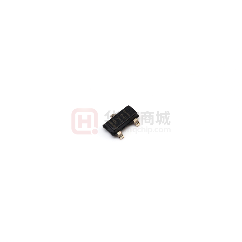
PYZI
TPS3839G33DBZT
ACTIVE
SOT-23
DBZ
3
250
RoHS & Green
NIPDAUAG
Level-1-260C-UNLIM
-40 to 85
PYZI
TPS3839G33DQNR
ACTIVE
X2SON
DQN
4
3000
RoHS & Green
NIPDAU
Level-1-260C-UNLIM
-40 to 85
ZG
TPS3839G33DQNT
ACTIVE
X2SON
DQN
4
250
RoHS & Green
NIPDAU
Level-1-260C-UNLIM
-40 to 85
ZG
TPS3839K33DBZR
ACTIVE
SOT-23
DBZ
3
3000
RoHS & Green
NIPDAUAG
Level-1-260C-UNLIM
-40 to 85
PYYI
TPS3839K33DBZT
ACTIVE
SOT-23
DBZ
3
250
RoHS & Green
NIPDAUAG
Level-1-260C-UNLIM
-40 to 85
PYYI
TPS3839K33DQNR
ACTIVE
X2SON
DQN
4
3000
RoHS & Green
NIPDAU
Level-1-260C-UNLIM
-40 to 85
ZF
Addendum-Page 2
Samples
�PACKAGE OPTION ADDENDUM
www.ti.com
Orderable Device
10-Dec-2020
Status
(1)
Package Type Package Pins Package
Drawing
Qty
Eco Plan
(2)
Lead finish/
Ball material
MSL Peak Temp
Op Temp (°C)
Device Marking
(3)
(4/5)
(6)
TPS3839K33DQNT
ACTIVE
X2SON
DQN
4
250
RoHS & Green
NIPDAU
Level-1-260C-UNLIM
-40 to 85
ZF
TPS3839K50DBZR
ACTIVE
SOT-23
DBZ
3
3000
RoHS & Green
NIPDAUAG
Level-1-260C-UNLIM
-40 to 85
PYXI
TPS3839K50DBZT
ACTIVE
SOT-23
DBZ
3
250
RoHS & Green
NIPDAUAG
Level-1-260C-UNLIM
-40 to 85
PYXI
TPS3839K50DQNR
ACTIVE
X2SON
DQN
4
3000
RoHS & Green
NIPDAU
Level-1-260C-UNLIM
-40 to 85
ZH
TPS3839K50DQNT
ACTIVE
X2SON
DQN
4
250
RoHS & Green
NIPDAU
Level-1-260C-UNLIM
-40 to 85
ZH
TPS3839L30DBZR
ACTIVE
SOT-23
DBZ
3
3000
RoHS & Green
NIPDAUAG
Level-1-260C-UNLIM
-40 to 85
PYWI
TPS3839L30DBZT
ACTIVE
SOT-23
DBZ
3
250
RoHS & Green
NIPDAUAG
Level-1-260C-UNLIM
-40 to 85
PYWI
TPS3839L30DQNR
ACTIVE
X2SON
DQN
4
3000
RoHS & Green
NIPDAU
Level-1-260C-UNLIM
-40 to 85
ZI
TPS3839L30DQNT
ACTIVE
X2SON
DQN
4
250
RoHS & Green
NIPDAU
Level-1-260C-UNLIM
-40 to 85
ZI
(1)
The marketing status values are defined as follows:
ACTIVE: Product device recommended for new designs.
LIFEBUY: TI has announced that the device will be discontinued, and a lifetime-buy period is in effect.
NRND: Not recommended for new designs. Device is in production to support existing customers, but TI does not recommend using this part in a new design.
PREVIEW: Device has been announced but is not in production. Samples may or may not be available.
OBSOLETE: TI has discontinued the production of the device.
(2)
RoHS: TI defines "RoHS" to mean semiconductor products that are compliant with the current EU RoHS requirements for all 10 RoHS substances, including the requirement that RoHS substance
do not exceed 0.1% by weight in homogeneous materials. Where designed to be soldered at high temperatures, "RoHS" products are suitable for use in specified lead-free processes. TI may
reference these types of products as "Pb-Free".
RoHS Exempt: TI defines "RoHS Exempt" to mean products that contain lead but are compliant with EU RoHS pursuant to a specific EU RoHS exemption.
Green: TI defines "Green" to mean the content of Chlorine (Cl) and Bromine (Br) based flame retardants meet JS709B low halogen requirements of


 工商网监
湘ICP备2023018690号
工商网监
湘ICP备2023018690号

