User's Guide
SLVU341 – October 2009
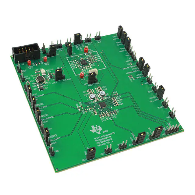
Evaluation Module for TPS386000 and TPS386040
This User's Guide describes the evaluation modules (EVM) for the TPS386000 (TPS386000EVM) and
TPS386040 (TPS386040 EVM). The EVM contains evaluation and reference circuitry for the TPS386000
and TPS386040. TPS386000 and TPS386040 are quad supervisors with reset and sequence capabilities.
1
2
3
4
5
6
7
8
Contents
Description ................................................................................................................... 2
1.1
Features ............................................................................................................. 2
Schematic .................................................................................................................... 3
General Use and Description .............................................................................................. 4
3.1
EVM On-Board Jumper Default Installation .................................................................... 5
3.2
EVM Test Points, Indicators and Switches ..................................................................... 5
3.3
EVM Input/Output Connectors and Test Jumpers ............................................................. 5
Description ................................................................................................................... 7
4.1
General Usage ..................................................................................................... 7
4.2
On EVM Supervisor/Sequencer .................................................................................. 7
4.3
Watch Dog Timer Function ....................................................................................... 9
Test Setup .................................................................................................................. 10
TPS65055 EVM GUI ...................................................................................................... 10
6.1
TPS65055 EVM GUI Installation ............................................................................... 10
7 EVM Assembly Drawings and Layout Guidelines .................................................................. 11
7.1
PCB Drawings .................................................................................................... 11
7.2
Layouts Guidelines ............................................................................................... 15
Bill of Materials ............................................................................................................. 16
List of Figures
1
Typical TPS386000/40EVM Power-on Sequence ...................................................................... 2
2
TPS386000/40 EVM Schematic (TPS386000/40) ...................................................................... 4
3
TPS386000/40 EVM Schematic (TPS65055 Local Power Supply) .................................................. 4
4
Typical TPS386000/40EVM Test Setup ................................................................................ 10
5
Top Side Layout/Routing ................................................................................................. 12
6
Top Side Layout/Routing ................................................................................................. 13
7
Top Side Layout/Routing ................................................................................................. 14
8
Bottom Side Placement/Routing ......................................................................................... 14
List of Tables
1
EVM Default Jumper Installation .......................................................................................... 5
2
EVM Test Points, Indicators and Switches .............................................................................. 5
3
EVM Input/Output Connectors
5
4
EVM Jumpers
6
5
6
............................................................................................
...............................................................................................................
Local Rail Nominal Output Voltages ......................................................................................
TPS386000/40EVM Bill of Materials ...................................................................................
SLVU341 – October 2009
Submit Documentation Feedback
Evaluation Module for TPS386000 and TPS386040
Copyright © 2009, Texas Instruments Incorporated
7
16
1
�Description
1
www.ti.com
Description
The TPS386000/40EVM provides the capabilities needed for supervising and sequencing four power
supplies including one negative power supply. The EVM also provides an I2C interface for use with the TI
USB-GPIO adapter.
The TPS386000/40 interfaces with the TPS65055 providing a sequenced power on and supervised setup
to demonstrate a typical application as shown in Figure 1.
TPS 65055
DCDC 2
LDO 1
LDO 2
LDO 3
DCDC 1
VLDO 3
SENSE 2
RESET 2
SENSE 1
SVS 2
SVS_EN1
RESET 3
SVS 3
SVS_EN2
SENSE 3
EN
VLDO2
RESET 4
EN
VLDO1
SVS 4
VDCDC2
VDCDC1
SENSE 4
EN
SVS_EN4
EN
SVS_EN3
VIN
RESET 1
SVS 1
TPS3860x0
Figure 1. Typical TPS386000/40EVM Power-on Sequence
The TPS386000/40EVM can also be configured to sequence and supervise an external power supply
system including one negative power supply.
1.1
Features
•
•
2
General features
– On board local power supply used to demonstrate the sequencing and supervision capabilities of
the TPS3860x0.
– Single 5V EVM supply input
– 4 rail on EVM and external sequencing
– 4 analog supervisors including one negative supervisor
– USB interface for communication with on board TPS65055 power management unit.
Orderable options
– TPS386000EVM 4 channel supervisor/sequencer with open drain RESET outputs
– TPS386040EVM 4 channel supervisor/sequencer with push-pull RESET outputs
Evaluation Module for TPS386000 and TPS386040
Copyright © 2009, Texas Instruments Incorporated
SLVU341 – October 2009
Submit Documentation Feedback
�Schematic
www.ti.com
Schematic
2
1
2
2
2
2
2
1
1
1
1
1
2
Figure 2. TPS386000/40 EVM Schematic (TPS386000/40)
SLVU341 – October 2009
Submit Documentation Feedback
Evaluation Module for TPS386000 and TPS386040
Copyright © 2009, Texas Instruments Incorporated
3
�General Use and Description
www.ti.com
Figure 3. TPS386000/40 EVM Schematic (TPS65055 Local Power Supply)
3
4
General Use and Description
Evaluation Module for TPS386000 and TPS386040
Copyright © 2009, Texas Instruments Incorporated
SLVU341 – October 2009
Submit Documentation Feedback
�General Use and Description
www.ti.com
3.1
EVM On-Board Jumper Default Installation
As ordered, the EVM should have 18 jumpers installed in the following locations.
Table 1. EVM Default Jumper Installation
3.2
Shunt Reference Designator
Shunt Pin Position
J2, J5-J8, J11, J20, J22, J24, J28, J31, J34, JP2, JP5
Between pins 1 and 2
J4, JP1, JP3, JP4
Between pins 2 and 3
EVM Test Points, Indicators and Switches
Table 2. EVM Test Points, Indicators and Switches
3.3
TP/LED/SW
Label
S1
MR
Description
D2 (GRN)
LWDT ON
TP1 (RED)
VREF
TP2 (RED)
MR
TP3 (RED)
SCLK
Serial clock input to TPS65055 from USB-GPIO adapter.
TP4 (RED)
SDAT
Serial data input-output to TPS65055 from USB-GPIO adapter.
Master reset input switch for TPS3860x0. Use this switch to reset the WDO pin and force local
resequence.
Indicates when the local watch dog timer is operational.
TPS3860x0 VREF output nominally 1.2V
TPS3860x0 MR (master reset) input.
EVM Input/Output Connectors and Test Jumpers
Table 3. EVM Input/Output Connectors
Connector
Description
J14
EVM 5V input voltage (VIN). Use with GND at J16 and with JP1 set to the VIN position.
J16
EVM input GND used with J14 (VIN).
J3
Negative supply input used with J3 (GND). Set J4 shunt to the NEGVDC SNS4H position to monitor negative
supplies using SENSE4H.
J1
GND input used with J3 (NEGVDC).
J13
TPS65055 DCDC1 output voltage (VDCDC1) which is nominally 2.1VDC.
J15
GND output used with J13 (VDCDC1).
J17
TPS65055 DCDC2 output voltage (VDCDC2) which is nominally 1.0VDC.
J18
GND output used with J17 (VDCDC2).
J19
TPS65055 LDO1 output voltage (VLDO1) which is nominally 1.2VDC.
J21
GND output used with J19 (VLDO1).
J23
TPS65055 LDO2 output voltage (VLDO2) which is nominally 1.8VDC.
J25
GND output used with J23 (VLDO2).
J27
TPS65055 LDO3 output voltage (VLDO3) which is nominally 2.8VDC.
J29
GND output used with J27 (VLDO3).
J30
TPS65055 LDO4 output voltage (VLDO4) which is nominally 1.3VDC.
J32
GND output used with J30 (VLDO4).
J33
Used with the USB-GPIO adapter for communication with the TPS65055 using the TPS65055 GUI. The USB-GPIO
adapter can also provide 3.3V to the EVM (derived from the PC on which the GUI is operating) when JP1 is in the
3.3V position.
J12
Local watch dog timer reset (RST LWDT). Use this when J11 is set to the LWDT position when testing the watch
dog timer function. When a shunt is installed on J12 the local watch dog timer will reset causing the TPS3860x0
WDO signal to go low after timeout.
J10
External watch dog timer input terminal. Use this input when J11 is set to the EXT WDT position.
J9
TPS3860x0 WDO pin output.
SLVU341 – October 2009
Submit Documentation Feedback
Evaluation Module for TPS386000 and TPS386040
Copyright © 2009, Texas Instruments Incorporated
5
�General Use and Description
www.ti.com
Table 4. EVM Jumpers
Jumper
JP1
6
Description
EVM input voltage select jumper. Install shunt between pins 2 and 3 (5V) for normal external 5V power supply input
from J14 and J16. Install shunt between pins 1 and 2 (3.3V) when using the USB-GPIO adapter to communicate
with the TPS65055 through J33. USB power from the USB-GPIO adapter is nominally 3.3VDC.
J2
VIN source for TPS3860x0. Install shunt for normal operation.
J22
VIN source for TPS65055 LDO1, LDO2, LDO3, LDO4. Install shunt for normal operation.
J11
Watch Dog Input Select. Place shunt in the LWDT position for the local watch dog timer and place the shunt in the
EXT WDT position for the external watch dog timer source via J10.
J31
RESET1 output from TPS3860x0. Install shunt between pins 1 and 2 (RESET1) for local LDO3 enable (EN_LDO3)
or remove shunt and connect RESET1 to external power supply enable for system operation. Install shunt between
pins 2 and 3 to always enable LDO3.
J28
RESET2 output from TPS3860x0. Install shunt between pins 1 and 2 (RESET2) for local LDO2 enable (EN_LDO2)
or remove shunt and connect RESET2 to external power supply enable for system operation. Install shunt between
pins 2 and 3 to always enable LDO2.
J24
RESET3 output from TPS3860x0. Install shunt between pins 1 and 2 (RESET3) for local LDO1 enable (EN_LDO1)
or remove shunt and connect RESET3 to external power supply enable for system operation. Install shunt between
pins 2 and 3 to always enable LDO1.
J20
RESET4 output from TPS3860x0. Install shunt between pins 1 and 2 (RESET4) for local DCDC2 enable
(EN_DCDC2) or remove shunt and connect RESET4 to external power supply enable for system operation. Install
shunt between pins 2 and 3 to always enable DCDC2.
J8
SENSE1 input to TPS650x0 derived from TPS65055 LDO2. Install shunt for normal local operation or remove shunt
and connect SNS1 to external supply output for system operation.
J7
SENSE2 input to TPS650x0 derived from TPS65055 LDO1. Install shunt for normal local operation or remove shunt
and connect SNS2 to external supply output for system operation.
J6
SENSE3 input to TPS650x0 derived from TPS65055 DCDC2. Install shunt for normal local operation or remove
shunt and connect SNS3 to external supply output for system operation.
J5
SENSE4L input to TPS650x0 derived from TPS65055 DCDC1. Install shunt for normal local operation or remove
shunt and connect SNS4 to external supply output for system operation.
J4
SENSE4H input to TPS650x0 derived from TPS65055 DCDC1. Install shunt between pins 2 and 3 (VDCDC1
SNS4H) for normal local operation or install shunt between pins 1 and 2 (NEGVDC SNS4H) to monitor negative
external power supply using J3 and J1.
J34
Enable input for local TPS65055 LDO4. Install shunt for normal operation.
JP2
TPS65055 DCDC1 enable. Install shunt between pins 1 and 2 (HIGH) to enable DCDC1 and between pins 2 and 3
(GND) to disable DCDC1.
JP5
Used to select TPS65055 DCDC2 output voltage. Refer to the TPS65055 datasheet for more detail.
JP4
Used with JP3 to select TPS65055 LDO1-LDO4 output voltage. Refer to the TPS65055 datasheet for more detail.
JP3
Used with JP4 to select TPS65055 LDO1-LDO4 output voltage. Refer to the TPS65055 datasheet for more detail.
J26
TPS65055 control signal input. Refer to TPS65055 datasheet for control signal explanation.
Evaluation Module for TPS386000 and TPS386040
Copyright © 2009, Texas Instruments Incorporated
SLVU341 – October 2009
Submit Documentation Feedback
�Description
www.ti.com
4
Description
The following paragraphs describe the functionality and operation of the TPS386000/40 EVM.
4.1
4.1.1
General Usage
Input Power
The 5VDC EVM input power is provided through J14/J16 terminals. Ensure that the correct polarity is
provided and that this input voltage does not exceed 6.0VDC. The normal operating current for the
TPS386000/40EVM will be less than 50mA when there is no load on the TPS65055 outputs. 3.3VDC EVM
input power can also be furnished at the J33 (I2C) connector through the USB-GPIO adapter when using
the TPS65055 GUI. In this case, 5VDC EVM input power is not required.
4.1.2
I2C Interface
An I2C interface to the TPS65055 is provided at J33. The TPS65055 internal registers and output voltages
can be modified using a GUI.
4.2
On EVM Supervisor/Sequencer
The TPS386000/40 and TPS65055 are configured to provide a power-on sequence as shown in Figure 1.
When power is applied to the EVM, VDCDC1 rises to approximately 2.1VDC causing RESET4 to enable
DCDC2. VDCDC2 rises to approximately 1.0VDC causing RESET3 to enable LDO1. VLDO1 rises to
approximately 1.2VDC causing RESET2 to enable LDO2. VLDO2 rises to approximately 1.8VDC causing
RESET1 to enable LDO3. VLDO3 then rises to approximately 2.8V and the sequence is complete.
4.2.1
Local Voltage Rails
The TPS65055 provides DC outputs from 2 switching (DCDC1 and DCDC2) and 4 linear power supplies
(LDO1-LDO4) for sequencing and monitoring. The nominal output voltages are listed in Table 5.
Table 5. Local Rail Nominal Output Voltages
Local Rail
VDCDC1
VDCDC2
VLDO1
VLDO2
VLDO3
VLDO4
Nominal Voltage
2.1V
1.0V
1.2V
1.8V
2.8V
1.3V
SLVU341 – October 2009
Submit Documentation Feedback
Evaluation Module for TPS386000 and TPS386040
Copyright © 2009, Texas Instruments Incorporated
7
�Description
4.2.2
www.ti.com
Supervisor Inputs
The TPS386000/40 supervisor inputs (SENSE1L, SENSE2L, SENSE3L, SENSE4L, and SENSE4H) can
be used to monitor onboard or off board voltages. Jumpers are used to select the analog source. The
default EVM configuration monitors the onboard voltage rails as described above. The SENSE1L-SENS4L
inputs are programmed with a resistor divider which turns on at approximately 75% of the rail nominal
output voltage. The SENS4H input is set below the 400mV threshold by default when using the onboard
power supplies.
The supervisor inputs can also be used to monitor an external power supply source by removing the
associated jumper shunt and connecting the jumper pin to the external source. The SENSE input trip
points can be adjusted by changing the resistor dividers using the following equations:
VITN = 400 mV
æ VCC_target ö
æ RSU
ö
RSU = RSL ´ ç
+1÷
÷ - 1, VCC_target = VITN ´ ç
V
R
è
ø
è SL
ø
ITN
Example for EVM SENSE1 input from LDO2
VCC_target = 1.35 V, RSL = 100 kΩ
æ 1.35V
ö
RSU = 100 kΩ ´ ç
- 1÷ = 237.5 kΩ (choose 237 kΩ)
è 0.4V
ø
æ 237kΩ ö
VCC_target = 0.4 V ´ ç
+1÷ = 1.348 V
è 100kΩ ø
Additionally, the SENSE4H input can be used along with VREF to monitor negative voltages applied at
J3/J1. J4 jumper must also be installed to the NEGVDC SNS4H position when monitoring negative
voltages. The onboard resistors have been chosen so that SENSE4H trips with approximately –4.2V at
J3/J1 for a –5VDC nominal power supply. The SENSE4H input trip points can be adjusted by changing
the resistor dividers using the following equations:
VREF = 1.2 V, VITP = 400 mV
RS42L = RS42H ´
VITP - VCC42_target
VREF - VITP
VCC42_target = VITP -
RS42L
´ (VREF - VITP )
RS42H
Example for EVM SENSE4H input from NEGVDC
VCC42_target = - 4.2 V, RS42H = 49.9 kΩ
é 0.4 V - (-4.2 ) V ù
RS42L = 49.9 kΩ ´ ê
ú = 286.9 kΩ
ëê 1.2 V - 0.4 V ûú
VCC42_target = 0.4V -
(choose 287 kΩ )
287 kΩ
´ (1.2V- 0.4V) = 4.201 V
49.9 kΩ
The EVM includes a PCB footprint for a small filter capacitor on each of the SENSE inputs for use with
noisy external sources.
8
Evaluation Module for TPS386000 and TPS386040
Copyright © 2009, Texas Instruments Incorporated
SLVU341 – October 2009
Submit Documentation Feedback
�Description
www.ti.com
4.2.3
RESET Outputs
The TPS386000/40 RESET outputs are used on the EVM to enable the associated power supplies. The
TPS386000 has open drain outputs and are pulled up by R3-R6 pullup resistors by default on the
TPS386000EVM. The TPS386040 has push-pull outputs and R3-R6 are not installed on the
TPS386040EVM.
Jumpers allow the RESET pins to be connected to an external power supply enable for use with a user
system.
4.2.4
Timing Delay on CT Pins
Delay from SENSE input to output RESET can be adjusted with the value at the CT1-CT4 pins. Use the
following equations to adjust the delay from the nominal 1.3mS EVM value.
VCT = 1.24V, ICT = 300 nA, TDELAY = 1.4 ms
CCT =
ICT
VCT
´
(TDELAY
- 0.5 ms )
Example for EVM CT pins with a desired TDELAY = 1.4 ms
CCT =
TDELAY
4.3
300 nA
´ (1.4 ms - 0.5 ms) = 218 pF (choose CCT = 220 pF)
1.24 V
1.24 V
= 220 pF ´
+ 0.5 ms = 1.41 ms
300 nA
Watch Dog Timer Function
The TPS386000/40 contains a watch dog timer (WDT) and the EVM contains a local WDT (LWDT) as well
as a provision for an external WDT connection. LWDT provides a pulse approximately every 140ms to the
TPS386000/40 WDI pin when configured by J11. LED D2 indicates when the LWDT is active.
The TPS386000/40 WDT function can be tested in the LWDT mode by holding LWDT in reset by placing
a shunt on J12 (RST LWDT). When a shunt is installed on J12, the WDO output on J9 will go to logic low
after approximately 600ms. WDO can be reset to logic high by pressing the S1 push-button switch to reset
the TPS386000/40.
A system WDT can also be provided externally through J10 when J11 is set to the EXT WDT position.
SLVU341 – October 2009
Submit Documentation Feedback
Evaluation Module for TPS386000 and TPS386040
Copyright © 2009, Texas Instruments Incorporated
9
�Test Setup
5
www.ti.com
Test Setup
Figure 4 shows a typical test setup for TPS386000/40EVM.
USB CABLE
5V
Power
Supply
USB-GPIO
Adapter
RIBBON
CABLE
GND VIN
I/O CONNECTORS AND JUMPERS
PC with GUI
GND
S1
U1
TPS386000
or
TPS386040
NEGVDC
TPS386000/40EVM
U4
TPS65055
J1
MR
J3
I2C
-5V
Power
Supply
I/O CONNECTORS AND JUMPERS
J14
J16
J33
I/O CONNECTORS AND JUMPERS
Figure 4. Typical TPS386000/40EVM Test Setup
6
TPS65055 EVM GUI
6.1
TPS65055 EVM GUI Installation
The TPS65055 EVM Software provides a software interface for the TPS65055 EVM boards. Use this
software to change the TPS65055 IC registers via the USB Interface Adapter. Navigate to the following
link to download the software:
http://focus.ti.com/docs/toolsw/folders/print/tps65055evm-sw.html
6.1.1
Software Requirements
Microsoft Windows 2000 or Newer Operating System
Microsoft .Net Framework 2.0
NOTE: It is advised to install this component independently. This EVM software will attempt to install it
if it's not already installed, but it might require a restart of your system.
• Microsoft Internet Explorer 6
• This is required for receiving automatic updates to the EVM software.
•
•
•
6.1.2
•
•
10
Personal Computer with USB port
USB Interface Adapter
Evaluation Module for TPS386000 and TPS386040
Copyright © 2009, Texas Instruments Incorporated
SLVU341 – October 2009
Submit Documentation Feedback
�7 EVM Assembly Drawings and Layout Guidelines
www.ti.com
7
7 EVM Assembly Drawings and Layout Guidelines
7.1
PCB Drawings
The following figures show component placement and layout.
Figure 5. Top Side Layout/Routing
SLVU341 – October 2009
Submit Documentation Feedback
Evaluation Module for TPS386000 and TPS386040
Copyright © 2009, Texas Instruments Incorporated
11
�7 EVM Assembly Drawings and Layout Guidelines
www.ti.com
Figure 6. Top Side Layout/Routing
12
Evaluation Module for TPS386000 and TPS386040
Copyright © 2009, Texas Instruments Incorporated
SLVU341 – October 2009
Submit Documentation Feedback
�www.ti.com
7 EVM Assembly Drawings and Layout Guidelines
Figure 7. Top Side Layout/Routing
SLVU341 – October 2009
Submit Documentation Feedback
Evaluation Module for TPS386000 and TPS386040
Copyright © 2009, Texas Instruments Incorporated
13
�7 EVM Assembly Drawings and Layout Guidelines
www.ti.com
Figure 8. Bottom Side Placement/Routing
14
Evaluation Module for TPS386000 and TPS386040
Copyright © 2009, Texas Instruments Incorporated
SLVU341 – October 2009
Submit Documentation Feedback
�www.ti.com
7.2
7 EVM Assembly Drawings and Layout Guidelines
Layouts Guidelines
Thermal pad
The thermal pad provides a thermal and mechanical interface between the device and the printed circuit
board (PCB). Connect the exposed thermal pad of the PCB to the device VSS pins and provide at least a
3 x 3 pattern of PCB vias to connect the thermal pad and GND pin to the circuit ground on other PCB
layers.
Supply voltage decoupling
Provide power supply pin bypass to the device as follows:
• 0.1µF, X7R ceramic at pin 15 (VCC)
• 1nF, X7R ceramic at pins 6-10 (SENSE1, SENSE2, SENSE3, SENSE4L, SENSE4H) while not
absolutely required can provide noise filtering in noisy power supply systems.
SLVU341 – October 2009
Submit Documentation Feedback
Evaluation Module for TPS386000 and TPS386040
Copyright © 2009, Texas Instruments Incorporated
15
�Bill of Materials
8
www.ti.com
Bill of Materials
Table 6. TPS386000/40EVM Bill of Materials
EVM COUNT
RefDes
Value
Descripotion
Size
Part Number
MFR
3
C1, C13, C25
0.1 µF
Capacitor, Ceramic, X7R, 16V, 10%
0603
Std
Std
2
2
C14, C16
0.01 µF
Capacitor, Ceramic, X7R, 16V, 10%
0603
Std
Std
1
1
C15
0.33 µF
Capacitor, Ceramic, X7R, 16V, 10%
0603
Std
Std
6
6
C18, C19,
C20, C21,
C22, C23
10 µF
Capacitor, Ceramic, 10V, X5R, 10%
0805
GRM21BR61A106KE19L
Murata
5
5
C2, C9, C10,
C11, C12
220 pF
Capacitor, Ceramic, COG, 50V, 5%
0603
Std
Std
2
2
C24, C27
4.7 µF
Capacitor, Ceramic, 10V, X5R, 10%
0805
GRM219R61A475KE19D
Murata
5
5
C26, C28,
2.2 µF
C29, C30, C31
Capacitor, Ceramic, 10V, X5R, 10%
0603
GRM188R61A225KE34D
Murata
0
0
C3, C4, C5,
C6, C7
1 nF
Capacitor, Ceramic, X7R, 16V, 10%
0603
Std
Std
2
2
C8, C17
1.0 µF
Capacitor, Ceramic, 25V, X5R, 10%
0603
GRM188R61E105KA12D
Murata
1
1
D1
1N4148W
Diode, Signal, 300-mA, 75-V, 350-mW
SOD-123
1N4148W
Diodes
1
1
D2
SML-LX2832GC-TR
Diode. LED, Green, 2.1-V, 25-mcd,SM
1210
SML-LX2832GC-TR
Lumex
26
26
J1, J2, J3, J5,
J6, J7, J8, J9,
J10, J12, J13,
J14, J15, J16,
J17, J18, J19,
J21, J22, J23,
J25, J27, J29,
J30, J32, J34
PEC02SAAN
Header, Male 2-pin, 100mil spacing,
0.100 inch × 2
PEC02SAAN
Sullins
1
1
J26
PEC04SAAN
Header, Male 4-pin, 100mil spacing,
0.100 inch × 4
PEC04SAAN
Sullins
1
1
J33
N2510-6002-RB
Connector, Male Straight 2x5 pin, 100mil
spacing, 4 Wall
0.338 × 0.788 inch
N2510-6002-RB
3M
6
6
J4, J11, J20,
J24, J28, J31
PEC03SAAN
Header, Male 3-pin, 100mil spacing,
0.100 inch × 3
PEC03SAAN
Sullins
5
5
JP1, JP2, JP3,
JP4, JP5
PEC03SAAN
Header, 3-pin, 100mil spacing
0.100 inch × 3
PEC03SAAN
Sullins
2
2
L1, L2
2.2 µH
Inductor, SMT, 2.5A, 70milliohm
0.153 × 0.153 inch
LPS4018-222ML
Coilcraft
2
2
R1, R14
49.9k
Resistor, Chip, 1/16W, 1%
0603
Std
Std
1
1
R11
127k
Resistor, Chip, 1/16W, 1%
0603
Std
Std
1
1
R12
237k
Resistor, Chip, 1/16W, 1%
0603
Std
Std
TPS386040
TPS386000
3
16
Evaluation Module for TPS386000 and TPS386040
SLVU341 – October 2009
Submit Documentation Feedback
Copyright © 2009, Texas Instruments Incorporated
�Bill of Materials
www.ti.com
Table 6. TPS386000/40EVM Bill of Materials (continued)
EVM COUNT
RefDes
Value
Descripotion
Size
Part Number
MFR
1
R19
1k
Resistor, Chip, 1/16W, 1%
0603
Std
Std
1
R2
287k
Resistor, Chip, 1/16W, 1%
0603
Std
Std
1
1
R20
10
Resistor, Chip, 1/16W, 1%
0603
Std
Std
1
1
R22
100
Resistor, Chip, 1/16W, 1%
0603
Std
Std
1
1
R23
619k
Resistor, Chip, 1/16W, 1%
0805
Std
Std
1
1
R24
665
Resistor, Chip, 1/16W, 1%
0805
Std
Std
1
1
R25
0
Resistor, Chip, 1/16W, 1%
0603
Std
Std
1
1
R26
499
Resistor, Chip, 1/16W, 1%
0805
Std
Std
0
4
R3, R4, R5, R6 10k
Resistor, Chip, 1/16W, 1%
0603
Std
Std
1
1
R21
10k
Resistor, Chip, 1/16W, 1%
0603
Std
Std
1
1
R32
357k
Resistor, Chip, 1/16W, 1%
0603
Std
Std
2
2
R36, R37
4.75k
Resistor, Chip, 1/16W, 1%
0603
Std
Std
15
15
R10,
R15,
R17,
R27,
R29,
R31,
R34,
R13,
100k
R16,
R18,
R28,
R30,
R33,
R35, R38
Resistor, Chip, 1/16W, 1%
0603
Std
Std
0
1
R7
100k
Resistor, Chip, 1/16W, 1%
0603
Std
Std
1
1
R8
576k
Resistor, Chip, 1/16W, 1%
0603
Std
Std
1
1
R9
301k
Resistor, Chip, 1/16W, 1%
0603
Std
Std
1
1
S1
EVQ-PJA04Q
Switch, 1P1T, PB Momentary, 50-mA
0.24 × 0.14 inch
EVQ-PJA04Q
Panasonic
2
2
TP3, TP4
5000
Test Point, Red, Thru Hole Color Keyed
0.100 × 0.100 inch
5000
Keystone
2
2
TP1, TP2
5005
Test Point, Red, Thru Hole Compact
Style
0.125 × 0.125 inch
5005
Keystone
0
1
U1
TPS386000RGP
IC, Quad Supply Voltage Supervisors,
Open Drain RESET
TPS386000RGP
TI
1
0
U1
TPS386040RGP
IC, Quad Supply Voltage Supervisors,
Push-Pull RESET
TPS386040RGP
TI
1
1
U2
TLC555CD
IC, Timer, Low-Power CMOS
SO8
TLC555CD
TI
1
1
U3
SN74LVC1G04DBV
IC, Single Inverter
SOT23-5
SN74LVC1G04DBV
TI
1
1
U4
TPS65055RSM
IC, 2.25MHz, Two Step Down DC to DC
Converters with PWM and PFM features,
4 LDOs
TPS65055RSM
TI
18
18
–
929950-00
3M
TPS386040
TPS386000
1
1
Shunt, Black
SLVU341 – October 2009
Submit Documentation Feedback
100-mil
Evaluation Module for TPS386000 and TPS386040
Copyright © 2009, Texas Instruments Incorporated
17
�Bill of Materials
www.ti.com
Table 6. TPS386000/40EVM Bill of Materials (continued)
EVM COUNT
RefDes
TPS386040
TPS386000
4
4
1
1
18
Value
Descripotion
SJ-5003
–
Part Number
MFR
BUMPON HEMISPHERE .44X.20 BLACK
SJ-5003
3M
PCB, 4.2 In × 3.7 In × 0.062 In
HPA428
Any
Evaluation Module for TPS386000 and TPS386040
Size
SLVU341 – October 2009
Submit Documentation Feedback
Copyright © 2009, Texas Instruments Incorporated
�EVALUATION BOARD/KIT IMPORTANT NOTICE
Texas Instruments (TI) provides the enclosed product(s) under the following conditions:
This evaluation board/kit is intended for use for ENGINEERING DEVELOPMENT, DEMONSTRATION, OR EVALUATION PURPOSES
ONLY and is not considered by TI to be a finished end-product fit for general consumer use. Persons handling the product(s) must have
electronics training and observe good engineering practice standards. As such, the goods being provided are not intended to be complete
in terms of required design-, marketing-, and/or manufacturing-related protective considerations, including product safety and environmental
measures typically found in end products that incorporate such semiconductor components or circuit boards. This evaluation board/kit does
not fall within the scope of the European Union directives regarding electromagnetic compatibility, restricted substances (RoHS), recycling
(WEEE), FCC, CE or UL, and therefore may not meet the technical requirements of these directives or other related directives.
Should this evaluation board/kit not meet the specifications indicated in the User’s Guide, the board/kit may be returned within 30 days from
the date of delivery for a full refund. THE FOREGOING WARRANTY IS THE EXCLUSIVE WARRANTY MADE BY SELLER TO BUYER
AND IS IN LIEU OF ALL OTHER WARRANTIES, EXPRESSED, IMPLIED, OR STATUTORY, INCLUDING ANY WARRANTY OF
MERCHANTABILITY OR FITNESS FOR ANY PARTICULAR PURPOSE.
The user assumes all responsibility and liability for proper and safe handling of the goods. Further, the user indemnifies TI from all claims
arising from the handling or use of the goods. Due to the open construction of the product, it is the user’s responsibility to take any and all
appropriate precautions with regard to electrostatic discharge.
EXCEPT TO THE EXTENT OF THE INDEMNITY SET FORTH ABOVE, NEITHER PARTY SHALL BE LIABLE TO THE OTHER FOR ANY
INDIRECT, SPECIAL, INCIDENTAL, OR CONSEQUENTIAL DAMAGES.
TI currently deals with a variety of customers for products, and therefore our arrangement with the user is not exclusive.
TI assumes no liability for applications assistance, customer product design, software performance, or infringement of patents or
services described herein.
Please read the User’s Guide and, specifically, the Warnings and Restrictions notice in the User’s Guide prior to handling the product. This
notice contains important safety information about temperatures and voltages. For additional information on TI’s environmental and/or
safety programs, please contact the TI application engineer or visit www.ti.com/esh.
No license is granted under any patent right or other intellectual property right of TI covering or relating to any machine, process, or
combination in which such TI products or services might be or are used.
FCC Warning
This evaluation board/kit is intended for use for ENGINEERING DEVELOPMENT, DEMONSTRATION, OR EVALUATION PURPOSES
ONLY and is not considered by TI to be a finished end-product fit for general consumer use. It generates, uses, and can radiate radio
frequency energy and has not been tested for compliance with the limits of computing devices pursuant to part 15 of FCC rules, which are
designed to provide reasonable protection against radio frequency interference. Operation of this equipment in other environments may
cause interference with radio communications, in which case the user at his own expense will be required to take whatever measures may
be required to correct this interference.
EVM WARNINGS AND RESTRICTIONS
It is important to operate this EVM within the input voltage range of 0 V to 7 V and the output voltage range of 0 V to 7 V.
Exceeding the specified input range may cause unexpected operation and/or irreversible damage to the EVM. If there are questions
concerning the input range, please contact a TI field representative prior to connecting the input power.
Applying loads outside of the specified output range may result in unintended operation and/or possible permanent damage to the EVM.
Please consult the EVM User's Guide prior to connecting any load to the EVM output. If there is uncertainty as to the load specification,
please contact a TI field representative.
During normal operation, some circuit components may have case temperatures greater than +85°C. The EVM is designed to operate
properly with certain components above +85°C as long as the input and output ranges are maintained. These components include but are
not limited to linear regulators, switching transistors, pass transistors, and current sense resistors. These types of devices can be identified
using the EVM schematic located in the EVM User's Guide. When placing measurement probes near these devices during operation,
please be aware that these devices may be very warm to the touch.
Mailing Address: Texas Instruments, Post Office Box 655303, Dallas, Texas 75265
Copyright © 2009, Texas Instruments Incorporated
�IMPORTANT NOTICE
Texas Instruments Incorporated and its subsidiaries (TI) reserve the right to make corrections, modifications, enhancements, improvements,
and other changes to its products and services at any time and to discontinue any product or service without notice. Customers should
obtain the latest relevant information before placing orders and should verify that such information is current and complete. All products are
sold subject to TI’s terms and conditions of sale supplied at the time of order acknowledgment.
TI warrants performance of its hardware products to the specifications applicable at the time of sale in accordance with TI’s standard
warranty. Testing and other quality control techniques are used to the extent TI deems necessary to support this warranty. Except where
mandated by government requirements, testing of all parameters of each product is not necessarily performed.
TI assumes no liability for applications assistance or customer product design. Customers are responsible for their products and
applications using TI components. To minimize the risks associated with customer products and applications, customers should provide
adequate design and operating safeguards.
TI does not warrant or represent that any license, either express or implied, is granted under any TI patent right, copyright, mask work right,
or other TI intellectual property right relating to any combination, machine, or process in which TI products or services are used. Information
published by TI regarding third-party products or services does not constitute a license from TI to use such products or services or a
warranty or endorsement thereof. Use of such information may require a license from a third party under the patents or other intellectual
property of the third party, or a license from TI under the patents or other intellectual property of TI.
Reproduction of TI information in TI data books or data sheets is permissible only if reproduction is without alteration and is accompanied
by all associated warranties, conditions, limitations, and notices. Reproduction of this information with alteration is an unfair and deceptive
business practice. TI is not responsible or liable for such altered documentation. Information of third parties may be subject to additional
restrictions.
Resale of TI products or services with statements different from or beyond the parameters stated by TI for that product or service voids all
express and any implied warranties for the associated TI product or service and is an unfair and deceptive business practice. TI is not
responsible or liable for any such statements.
TI products are not authorized for use in safety-critical applications (such as life support) where a failure of the TI product would reasonably
be expected to cause severe personal injury or death, unless officers of the parties have executed an agreement specifically governing
such use. Buyers represent that they have all necessary expertise in the safety and regulatory ramifications of their applications, and
acknowledge and agree that they are solely responsible for all legal, regulatory and safety-related requirements concerning their products
and any use of TI products in such safety-critical applications, notwithstanding any applications-related information or support that may be
provided by TI. Further, Buyers must fully indemnify TI and its representatives against any damages arising out of the use of TI products in
such safety-critical applications.
TI products are neither designed nor intended for use in military/aerospace applications or environments unless the TI products are
specifically designated by TI as military-grade or "enhanced plastic." Only products designated by TI as military-grade meet military
specifications. Buyers acknowledge and agree that any such use of TI products which TI has not designated as military-grade is solely at
the Buyer's risk, and that they are solely responsible for compliance with all legal and regulatory requirements in connection with such use.
TI products are neither designed nor intended for use in automotive applications or environments unless the specific TI products are
designated by TI as compliant with ISO/TS 16949 requirements. Buyers acknowledge and agree that, if they use any non-designated
products in automotive applications, TI will not be responsible for any failure to meet such requirements.
Following are URLs where you can obtain information on other Texas Instruments products and application solutions:
Products
Amplifiers
Data Converters
DLP® Products
DSP
Clocks and Timers
Interface
Logic
Power Mgmt
Microcontrollers
RFID
RF/IF and ZigBee® Solutions
amplifier.ti.com
dataconverter.ti.com
www.dlp.com
dsp.ti.com
www.ti.com/clocks
interface.ti.com
logic.ti.com
power.ti.com
microcontroller.ti.com
www.ti-rfid.com
www.ti.com/lprf
Applications
Audio
Automotive
Broadband
Digital Control
Medical
Military
Optical Networking
Security
Telephony
Video & Imaging
Wireless
www.ti.com/audio
www.ti.com/automotive
www.ti.com/broadband
www.ti.com/digitalcontrol
www.ti.com/medical
www.ti.com/military
www.ti.com/opticalnetwork
www.ti.com/security
www.ti.com/telephony
www.ti.com/video
www.ti.com/wireless
Mailing Address: Texas Instruments, Post Office Box 655303, Dallas, Texas 75265
Copyright © 2009, Texas Instruments Incorporated
�