User's Guide
SLVU524A – August 2011 – Revised September 2011
TPS389xA-xP-EVM047 Evaluation Modules
This user’s guide describes the characteristics and operational use of the TPS389XA-XP-EVM047
Evaluation Module (EVM) for engineering demonstration of the TPS3897A and TPS3896P supervisors
(TPS3897A-6P-EVM047), the TPS3897P and TPS3896A supervisors (TPS3897P-6A-EVM047), the
TPS3898A and TPS3895P supervisors (TPS3898A-5P-EVM047), or the TPS3898P and TPS3895A
supervisors (TPS3898P-5AEVM047). These EVMs are fully assembled and tested platforms for evaluating
the performance of the TPS389xA-xP family of supervisory circuits. Any one EVM can be manually
modified to easily accommodate alternative supervisor ICs of this same family. This TPS389XA-XP family
are adjustable supervisors in an ultra small package, that can monitor voltages greater than the 500 mV
sense voltage, whose accuracy is better than 1%. This user’s guide includes setup instructions,
schematic, bill of materials (BOM), layout, and test results for a typical SVS circuit on the EVM
1
2
3
4
5
6
Contents
Introduction .................................................................................................................. 2
1.1
Features ............................................................................................................. 2
1.2
EVM Interface Information and Orderable Options (Dependent on Customer Demand and
Availability) .......................................................................................................... 2
Schematic .................................................................................................................... 3
I/O Description, Threshold and Delay Calculations, and Setup ....................................................... 4
3.1
EVM Input/Output Connectors and Test Jumpers ............................................................. 4
3.2
CT and Output Delay Time ....................................................................................... 4
3.3
SVS SENSE Voltage Threshold: Programming the Threshold Voltage .................................... 4
3.4
........................................................................................................................ 5
Operation ..................................................................................................................... 5
4.1
Operation Description ............................................................................................. 5
4.2
Test Results ........................................................................................................ 5
Board Layout ................................................................................................................ 7
Bill of Materials ............................................................................................................. 10
List of Figures
1
TPS389xA-xP-EVM-047 Schematic ...................................................................................... 3
2
Sense_out response (active high) to rising/falling SVS SENSE (TPS3895A) ...................................... 6
3
Sense_out response (active low) to rising/falling SVS SENSE (TPS3898A) ....................................... 6
4
Assembly Layer (Top) ...................................................................................................... 7
5
Top Layer Routing .......................................................................................................... 8
6
Bottom Layer Routing ...................................................................................................... 9
List of Tables
1
SVS Circuit Interface Information based on EVM Orderable.......................................................... 2
2
EVM Input/Output Connectors and Jumpers ............................................................................ 4
3
SVS SENSE Threshold Accuracy and Resistor Divider Selection ................................................... 5
4
EVM Assembly Associated with EVM Orderable...................................................................... 10
5
...............................................................................................................................
SLVU524A – August 2011 – Revised September 2011
Submit Documentation Feedback
TPS389xA-xP-EVM047 Evaluation Modules
Copyright © 2011, Texas Instruments Incorporated
11
1
�Introduction
1
www.ti.com
Introduction
The TPS389xA-xP-EVM047 helps designers evaluate the operation and performance of the TPS389xA-xP
family of single channel supervisors (SVS) available in the ultra small µSon package. Each EVM has two
completely independent SVS circuits each preprogrammed by a resistor divider to monitor a 3.3 V SVS
SENSE rail. Each SVS circuit issues the active Sense_out when the SVS SENSE voltage rises above the
preprogrammed threshold, which in this case is set to 94.5% of the 3.3 V rail (nominally) by the divider
resistors. The Sense_out is inactive when the SVS SENSE falls below the threshold minus hysteresis, or
when the part is disabled. The SVS part itself is capable of monitoring voltage rails greater than 500 mV
with its 1% accurate reference, is available with active high or low, push-pull or open-drain output drivers,
and its Sense_out time delay is adjustable by an external capacitor. Each SVS circuit on the EVM use a
0.047 µF capacitor to program the Sens_out time delays to 190 ms (nominally). The TPS389xA-xP family
of supervisory circuits provides circuit initialization and timing for power good and reset to DSPs and
microprocessor-based systems.
1.1
Features
•
•
•
•
•
1.2
Low quiescent current: 6 µA (typical
Power-on RESET generator with capacitor adjustable delay time
Open-Drain/Push Pull output options
External Enable Input
Threshold accuracy of 1% over temperature
EVM Interface Information and Orderable Options (Dependent on Customer Demand
and Availability)
The EVM contains two complete operational SVS circuits supporting two TPS389xA-xP ICs installed at U1
and U2 on the EVM. Table 1 describes the input/output interface to each circuit per orderable EVM.
NOTE: SVS parts with the “A” designator employ the time delay capacitor to set both the Sense_out
time delay and the Enable time delay. SVS parts designated with the “P” employ the time
delay capacitor to set the SENSE_OUT time delay only.
Table 1. SVS Circuit Interface Information based on EVM Orderable
EVM Orderable
TPS3897A-6P-EVM047
TPS3897P-6A-EVM047
TPS3898A-5P-EVM047
TPS3898P-5A-EVM047
2
Part
Designator
ENABLE
(EN)
OUTPUT
(Sense_out)
INPUT DELAY
(Sense_out relative to
SVS SENSE
ENABLE Delay
(Sence_out relative to
active EN)
TPS3897A
U1
Active High
Active High, Open-Drain
Capacitor Adjustable
Capacitor Adjustable
TPS3896P
U2
Active Low
Active Low, Push-Pull
Capacitor Adjustable
200ns
TPS3897P
U1
Active High
Active High, Open-Drain
Capacitor Adjustable
200ns
TPS3896A
U2
Active Low
Active Low, Push-Pull
Capacitor Adjustable
Capacitor Adjustable
TPS3898A
U1
Active Low
Active Low, Open-Drain
Capacitor Adjustable
Capacitor Adjustable
TPS3895P
U2
Active High
Active High, Push-Pull
Capacitor Adjustable
200ns
TPS3898P
U1
Active Low
Active Low, Open-Drain
Capacitor Adjustable
200ns
TPS3895A
U2
Active High
Active High, Push-Pull
Capacitor Adjustable
Capacitor Adjustable
TPS389xA-xP-EVM047 Evaluation Modules
SLVU524A – August 2011 – Revised September 2011
Submit Documentation Feedback
Copyright © 2011, Texas Instruments Incorporated
�Schematic
www.ti.com
2
Schematic
J5
Vpullup
J1
R3
VCC
0 ohm
J2
SVS SENSE
(6.5V max)
R1
1.00M
J3
U1
TPS389xDRY
VCC
EN
1 EN
GND1
R4
49.9k
1
J6
VCC 6
2 GND
CT 5
3 SNS
SNS_OUT 4
Sense_out
C2
R2
191k
C1
J4
0.1uF
J7
0.047uF
GND1
GND1
GND1
J8
VCC
J9
SVS SENSE
(6.5V max)
R5
1.00M
J10
U2
TPS389xDRY
VCC
EN
1 EN
GND2
1
J12
VCC 6
2 GND
CT 5
3 SNS
SNS_OUT 4
Sense_out
C4
R6
191k
0.1uF
C3
J11
J13
0.047uF
GND2
GND2
See BOM for Install
1
GND2
Figure 1. TPS389xA-xP-EVM-047 Schematic
SLVU524A – August 2011 – Revised September 2011
Submit Documentation Feedback
TPS389xA-xP-EVM047 Evaluation Modules
Copyright © 2011, Texas Instruments Incorporated
3
�I/O Description, Threshold and Delay Calculations, and Setup
www.ti.com
3
I/O Description, Threshold and Delay Calculations, and Setup
3.1
EVM Input/Output Connectors and Test Jumpers
Table 2. EVM Input/Output Connectors and Jumpers
3.2
Connector
Label
Description
J1, J8
VCC
Input power supply connection to the U1 and U2 SVS circuits, respectively: 1.7 V to 6.5 V .
J2, J9
SVS SENSE
Monitored supervisor sense voltage input to the U1 and U2 SVS circuits, respectively. This
monitored voltage is compared to the 0.5 V reference at the SENSE pin of the IC through the
resistor divider, R1–R2 or R5-R6 respectively.
J4, J7
GND1
Ground return for the input power supply (VCC), the SVS SENSE and the Sense_out of the U1
SVS circuit.
J6, J12
Sense_out
Logically Active when the SVS SENSE is above threshold and the circuit is enabled. Logically
inactive when the SVS is disabled and the SVS SENSE is less than the threshold minus the
threshold hysteresis.
J11,J13
GND2
Ground return for the input power supply (VCC), the SVS SENSE and the Sense_out of the U2
SVS circuit.
J3, J10
EN
Enable for the U1 and U2 SVS circuits respectively. Jumpering J3 (J10) from EN (pin 2) to VCC
(pin 1) enables those SVS circuits with active high enable (see Table 1). Jumpering J3 (J10) from
EN (pin 2) to GND (pin 3) enables those SVS circuits with active low enable (see section
Section 1.2)
J5
Vpull-up
External pull-up voltage input for the open-drain Sense_out. Normally this pull-up is accomplished
through an on-board 0 Ω resistor (R3) to VCC. Remove R3 before applying a V pullup voltage (up
to 20 V abs max).
CT and Output Delay Time
An external capacitor is connected between the CT pin and GND to program the adjustable delay time.
Each EVM SVS circuit uses a 0.047 µF ceramic capacitor to gives a delay of 190 ms. If the CT pin is left
open, there will be a delay of 40 µs. The adjustable time delay, can be calculated using the following
equation (found in the data sheet):
tDL = (CCT x 4 x 10⁶) + 40 µs
(1)
Where CCT is the capacitance in farads and tDL is the time delay in seconds. This equation sets the enable
and input delays.
3.3
SVS SENSE Voltage Threshold: Programming the Threshold Voltage
The SVS SENSE voltage is monitored at the SENSE pin of the IC through an on board resistive voltage
divider. This divider is designed to trigger the active Sense_out when the SVS SENSE voltage crosses the
threshold set by the divider. Typically this threshold voltage, Vthresh, is set lower than the nominal rail
voltage being monitored by a few percent depending on the application. This EVM has set the threshold
voltage to be approximately 5.5% below monitored SVS SENSE voltage of 3.3 V. The nominal resistor
values for a given threshold voltage can be calculated from Equation 2:
Vthresh = (1 + R1/R2) x 0.5 V
(2)
Where the R1 and R2 resistors are place values representing the R1-R2 resistors shown in the U1 SVS
circuit or the R5-R6 resistors shown in the U2 SVS circuit of the EVM, respectively.
Equation 2 does not account for the tolerances of the divider resistors, the accuracy of the SVS SENSE
threshold voltage or the accuracy of the reference voltage. For the TPS389xA-xP, the reference voltage
accuracy is 0.5 V±1%.
Equation 3 calculates the nominal threshold voltage and its error as a function of the reference accuracy
and the divider resistor tolerance.
V
±Error = (1 + R1/R2) x 0.5 (1 ± 0.01) ±2 x Rtol (1 - Vsense /V
)
thresh
thresh
Vthresh
Reference Accuracy
Resistor Tolerance Error
(3)
Where Rtol is the tolerance of the divider resistors as a decimal.
4
TPS389xA-xP-EVM047 Evaluation Modules
SLVU524A – August 2011 – Revised September 2011
Submit Documentation Feedback
Copyright © 2011, Texas Instruments Incorporated
�Operation
www.ti.com
Table 3 shows the SVS SENSE threshold accuracy based on the resistor tolerance and the reference
accuracy values.
Table 3. SVS SENSE Threshold Accuracy and Resistor Divider Selection
3.4
Monitor
SVS
Voltage
Threshold Voltage
(nominal)
R1(R5)
Selection
(0.1% Tol)
Ω
R2 (R6)
Calculation
(0.1% Tol)
Ω
Threshold Accuracy
Min/Max Threshold Voltage
1.8 V
1.699 V (5.61% below SVS Voltage)
1M
422K
1.68V / 1.72V
3.3 V
3.118 V (5.52% below SVS Voltage)
1M
191K
3.08V / 3.15V
5.0 V
4.667 V (6.66% below SVS Voltage)
1M
120K
4.61V / 4.72V
SETUP: Connecting to the SVS Circuit of U1 (U2).
3.4.1
Connect the VCC power supply to power the circuit from J1 (J8) to ground, GND1 (GND2) at J4 (J11).
3.4.2
Observe the output between Sense_out, J6 (J12), and ground, J7 (J13), using a voltmeter and or an
oscilloscope.
3.4.3
Enable the SVS circuit by correctly jumpering J3 (J10) in accord with the Table 2 description.
3.4.4
Connect the monitored voltage the SVS SENSE connector, J2 (J9), and ground, J4 (J11).
3.4.4.1
Vary the monitored voltage level, at SVS SENSE, as needed to see the various responses to the
output at Sense_out.
4
Operation
4.1
Operation Description
After applying power to VCC, followed by the active Enable, the Sense_out will become active after the
Enable delay, provided that the SVS SENSE voltage is above the programmed threshold voltage. When
the SVS SENSE voltage falls below the threshold voltage minus the hysteresis voltage (VHYS) - where
VHYS = 5 mV x (1 + R1/R2) - the Sense_out becomes immediately inactive (within 16 µs typical). Assuming
that VCC is within operational range and that the EN is active, the output will toggle when the input SVS
SENSE voltage rises and falls above-below the threshold.
4.2
Test Results
Figure 2 shows the Sense_out voltage (red, C2) becoming active high approximately 192 ms (Input Delay)
after the SVS SENSE voltage (gold, C1) rises above the threshold voltage. The Sense_out signal
immediately falls when the SVS SENSE voltage falls below the threshold. The VCC voltage has been
previously set to 3.3 V. The SVS circuit being demonstrated employs the TPS3895A supervisory IC.
SLVU524A – August 2011 – Revised September 2011
Submit Documentation Feedback
TPS389xA-xP-EVM047 Evaluation Modules
Copyright © 2011, Texas Instruments Incorporated
5
�Operation
www.ti.com
Figure 2. Sense_out response (active high) to rising/falling SVS SENSE (TPS3895A)
Figure 3 shows the Sense_out voltage (gold, C1) becoming active low approximately 160 ms (Input Delay)
after the SVS SENSE voltage (blue, C2) rises above the threshold voltage. The Sense_out signal
immediately falls when the SVS SENSE voltage falls below the threshold. The VCC voltage has been
previously set to 3.3 V. The SVS circuit being demonstrated employs the TPS3895A supervisory IC
SPACER
Figure 3. Sense_out response (active low) to rising/falling SVS SENSE (TPS3898A)
6
TPS389xA-xP-EVM047 Evaluation Modules
SLVU524A – August 2011 – Revised September 2011
Submit Documentation Feedback
Copyright © 2011, Texas Instruments Incorporated
�Board Layout
www.ti.com
5
Board Layout
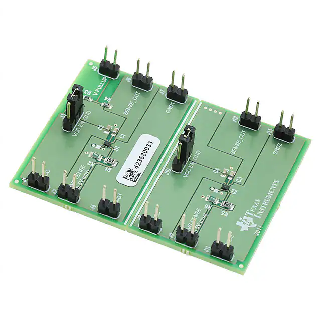
This section provides the TPS389XEVM board layout.
J3
J5
R4
R3
J1
J2
J6
R2
1
R1
C2
U1
C1
J4
J7
J8
J10
J12
J9
R6
1
J11
R5
C4
U2
C3
J13
Figure 4. Assembly Layer (Top)
SLVU524A – August 2011 – Revised September 2011
Submit Documentation Feedback
TPS389xA-xP-EVM047 Evaluation Modules
Copyright © 2011, Texas Instruments Incorporated
7
�Board Layout
www.ti.com
Figure 5. Top Layer Routing
8
TPS389xA-xP-EVM047 Evaluation Modules
SLVU524A – August 2011 – Revised September 2011
Submit Documentation Feedback
Copyright © 2011, Texas Instruments Incorporated
�Board Layout
www.ti.com
Figure 6. Bottom Layer Routing
SLVU524A – August 2011 – Revised September 2011
Submit Documentation Feedback
TPS389xA-xP-EVM047 Evaluation Modules
Copyright © 2011, Texas Instruments Incorporated
9
�Bill of Materials
6
www.ti.com
Bill of Materials
Table 4. EVM Assembly Associated with EVM Orderable
PWR047001
PWR047002
PWR047003
PWR047004
COUNT
COUNT
COUNT
COUNT
RefDes
Value
Description
Size
Part Number
2
2
2
2
C1 C3
0.047uF
Capacitor, Ceramic, X7R, 10V 10%
0603
STD
2
2
2
2
C2 C4
0.1uF
Capacitor, Ceramic, X7R, 50V 10%
0603
STD
11
11
11
11
J1-2 J4-9
J11-13
PEC02SAAN
Header, Male 2-pin, 100mil spacing
0.100 inch x 2
PEC02SAAN
2
2
2
2
J3 J10
PEC03SAAN
Header, Male 3-pin, 100mil spacing
0.100 inch x 3
PEC03SAAN
2
2
2
2
R1 R5
1.00M
Resistor, 1/8W, 0.1%, ±25ppm/°C
0805
ERA-6AEB105V
2
2
2
2
R2 R6
191k
Resistor, 1/8W, 0.1%, ±25ppm/°C
0805
TNPW0805191KBEEA
1
1
1
1
R3
0 ohm
Resistor, Chip, 1/16W, 1%
0402
STD
1
1
1
1
R4
49.9k
Resistor, Chip, 1/16W, 1%
0402
STD
1
0
0
0
U1
TPS3897ADRY
IC, Single Chan Adjustable Supervisory
DSBGA
TPS3897ADRY
0
0
1
0
U1
TPS3898ADRY
IC, Single Chan Adjustable Supervisory
DSBGA
TPS3898ADRY
0
0
0
1
U2
TPS3895ADRY
IC, Single Chan Adjustable Supervisory
DSBGA
TPS3895ADRY
0
1
0
0
U2
TPS3896ADRY
IC, Single Chan Adjustable Supervisory
DSBGA
TPS3896ADRY
0
1
0
0
U1
TPS3897PDRY
IC, Single Chan Adjustable Supervisory
DSBGA
TPS3897PDRY
0
0
0
1
U1
TPS3898PDRY
IC, Single Chan Adjustable Supervisory
DSBGA
TPS3898PDRY
0
0
1
0
U2
TPS3895PDRY
IC, Single Chan Adjustable Supervisory
DSBGA
TPS3895PDRY
1
0
0
0
U2
TPS3896PDRY
IC, Single Chan Adjustable Supervisory
DSBGA
TPS3896PDRY
2
2
2
2
--
Shunt
Shunt, Black
100-mil
929950-00
1
1
1
1
--
Board
PCB, 2.300 In x 1.730 In x 0.062 In
Notes:
1. These assemblies are ESD sensitive, ESD precautions shall be observed.
PWR047
SPACER
2. These assemblies must be clean and free from flux and all contaminants. Use of no clean flux is not acceptable.
3. These assemblies must comply with workmanship standards IPC-A-610 Class 2.
4. Ref designators marked with an asterisk ('**') cannot be substituted. All other components can be substituted with equivalent MFG's components.
5. Install label after final wash. Text shall be 8 pt font. Text shall be per Table 5.
6. Score the board per score line but do not separate them.
10
SLVU524A – August 2011 – Revised September 2011
Submit Documentation Feedback
TPS389xA-xP-EVM047 Evaluation Modules
Copyright © 2011, Texas Instruments Incorporated
�Bill of Materials
www.ti.com
Table 5.
Assembly Number
text
PWR047-001
TPS3897A-6P-EVM047
PWR047-002
TPS3897P-6A-EVM047
PWR047-003
TPS3898A-5P-EVM047
PWR047-004
TPS3898P-5A-EVM047
SLVU524A – August 2011 – Revised September 2011
Submit Documentation Feedback
TPS389xA-xP-EVM047 Evaluation Modules
Copyright © 2011, Texas Instruments Incorporated
11
�Evaluation Board/Kit Important Notice
Texas Instruments (TI) provides the enclosed product(s) under the following conditions:
This evaluation board/kit is intended for use for ENGINEERING DEVELOPMENT, DEMONSTRATION, OR EVALUATION
PURPOSES ONLY and is not considered by TI to be a finished end-product fit for general consumer use. Persons handling the
product(s) must have electronics training and observe good engineering practice standards. As such, the goods being provided are
not intended to be complete in terms of required design-, marketing-, and/or manufacturing-related protective considerations,
including product safety and environmental measures typically found in end products that incorporate such semiconductor
components or circuit boards. This evaluation board/kit does not fall within the scope of the European Union directives regarding
electromagnetic compatibility, restricted substances (RoHS), recycling (WEEE), FCC, CE or UL, and therefore may not meet the
technical requirements of these directives or other related directives.
Should this evaluation board/kit not meet the specifications indicated in the User’s Guide, the board/kit may be returned within 30
days from the date of delivery for a full refund. THE FOREGOING WARRANTY IS THE EXCLUSIVE WARRANTY MADE BY
SELLER TO BUYER AND IS IN LIEU OF ALL OTHER WARRANTIES, EXPRESSED, IMPLIED, OR STATUTORY, INCLUDING
ANY WARRANTY OF MERCHANTABILITY OR FITNESS FOR ANY PARTICULAR PURPOSE.
The user assumes all responsibility and liability for proper and safe handling of the goods. Further, the user indemnifies TI from all
claims arising from the handling or use of the goods. Due to the open construction of the product, it is the user’s responsibility to
take any and all appropriate precautions with regard to electrostatic discharge.
EXCEPT TO THE EXTENT OF THE INDEMNITY SET FORTH ABOVE, NEITHER PARTY SHALL BE LIABLE TO THE OTHER
FOR ANY INDIRECT, SPECIAL, INCIDENTAL, OR CONSEQUENTIAL DAMAGES.
TI currently deals with a variety of customers for products, and therefore our arrangement with the user is not exclusive.
TI assumes no liability for applications assistance, customer product design, software performance, or infringement of
patents or services described herein.
Please read the User’s Guide and, specifically, the Warnings and Restrictions notice in the User’s Guide prior to handling the
product. This notice contains important safety information about temperatures and voltages. For additional information on TI’s
environmental and/or safety programs, please contact the TI application engineer or visit www.ti.com/esh.
No license is granted under any patent right or other intellectual property right of TI covering or relating to any machine, process, or
combination in which such TI products or services might be or are used.
FCC Warning
This evaluation board/kit is intended for use for ENGINEERING DEVELOPMENT, DEMONSTRATION, OR EVALUATION
PURPOSES ONLY and is not considered by TI to be a finished end-product fit for general consumer use. It generates, uses, and
can radiate radio frequency energy and has not been tested for compliance with the limits of computing devices pursuant to part 15
of FCC rules, which are designed to provide reasonable protection against radio frequency interference. Operation of this
equipment in other environments may cause interference with radio communications, in which case the user at his own expense
will be required to take whatever measures may be required to correct this interference.
EVM Warnings and Restrictions
It is important to operate this EVM within the input voltage range of 0 V to 7 V and the output voltage range of 0 V to 7 V .
Exceeding the specified input range may cause unexpected operation and/or irreversible damage to the EVM. If there are
questions concerning the input range, please contact a TI field representative prior to connecting the input power.
Applying loads outside of the specified output range may result in unintended operation and/or possible permanent damage to the
EVM. Please consult the EVM User's Guide prior to connecting any load to the EVM output. If there is uncertainty as to the load
specification, please contact a TI field representative.
During normal operation, some circuit components may have case temperatures greater than 85° C. The EVM is designed to
operate properly with certain components above 85° C as long as the input and output ranges are maintained. These components
include but are not limited to linear regulators, switching transistors, pass transistors, and current sense resistors. These types of
devices can be identified using the EVM schematic located in the EVM User's Guide. When placing measurement probes near
these devices during operation, please be aware that these devices may be very warm to the touch.
Mailing Address: Texas Instruments, Post Office Box 655303, Dallas, Texas 75265
Copyright © 2011, Texas Instruments Incorporated
�IMPORTANT NOTICE
Texas Instruments Incorporated and its subsidiaries (TI) reserve the right to make corrections, modifications, enhancements, improvements,
and other changes to its products and services at any time and to discontinue any product or service without notice. Customers should
obtain the latest relevant information before placing orders and should verify that such information is current and complete. All products are
sold subject to TI’s terms and conditions of sale supplied at the time of order acknowledgment.
TI warrants performance of its hardware products to the specifications applicable at the time of sale in accordance with TI’s standard
warranty. Testing and other quality control techniques are used to the extent TI deems necessary to support this warranty. Except where
mandated by government requirements, testing of all parameters of each product is not necessarily performed.
TI assumes no liability for applications assistance or customer product design. Customers are responsible for their products and
applications using TI components. To minimize the risks associated with customer products and applications, customers should provide
adequate design and operating safeguards.
TI does not warrant or represent that any license, either express or implied, is granted under any TI patent right, copyright, mask work right,
or other TI intellectual property right relating to any combination, machine, or process in which TI products or services are used. Information
published by TI regarding third-party products or services does not constitute a license from TI to use such products or services or a
warranty or endorsement thereof. Use of such information may require a license from a third party under the patents or other intellectual
property of the third party, or a license from TI under the patents or other intellectual property of TI.
Reproduction of TI information in TI data books or data sheets is permissible only if reproduction is without alteration and is accompanied
by all associated warranties, conditions, limitations, and notices. Reproduction of this information with alteration is an unfair and deceptive
business practice. TI is not responsible or liable for such altered documentation. Information of third parties may be subject to additional
restrictions.
Resale of TI products or services with statements different from or beyond the parameters stated by TI for that product or service voids all
express and any implied warranties for the associated TI product or service and is an unfair and deceptive business practice. TI is not
responsible or liable for any such statements.
TI products are not authorized for use in safety-critical applications (such as life support) where a failure of the TI product would reasonably
be expected to cause severe personal injury or death, unless officers of the parties have executed an agreement specifically governing
such use. Buyers represent that they have all necessary expertise in the safety and regulatory ramifications of their applications, and
acknowledge and agree that they are solely responsible for all legal, regulatory and safety-related requirements concerning their products
and any use of TI products in such safety-critical applications, notwithstanding any applications-related information or support that may be
provided by TI. Further, Buyers must fully indemnify TI and its representatives against any damages arising out of the use of TI products in
such safety-critical applications.
TI products are neither designed nor intended for use in military/aerospace applications or environments unless the TI products are
specifically designated by TI as military-grade or "enhanced plastic." Only products designated by TI as military-grade meet military
specifications. Buyers acknowledge and agree that any such use of TI products which TI has not designated as military-grade is solely at
the Buyer's risk, and that they are solely responsible for compliance with all legal and regulatory requirements in connection with such use.
TI products are neither designed nor intended for use in automotive applications or environments unless the specific TI products are
designated by TI as compliant with ISO/TS 16949 requirements. Buyers acknowledge and agree that, if they use any non-designated
products in automotive applications, TI will not be responsible for any failure to meet such requirements.
Following are URLs where you can obtain information on other Texas Instruments products and application solutions:
Products
Applications
Audio
www.ti.com/audio
Communications and Telecom www.ti.com/communications
Amplifiers
amplifier.ti.com
Computers and Peripherals
www.ti.com/computers
Data Converters
dataconverter.ti.com
Consumer Electronics
www.ti.com/consumer-apps
DLP® Products
www.dlp.com
Energy and Lighting
www.ti.com/energy
DSP
dsp.ti.com
Industrial
www.ti.com/industrial
Clocks and Timers
www.ti.com/clocks
Medical
www.ti.com/medical
Interface
interface.ti.com
Security
www.ti.com/security
Logic
logic.ti.com
Space, Avionics and Defense
www.ti.com/space-avionics-defense
Power Mgmt
power.ti.com
Transportation and Automotive www.ti.com/automotive
Microcontrollers
microcontroller.ti.com
Video and Imaging
RFID
www.ti-rfid.com
OMAP Mobile Processors
www.ti.com/omap
Wireless Connctivity
www.ti.com/wirelessconnectivity
TI E2E Community Home Page
www.ti.com/video
e2e.ti.com
Mailing Address: Texas Instruments, Post Office Box 655303, Dallas, Texas 75265
Copyright © 2011, Texas Instruments Incorporated
�


 工商网监
湘ICP备2023018690号
工商网监
湘ICP备2023018690号
