www.ti.com
Table of Contents
User’s Guide
TPS40077 Buck Controller Evaluation Module User's
Guide
ABSTRACT
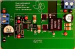
The TPS40077EVM-001 evaluation module (EVM) is a synchronous buck converter providing a fixed 1.8-V
output at up to 10 A from a 12-V input bus. The EVM is designed to start up from a single supply; no additional
bias voltage is required for start-up. The TPS40077 reduced-pin count synchronous buck controller used in
the EVM employs predictive gate drive. This feature provides improved efficiency by eliminating shoot-through
switching current,and minimizing the reverse-conduction time of the synchronous rectifier FET.
Table of Contents
1 Introduction.............................................................................................................................................................................2
1.1 Description......................................................................................................................................................................... 2
1.2 Applications........................................................................................................................................................................2
1.3 Features............................................................................................................................................................................. 2
2 TPS40077EVM-001 Electrical Performance Specifications................................................................................................ 3
3 Schematic................................................................................................................................................................................4
3.1 Adjusting Output Voltage (R3 and R13)............................................................................................................................. 5
3.2 Disable (J3)........................................................................................................................................................................ 5
3.3 Test Set Up.........................................................................................................................................................................5
3.4 Equipment Setup................................................................................................................................................................6
3.5 Start-Up/Shut Down Procedure..........................................................................................................................................7
3.6 Control Loop Gain and Phase Measurement Procedure................................................................................................... 8
3.7 Equipment Shutdown......................................................................................................................................................... 8
4 TPS40077EVM Typical Performance Data and Characteristic Curves...............................................................................9
4.1 Efficiency............................................................................................................................................................................9
4.2 Line and Load Regulation.................................................................................................................................................. 9
4.3 Output Ripple................................................................................................................................................................... 10
4.4 Transient Response......................................................................................................................................................... 10
4.5 Bode Plot..........................................................................................................................................................................11
5 EVM Assembly Drawings and Layout.................................................................................................................................12
6 List of Materials.....................................................................................................................................................................14
7 Revision History................................................................................................................................................................... 14
Trademarks
All trademarks are the property of their respective owners.
SLVU192B – FEBRUARY 2007 – REVISED JANUARY 2022
TPS40077 Buck Controller Evaluation Module User's Guide
Submit Document Feedback
Copyright © 2022 Texas Instruments Incorporated
1
�Introduction
www.ti.com
1 Introduction
1.1 Description
The TPS40077EVM-001 is designed to use a 12-V (8 V-to-16 V) bus to produce a high current, regulated 1.8-V
output at up to 10 A of load current. The TPS40077EVM-001 demonstrates the use of the TPS40077 in a typical
12-V bus to low-voltage application, while providing a number of test points to evaluate the performance of the
TPS40077. The EVM can be modified to support output voltages from 0.9 V to 3.3 V by changing a single
resistor.
1.2 Applications
•
•
•
•
Non-isolated, medium-current point-of-load and low-voltage bus converters
Networking equipment
Telecommunications equipment
DC-power distributed systems
1.3 Features
•
•
•
•
•
•
•
•
2
8-V to 16-V input range
1.8-V fixed output, adjustable with a single resistor
10-A DC steady-state output current
300-kHz switching frequency
Single main switch N-channel MOSFET and single synchronous rectifier N-channel MOSFET
Double-sided PCB with all components on top side
Active converter uses less than 2.4 square inches – 1.0 inches × 2.4 inches
Convenient test points for probing critical waveforms and non-invasive loop response testing
TPS40077 Buck Controller Evaluation Module User's Guide
SLVU192B – FEBRUARY 2007 – REVISED JANUARY 2022
Submit Document Feedback
Copyright © 2022 Texas Instruments Incorporated
�www.ti.com
TPS40077EVM-001 Electrical Performance Specifications
2 TPS40077EVM-001 Electrical Performance Specifications
Table 2-1. TPS40077EVM-001 Electrical and Performance Specifications
PARAMETER
NOTES AND CONDITIONS
MIN
NOM
MAX
8
12
16
UNITS
INPUT CHARACTERISTICS
VIN
Input voltage
V
IIN
Input current
VIN = nom, IOUT = max
1.7
1.8
A
No-load input current
VIN = nom, IOUT = 0A
80
100
mA
VIN_UVLO
Input UVLO
IOUT = min to max
5.4
6
6.6
V
VIN_ONV
Input ONV
IOUT = min to max
6.3
7
7.7
V
1.75
1.8
1.85
V
OUTPUT CHARACTERISTICS
VOUT
Output voltage
VIN = nom, IOUT = nom
Line regulation
VIN = min to max, IOUT = nom
0.5%
Load regulation
VIN = nom, IOUT = min to max
0.5%
Output ripple voltage
VOUT_ripple VIN = nom, IOUT = max
Output current
IOUT VIN = min to max
Output overcurrent inception point
IOCP VIN = nom, VOUT = VOUT – 5%
40
mVpp
0
5
10
A
12.25
19.4
34
A
Transient response
ΔI
Load step
IOUT_max to 0.2 × IOUT _max
Load slew rate
8
A
1
A/μsec
Overshoot
300
mV
Settling time
0.1
msec
SYSTEMS CHARACTERISTICS
fSW
Switching frequency
ηpk
Peak efficiency
VIN = nom, IOUT = min to max
240
η
Full-load efficiency
VIN = nom, IOUT = max
Top
Operating temperature range
VIN = min to max, IOUT = min to max
300
360
kHz
85
°C
90%
89%
–40
25
MECHANICAL CHARACTERISTICS
W
Dimensions (active area)
Width
L
Length
h
Component height
1
ins
2.4
ins
0.41
ins
NOTE 1: Voltage accuracy effected by resistor tolerance.
SLVU192B – FEBRUARY 2007 – REVISED JANUARY 2022
TPS40077 Buck Controller Evaluation Module User's Guide
Submit Document Feedback
Copyright © 2022 Texas Instruments Incorporated
3
�Schematic
www.ti.com
3 Schematic
+
+
For reference only. See Table 6-1 for specific values.
Figure 3-1. TPS40077EVM-001 Schematic
4
TPS40077 Buck Controller Evaluation Module User's Guide
SLVU192B – FEBRUARY 2007 – REVISED JANUARY 2022
Submit Document Feedback
Copyright © 2022 Texas Instruments Incorporated
�www.ti.com
Schematic
3.1 Adjusting Output Voltage (R3 and R13)
The regulated output voltage can be adjusted within a limited range by changing the ground resistors in the
feedback resistor-divider (R3, R13).
Table 3-1 contains common values for R3 and R13 to generate popular output voltages. The
TPS40077EVM-001 is stable through these output voltages but the efficiency can suffer as the power stage
is optimized for the 1.8-V output.
Table 3-1. Adjusting VOUT With R3
VOUT
R3
R13
1.2 V
9.53 kΩ
62.0 kΩ
1.5 V
5.36 kΩ
140 kΩ
1.8 V
4.42 kΩ
24.9 kΩ
2.5 V
2.37 kΩ
71.5 kΩ
3.3 V
1.60 kΩ
220 kΩ
3.2 Disable (J3)
The TPS40077EVM-001 provides a Disable input (J3) that allows the user to evaluate the Enable/Disable
function of the TPS40077. When a short is applied across the pins of J3, the TPS40077 controller is disabled
and the EVM shuts down. When the TPS40077 is disabled, both FET drivers are off.
3.3 Test Set Up
3.3.1 Equipment
3.3.1.1 Voltage Source
V12V_IN
The input voltage source (V12V_IN) should be a 0-V to 16-V variable DC source capable of 5 ADC. Connect
V12V_IN to J1 as shown in Figure 3-3.
3.3.1.2 Meters
•
•
•
A1: 0-5 ADC, ammeter
V1: V12V_IN, 0-V to 16-V voltmeter
V2: V1V5_OUT 0-V to 5-V voltmeter
3.3.1.3 Loads
LOAD1
The output load (LOAD1) must be a constant-current mode electronic load capable of 0-A to 15-A DC at 1.8 V.
3.3.1.4 Oscilloscope
A digital or analog oscilloscope can be used to measure the ripple voltage on VOUT. The oscilloscope should be
set to the following to measure output ripple:
•
•
•
•
•
1-MΩ impedance
20-MHz bandwidth
AC coupling
1-μs/division horizontal resolution
20-mV/division vertical resolution
TP9 and TP10 can be used to measure the output ripple voltage by placing the oscilloscope probe tip through
TP9 and holding the ground barrel to TP10 as shown in Figure 3-2. For a hands-free approach, the loop in TP10
can be cut and opened to cradle the probe barrel. Using a leaded ground connection must be avoided because it
induces additional noise due to its large ground-loop area.
SLVU192B – FEBRUARY 2007 – REVISED JANUARY 2022
TPS40077 Buck Controller Evaluation Module User's Guide
Submit Document Feedback
Copyright © 2022 Texas Instruments Incorporated
5
�Schematic
www.ti.com
Metal Ground Barrel
Probe Tip
TP9
TP10
Tip and Barrel Vout Ripple
Measurement
Figure 3-2. Output Ripple Measurement – Tip and Barrel Using TP9 and TP10
3.3.1.5 Recommended Wire Gauge
V12V_IN to J1
The connection between the source voltage, V12V_IN, and J1 can carry as much as 3 ADC. The minimum
recommended wire size is AWG #16 with the total length of wire less than four feet (2-feet input, 2-feet return).
J2 to LOAD1 (Power)
The power connection between J2 and LOAD1 can carry as much as 15 ADC. The minimum recommended wire
size is 2 × AWG #16, with the total length of wire less than four feet (2-feet output, 2-feet return).
3.4 Equipment Setup
Figure 3-3 shows the basic recommended test set up to evaluate the TPS40077EVM-001. Note that although
the return for J1 and J2 are the same, the connections should remain separate as shown in Figure 3-2.
3.4.1 Procedure
1. Working at an ESD workstation, make sure that any wrist straps, bootstraps, or mats are connected
referencing the user to earth ground before power is applied to the EVM. An electrostatic smock and safety
glasses should also be worn.
2. Prior to connecting the DC input source, V12V_IN, it is advisable to limit the source current from V12V_IN to
5.0-A maximum. Make sure V12V_IN is initially set to 0 V and connected as shown in Figure 3-3.
3. Connect an Ammeter A1 as shown in Figure 3-3.
4. Connect Voltmeter V1 to TP1 and TP2 as shown in Figure 3-3.
5. Connect LOAD1 to J2 as shown in Figure 3-3. Set LOAD1 to constant current mode to sink 0 A DC before
V12V_IN is applied.
6. Connect Voltmeter V2 to Output J2 as shown in Figure 3-3.
7. Connect an oscilloscope probe to TP9 and TP10 as shown in Figure 3-2.
6
TPS40077 Buck Controller Evaluation Module User's Guide
SLVU192B – FEBRUARY 2007 – REVISED JANUARY 2022
Submit Document Feedback
Copyright © 2022 Texas Instruments Incorporated
�www.ti.com
Schematic
3.4.2 Diagram
+ V2 -
LOAD1
Oscilloscope
1M!, AC
.
1.8V
0 to 10A
+
20MH
z
-
V12V_IN
0 to 15V
+ V1 -
See figure 2 for tip
and barrel
measurement
A1
-
+
Figure 3-3. TPS40077EVM-001 Recommended Test Setup
+ V2 -
LOAD1
1.8V
0 to 10A
+
-
V12V_IN
0 to 15V
+ V1 -
Network
Analyzer
A1
-
+
CHA CHB
See section 3.7
Figure 3-4. Control Loop Measurement Setup
3.5 Start-Up/Shut Down Procedure
1. Increase V12V_IN from 0 VDC to 12 VDC.
2. Vary LOAD1 from 0 ADC–10 ADC.
3. Vary V12V_IN from 8 VDC to 16 VDC.
SLVU192B – FEBRUARY 2007 – REVISED JANUARY 2022
TPS40077 Buck Controller Evaluation Module User's Guide
Submit Document Feedback
Copyright © 2022 Texas Instruments Incorporated
7
�Schematic
www.ti.com
4. Decrease LOAD1 to 0 A.
3.6 Control Loop Gain and Phase Measurement Procedure
1.
2.
3.
4.
5.
6.
Connect a 1-kHz to 1-MHz isolation transformer to TP3 and TP6 as shown in Figure 3-4.
Connect an .input-signal amplitude-measurement probe (channel A) to TP3 as shown in Figure 3-4
Connect an output-signal amplitude measurement probe (channel B) to TP6 as shown in Figure 3-4.
Connect the ground lead of channel A and channel B to TP8 as shown in Figure 3-4.
Inject 25-mV or less signal across TP3 and TP6 through an isolation transformer.
Sweep frequency from 1 kHz to 1 MHz with 10 Hz or lower post filter.
20 LOG ChannelB
ChannelA .
7. Control-loop gain can be measured by
8. Control-loop phase is measured by the phase difference between channel A and channel B.
9. Disconnect an isolation transformer from TP3 and TP6 before making other measurements (signal injection
into feedback can interfere with accuracy of other measurements).
ǒ
Ǔ
3.7 Equipment Shutdown
1. Shut down the oscilloscope.
2. Shut down LOAD1.
3. Shut down V12V_IN.
8
TPS40077 Buck Controller Evaluation Module User's Guide
SLVU192B – FEBRUARY 2007 – REVISED JANUARY 2022
Submit Document Feedback
Copyright © 2022 Texas Instruments Incorporated
�www.ti.com
TPS40077EVM Typical Performance Data and Characteristic Curves
4 TPS40077EVM Typical Performance Data and Characteristic Curves
Figure 4-1 through Figure 4-6 present typical performance curves for the TPS40077EVM-001. Since actual
performance data can be affected by measurement techniques and environmental variables, these curves are
presented for reference and may differ from actual field measurements.
4.1 Efficiency
100
VIN = 8.0 V
90
h - Efficiency - %
80
VIN = 16.0 V
70
VIN = 12.0 V
60
50
40
30
20
10
0
0
1
2
3
4
5
6
7
IO- Load Current - A
8
9
10
Figure 4-1. TPS40077EVM-001 Efficiency
4.2 Line and Load Regulation
1.850
VO - Output Voltage - V
1.830
1.810
VIN = 8.0 V
1.790
1.770
VIN = 12.0 V
VIN = 16.0 V
1.750
0
1
2
3
4
5
6
7
IO - Load Current - A
8
9
10
Figure 4-2. TPS40077EVM-001 Line and Load Regulation
SLVU192B – FEBRUARY 2007 – REVISED JANUARY 2022
TPS40077 Buck Controller Evaluation Module User's Guide
Submit Document Feedback
Copyright © 2022 Texas Instruments Incorporated
9
�TPS40077EVM Typical Performance Data and Characteristic Curves
www.ti.com
4.3 Output Ripple
VIN= 12 V, VOUT= 1.8 V, IOUT= 10 A
Figure 4-3. TPS40077EVM-001 Typical Output Ripple
4.4 Transient Response
Slew rate = 1 A/ms, VIN = 12 V, VOUT = 1.8 V
CH1 = VOUT
CH4 = IOUT
Figure 8. Load Transient, 2A to 10A, slew rate = 1A/! s, VIN = 12V, VOUT = 1.8V
Figure 4-4. Load Transient, 2 A to 10 A
10
TPS40077 Buck Controller Evaluation Module User's Guide
SLVU192B – FEBRUARY 2007 – REVISED JANUARY 2022
Submit Document Feedback
Copyright © 2022 Texas Instruments Incorporated
�www.ti.com
TPS40077EVM Typical Performance Data and Characteristic Curves
Slew rate = 1 A/ms, VIN = 12 V, VOUT = 1.8 V
CH1 = VOUT
CH4 = IOUT
Figure 9. Load Transient, 10A to 2A, slew rate = 1A/! s, VIN = 12V, VOUT = 1.8V
Figure 4-5. Load Transient, 10 A to 2 A
4.5 Bode Plot
48
180
36
135
24
90
12
45
Gain
0
0
–12
–24
–36
–48
0.1
Phase - °
Gain - dB
Phase
–45
VIN= 12 V
VOUT= 1.8 V
IOUT= 10 A
Crossover frequency = 30.7 kHz
Phase margin = 52.5°
1
10
Frequency - kHz
–90
–135
–180
100
1000
Figure 4-6. Typical Bode Plot
SLVU192B – FEBRUARY 2007 – REVISED JANUARY 2022
TPS40077 Buck Controller Evaluation Module User's Guide
Submit Document Feedback
Copyright © 2022 Texas Instruments Incorporated
11
�EVM Assembly Drawings and Layout
www.ti.com
5 EVM Assembly Drawings and Layout
Figure 5-1 through Figure 5-3 show the design of the TPS40077EVM-001 printed circuit board. The EVM has
been designed using a double-sided, 2-oz copper-clad circuit board, with all components on the top side to allow
the user to easily view, probe, and evaluate the TPS40077 in a practical application. Moving components to
both sides of the PCB or using additional internal layers can offer additional size reduction for space-constrained
systems.
Figure 5-1. TPS40077EVM-001 Component Placement (Viewed from Top)
Figure 5-2. TPS40077EVM-001 Top Copper (Viewed from Top)
12
TPS40077 Buck Controller Evaluation Module User's Guide
SLVU192B – FEBRUARY 2007 – REVISED JANUARY 2022
Submit Document Feedback
Copyright © 2022 Texas Instruments Incorporated
�www.ti.com
EVM Assembly Drawings and Layout
Figure 5-3. TPS40077EVM-001 Bottom Copper (X-Ray View from Top)
SLVU192B – FEBRUARY 2007 – REVISED JANUARY 2022
TPS40077 Buck Controller Evaluation Module User's Guide
Submit Document Feedback
Copyright © 2022 Texas Instruments Incorporated
13
�List of Materials
www.ti.com
6 List of Materials
Table 6-1 lists the EVM components as configured according to the schematic shown in Figure 3-1.
Table 6-1. Bill of Materials
COUNT
RefDes
Value
Description
Size
Part Number
MFR
1
C1
470 μF
Capacitor, Aluminum, 470 μF, 25 V, 20%
0.457 x 0.406
EEVFK1E471P
Panasonic
3
C12, C14, C15
22 μF
Capacitor, Ceramic, 22 μF, 16 V, X5R, 20%
1812
C4532X5R1C226MT
TDK
2
C6, C13
2.2 nF
Capacitor, Ceramic, 25 V, X7R 20%
0603
Std
Vishay
1
C16
470 μF
Capacitor, Aluminum, SM, 6.3 V, 300 mΩ (FK
series)
8x10mm
FK-Series
Panasonic
1
C17
47 μF
Capacitor, Ceramic, 47 μF, 6.3 V, X5R, 20%
1812
C4532X5R0J476MT
TDK
2
C2, C10
0.1 μF
Capacitor, Ceramic, 25 V, X7R, 20%
0603
Std
Vishay
1
C3
15 nF
Capacitor, Ceramic, 25 V, X7R, 20%
0603
Std
Vishay
1
C4
680 pF
Capacitor, Ceramic, 25 V, X7R, 20%
0603
Std
Vishay
1
C5
3900 pF
Capacitor, Ceramic, 25 V, X7R 20%
0603
Std
Vishay
1
C7
10 pF
Capacitor, Ceramic, 25 V, COG 20%
0603
Std
Vishay
2
C8, C11
0.1 μF
Capacitor, Ceramic, 25 V, X7R, 20%
0603
Std
Vishay
1
C9, C18
1 μF
Capacitor, Ceramic, 25 V, X7R, 20%
0805
Std
Vishay
1
D1
Diode, Schottky, 200 mA, 30 V
SOT23
BAT54
Vishay
1
L1
Inductor, SMT, 2.5 μH, 16.5 A, 3.4 mΩ
0.515 × 0.516
MLC1550-252ML
Coiltronics
1
Q1
MOSFET, NChannel, 30 V, 18 A, 8.0 mΩ
PWRPAK S0-8
Si7860DP
Vishay
1
Q2
MOSFET, NChannel, 30 V, 18 A, 40 mΩ
PWRPAK S0-8
Si7886ADP
Vishay
1
R1
10 kΩ
Resistor, Chip, 1/16W, 1%
0603
Std
Std
1
R10
330 kΩ
Resistor, Chip, 1/16W, 1%
0603
Std
Std
1
R12
51 Ω
Resistor, Chip, 1/16W, 1%
0603
Std
Std
1
R13
24.9 kΩ
Resistor, Chip, 1/16W, 1%
0603
Std
Std
2
R2, R6
165 kΩ
Resistor, Chip, 1/16W, 1%
0603
Std
Std
1
R3
4.42 kΩ
Resistor, Chip, 1/16W, 1%
0603
Std
Std
2
R4, R11
0Ω
Resistor, Chip, 1/16W, 1%
0603
Std
Std
1
R5
3.48 kΩ
Resistor, Chip, 1/16W, 1%
0603
Std
Std
1
R7
5.90 kΩ
Resistor, Chip, 1/16W, 1%
0603
Std
Std
1
R8
953 Ω
Resistor, Chip, 1/16W, 1%
0603
Std
Std
1
R9
1.80 kΩ
Resistor, Chip, 1/16W, 1%
0603
Std
Std
1
U1
IC
PWP16
TPS40077PWP
Texas
Instruments
2.5 μH
7 Revision History
NOTE: Page numbers for previous revisions may differ from page numbers in the current version.
Changes from Revision A (March 2006) to Revision B (January 2022)
Page
• Updated the numbering format for tables, figures, and cross-references throughout the document. ................2
• Updated the user's guide title............................................................................................................................. 2
14
TPS40077 Buck Controller Evaluation Module User's Guide
SLVU192B – FEBRUARY 2007 – REVISED JANUARY 2022
Submit Document Feedback
Copyright © 2022 Texas Instruments Incorporated
�IMPORTANT NOTICE AND DISCLAIMER
TI PROVIDES TECHNICAL AND RELIABILITY DATA (INCLUDING DATA SHEETS), DESIGN RESOURCES (INCLUDING REFERENCE
DESIGNS), APPLICATION OR OTHER DESIGN ADVICE, WEB TOOLS, SAFETY INFORMATION, AND OTHER RESOURCES “AS IS”
AND WITH ALL FAULTS, AND DISCLAIMS ALL WARRANTIES, EXPRESS AND IMPLIED, INCLUDING WITHOUT LIMITATION ANY
IMPLIED WARRANTIES OF MERCHANTABILITY, FITNESS FOR A PARTICULAR PURPOSE OR NON-INFRINGEMENT OF THIRD
PARTY INTELLECTUAL PROPERTY RIGHTS.
These resources are intended for skilled developers designing with TI products. You are solely responsible for (1) selecting the appropriate
TI products for your application, (2) designing, validating and testing your application, and (3) ensuring your application meets applicable
standards, and any other safety, security, regulatory or other requirements.
These resources are subject to change without notice. TI grants you permission to use these resources only for development of an
application that uses the TI products described in the resource. Other reproduction and display of these resources is prohibited. No license
is granted to any other TI intellectual property right or to any third party intellectual property right. TI disclaims responsibility for, and you
will fully indemnify TI and its representatives against, any claims, damages, costs, losses, and liabilities arising out of your use of these
resources.
TI’s products are provided subject to TI’s Terms of Sale or other applicable terms available either on ti.com or provided in conjunction with
such TI products. TI’s provision of these resources does not expand or otherwise alter TI’s applicable warranties or warranty disclaimers for
TI products.
TI objects to and rejects any additional or different terms you may have proposed. IMPORTANT NOTICE
Mailing Address: Texas Instruments, Post Office Box 655303, Dallas, Texas 75265
Copyright © 2022, Texas Instruments Incorporated
�