Product
Folder
Order
Now
Support &
Community
Tools &
Software
Technical
Documents
Reference
Design
TPS40192, TPS40193
SLUS719H – MARCH 2007 – REVISED MAY 2019
TPS4019x 4.5-V to 18-V Input, Voltage-Mode, Synchronous Buck Controller
With Power Good
1 Features
3 Description
•
•
•
•
•
TPS40192 and TPS40193 are cost-optimized
synchronous buck controllers that operate from 4.5 V
to 18 V input. These controllers implement a voltagemode control architecture with the switching
frequency fixed at either 600 kHz (TPS40192) or 300
kHz (TPS40193). The higher switching frequency
facilitates the use of smaller inductor and output
capacitors, thereby providing a compact powersupply solution. An adaptive anti-cross conduction
scheme is used to prevent shoot through current in
the power FETs.
1
•
•
•
•
•
•
•
Input Operating Voltage Range: 4.5 V to 18 V
Up to 20-A Output Currents
Supports Pre-Biased Outputs
0.5%, 591-mV Reference
Switching Frequency
– TPS40192: 600 kHz
– TPS40193: 300 kHz
Three Selectable Thermally Compensated ShortCircuit Protection Levels
Hiccup Restart from Faults
Internal 5-V Regulator
High-Side and Low-Side MOSFET ON-resistance
(RDS(on)) Current Sensing
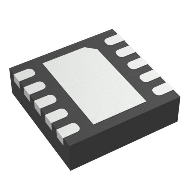
10-Pin 3 mm × 3 mm SON Package
Internal 4-ms Soft-Start Time
Thermal Shutdown Protection at 145°C
Short circuit detection is done by sensing the voltage
drop across the low-side MOSFET when it is on and
comparing it with a user selected threshold of 100
mV, 200 mV or 280 mV. The threshold is set with a
single external resistor connected from COMP to
GND. This resistor is sensed at startup and the
selected threshold is latched. Pulse-by-pulse limiting
(to prevent current runaway) is provided by sensing
the voltage across the high-side MOSFET when it is
on and terminating the cycle when the voltage drop
rises above a fixed threshold of 550 mV. When the
controller senses an output short circuit, both
MOSFETs are turned off and a timeout period is
observed before attempting to restart. This behavior
provides limited power dissipation in the event of a
sustained fault.
2 Applications
•
•
•
•
Cable Modem CPE
Digital Set Top Box
Graphics/Audio Cards
Entry Level and Mid-Range Servers
Device Information(1)
PART NUMBER
TPS40192
PACKAGE
VSON (10)
BODY SIZE (NOM)
3.00 mm × 3.00 mm
(1) For all available packages, see the orderable addendum at
the end of the data sheet.
Simplified Application Diagram
VIN
VOUT
ON/
OFF
TPS40192
TPS401923
External logic
supply 5-V or
less or BP5
+3.3V
PGD
1
ENABLE
2
FB
3
HDRV 10
SW
9
COMP
BOOT
8
4
VDD
LDRV
7
5
PGD
BP5
6
GND
VOUT
11
Copyright © 2016, Texas Instruments Incorporated
1
An IMPORTANT NOTICE at the end of this data sheet addresses availability, warranty, changes, use in safety-critical applications,
intellectual property matters and other important disclaimers. PRODUCTION DATA.
�TPS40192, TPS40193
SLUS719H – MARCH 2007 – REVISED MAY 2019
www.ti.com
Table of Contents
1
2
3
4
5
6
7
Features ..................................................................
Applications ...........................................................
Description .............................................................
Revision History.....................................................
Pin Configuration and Functions .........................
Specifications.........................................................
1
1
1
2
3
4
6.1
6.2
6.3
6.4
6.5
6.6
6.7
4
4
4
4
5
6
7
Absolute Maximum Ratings ......................................
ESD Ratings..............................................................
Recommended Operating Conditions.......................
Thermal Information ..................................................
Electrical Characteristics...........................................
Dissipation Ratings ...................................................
Typical Characteristics ..............................................
Detailed Description .............................................. 9
7.1
7.2
7.3
7.4
Overview ................................................................... 9
Functional Block Diagram ......................................... 9
Feature Description................................................... 9
Device Functional Modes........................................ 14
8
Application and Implementation ........................ 15
8.1 Application Information............................................ 15
8.2 Typical Application ................................................. 15
9 Power Supply Recommendations...................... 23
10 Layout................................................................... 24
10.1 Layout Guidelines ................................................. 24
10.2 Layout Examples................................................... 24
11 Device and Documentation Support ................. 26
11.1
11.2
11.3
11.4
11.5
11.6
11.7
11.8
Device Support......................................................
Documentation Support ........................................
Related Links ........................................................
Receiving Notification of Documentation Updates
Community Resources..........................................
Trademarks ...........................................................
Electrostatic Discharge Caution ............................
Glossary ................................................................
26
27
27
27
27
27
27
27
12 Mechanical, Packaging, and Orderable
Information ........................................................... 28
4 Revision History
NOTE: Page numbers for previous revisions may differ from page numbers in the current version.
Changes from Revision G (January 2019) to Revision H
•
Page
Editorial changes only, no technical revisions........................................................................................................................ 1
Changes from Revision F (November 2016) to Revision G
Page
•
Deleted last sentence in Enable Functionality ..................................................................................................................... 10
•
Deleted TPS40190 from Table 6 ......................................................................................................................................... 26
Changes from Revision E (May 2013) to Revision F
•
Page
Added Pin Configuration and Functions section, ESD Rating table, Feature Description section, Device Functional
Modes, Application and Implementation section, Power Supply Recommendations section, Layout section, Device
and Documentation Support section, and Mechanical, Packaging, and Orderable Information section .............................. 1
Changes from Revision D (July 2012) to Revision E
Page
•
Added clarity to Figure 15..................................................................................................................................................... 15
•
Added note regarding high-resistance resistor..................................................................................................................... 19
Changes from Revision C (August 2010) to Revision D
•
Page
Added text to the last paragraph in the Enable Functionality section. ................................................................................. 10
Changes from Revision B (September 2007) to Revision C
Page
•
Changed corrected label for pin 8 .......................................................................................................................................... 3
•
Changed corrected waveform .............................................................................................................................................. 11
2
Submit Documentation Feedback
Copyright © 2007–2019, Texas Instruments Incorporated
Product Folder Links: TPS40192 TPS40193
�TPS40192, TPS40193
www.ti.com
SLUS719H – MARCH 2007 – REVISED MAY 2019
5 Pin Configuration and Functions
DRC Package
10-Pin VSON
Top View
ENABLE 1
10 HDRV
FB 2
9 SW
COMP 3
VDD 4
Thermal
Pad
PGD 5
8
BOOT
7
LDRV
6
BP5
Pin Functions
PIN
NAME
NO.
BOOT
8
I/O
DESCRIPTION
I
Gate drive voltage for the high-side N-channel MOSFET. A 100-nF typical capacitor must be connected
between this pin and SW.
BP5
6
O
Output bypass for the internal regulator. Connect a capacitor with a value of at least 1-μF from this pin to GND.
Larger capacitors (up to 4.7 μF) can improve noise performance when using a low-side MOSFET with a gate
charge of 25 nC or greater. Low power, low noise loads may be connected here if desired. The sum of the
external load and the gate drive requirements must not exceed 50 mA. This regulator is turned off when
ENABLE is pulled low.
COMP
3
O
Output of the error amplifier.
ENABLE
1
I
Logic level input which starts or stops the controller from an external user command. A high-level turns the
controller on. A weak internal pullup holds this pin high so that the pin may be left floating if this function is not
used.
FB
2
I
Inverting input to the error amplifier. In normal operation the voltage on this pin is equal to the internal
reference voltage (591 mV typical)
HDRV
10
O
Bootstrapped output for driving the gate of the high-side N-channel FET.
LDRV
7
O
Output to the rectifier MOSFET gate
PGD
5
O
Open drain power good output
SW
9
I
Sense line for the adaptive anti-cross conduction circuitry. Serves as common connection for the flying highside MOSFET driver
VDD
4
I
Power input to the controller
G
Common reference for the device. Connect to the system GND.
Thermal pad
Copyright © 2007–2019, Texas Instruments Incorporated
Product Folder Links: TPS40192 TPS40193
Submit Documentation Feedback
3
�TPS40192, TPS40193
SLUS719H – MARCH 2007 – REVISED MAY 2019
www.ti.com
6 Specifications
6.1 Absolute Maximum Ratings
over operating free-air temperature range unless otherwise noted (1)
VDD, ENABLE
SW
Input voltage
MIN
MAX
–0.3
20
–5
25
BOOT, HDRV
–0.3
30
BOOT-SW, HDRV-SW (differential from BOOT or HDRV to SW)
–0.3
6
COMP, FB, BP5, LDRV, PGD
–0.3
6
Operating junction temperature, TJ
–40
150
Storage temperature, Tstg
–55
150
(1)
UNIT
V
°C
Stresses beyond those listed under "absolute maximum ratings" may cause permanent damage to the device. These are stress ratings
only, and functional operation of the device at these or any other conditions beyond those indicated under "recommended operating
conditions" is not implied. Exposure to absolute-maximum-rated conditions for extended periods may affect device reliability.
6.2 ESD Ratings
VALUE
Electrostatic
discharge
V(ESD)
(1)
(2)
Human-body model (HBM), per ANSI/ESDA/JEDEC JS-001 (1)
±2500
Charged-device model (CDM), per JEDEC specification JESD22C101 (2)
±1500
UNIT
V
JEDEC document JEP155 states that 500-V HBM allows safe manufacturing with a standard ESD control process.
JEDEC document JEP157 states that 250-V CDM allows safe manufacturing with a standard ESD control process.
6.3 Recommended Operating Conditions
MIN
MAX
UNIT
VVDD
Input voltage
4.5
18
V
TJ
Operating Junction temperature
-40
125
°C
6.4 Thermal Information
TPS40192
THERMAL METRIC (1)
DRC (VSON)
UNIT
10 PINS
RθJA
Junction-to-ambient thermal resistance
46.4
°C/W
RθJC(top)
Junction-to-case (top) thermal resistance
51.4
°C/W
RθJB
Junction-to-board thermal resistance
21.8
°C/W
ψJT
Junction-to-top characterization parameter
0.9
°C/W
ψJB
Junction-to-board characterization parameter
22.0
°C/W
RθJC(bot)
Junction-to-case (bottom) thermal resistance
6.6
°C/W
(1)
4
For more information about traditional and new thermal metrics, see the Semiconductor and IC Package Thermal Metrics application
report, SPRA953.
Submit Documentation Feedback
Copyright © 2007–2019, Texas Instruments Incorporated
Product Folder Links: TPS40192 TPS40193
�TPS40192, TPS40193
www.ti.com
SLUS719H – MARCH 2007 – REVISED MAY 2019
6.5 Electrical Characteristics
TJ = –40°C to 85°C, VVDD= 12 Vdc, all parameters at zero power dissipation (unless otherwise noted)
PARAMETER
TEST CONDITIONS
MIN
TYP
MAX
0°C ≤ TJ ≤ 85°C
588
591
594
-40°C ≤ TJ ≤ 85°C
585
591
594
UNIT
REFERENCE
VFB
Feedback voltage range
mV
INPUT SUPPLY
VVDD
IVDD
Input voltage range
4.5
Operating current
18
V
VENABLE = 3 V
2.5
4
mA
VENABLE = 0.6 V
45
70
μA
5.3
5.5
V
350
550
mV
ON-BOARD REGULATOR
Output voltage
VVDD > 6 V, I5VBP ≤ 10 mA
VDO
Regulator dropout voltage
VVDD - VBP5 , VVDD = 5 V, IBP5 ≤
25 mA
ISC
Regulator current limit threshold
IBP5
Average current
V5VBP
5.1
50
50
mA
OSCILLATOR
fSW
Switching frequency
VRMP
Ramp amplitude (1)
TPS40193
240
300
360
TPS40192
500
600
700
1
kHz
V
PWM
DMAX
Maximum duty cycle (1)
tON(min)
Minimum controlled pulse (1)
tDEAD
85%
110
Output driver dead time
HDRV off to LDRV on
50
LDRV off to HDRV on
25
ns
SOFT START
tSS
Soft-start time
3
4
tSSDLY
Soft-start delay time
2
tREG
Time to regulation
6
6
ms
ERROR AMPLIFIER
GBWP
Gain bandwidth product (1)
AOL
DC gain (1)
IIB
Input bias current (current out of FB pin)
IEAOP
Output source current
VFB = 0 V
1
IEAOM
Output sink current
VFB = 2 V
1
7
10
MHz
60
dB
100
nA
mA
SHORT CIRCUIT PROTECTION
tPSS(min)
Minimum pulse during short circuit (1)
250
(1)
tBLNK
Blanking time
60
tOFF
Off-time between restart attempts
VILIMH
(1)
Short circuit comparator threshold
voltage
Short circuit threshold voltage on highside MOSFET
120
30
50
160
200
240
RCOMP(GND) = 4 kΩ, TJ = 25°C
80
100
120
RCOMP(GND) = 12 kΩ, TJ = 25°C
228
280
342
TJ = 25°C
400
550
650
RCOMP(GND) = OPEN, TJ = 25°C
VILIM
90
ns
ms
mV
Specified by design. Not production tested.
Copyright © 2007–2019, Texas Instruments Incorporated
Product Folder Links: TPS40192 TPS40193
Submit Documentation Feedback
5
�TPS40192, TPS40193
SLUS719H – MARCH 2007 – REVISED MAY 2019
www.ti.com
Electrical Characteristics (continued)
TJ = –40°C to 85°C, VVDD= 12 Vdc, all parameters at zero power dissipation (unless otherwise noted)
PARAMETER
TEST CONDITIONS
MIN
TYP
MAX
3
6
3
UNIT
OUTPUT DRIVERS
RHDHI
High-side driver pullup resistance
VBOOT - VSW = 4.5 V, IHDRV = -100
mA
RHDLO
High-side driver pull-down resistance
VBOOT - VSW = 4.5 V, IHDRV = 100
mA
1.5
RLDHI
Low-side driver pullup resistance
ILDRV = -100 mA
2.5
5
RLDLO
Low-side driver pull-down resistance
ILDRV = 100 mA
0.8
1.5
tHRISE
High-side driver rise time (1)
15
35
tHFALL
High-side driver fall time (1)
10
25
tLRISE
Low-side driver rise time (1)
15
35
tLFALL
Low-side driver fall time (1)
10
25
CLOAD = 1 nF
Ω
ns
UVLO
VUVLO
Turn-on voltage
3.9
4.2
4.4
V
UVLOHYST
Hysteresis
700
800
900
mV
1.9
3
SHUTDOWN
VIH
High-level input voltage, ENABLE
VIL
Low-level input votlage, ENABLE
0.6
V
POWER GOOD
VOV
Feedback voltage limit for power good
650
VUV
Feedback voltage limit for power good
525
VPG_HYST
Powergood hysteresis voltage at FB pin
RPGD
Pulldown resistance of PGD pin
VFB = 0 V
7
50
Ω
IPDGLK
Leakage current
VFB = 0 V
7
12
μA
Bootstrap diode forward voltage
IBOOT = 5 mA
0.8
1.2
V
mV
30
BOOT DIODE
VDFWD
0.5
THERMAL SHUTDOWN
Junction shutdown temperature (1)
TJSD
TJSDH
Hysteresis
145
(1)
°C
20
6.6 Dissipation Ratings
PACKAGE
DRC
(1)
6
AIRFLOW (LFM)
RθJA High-K Board (1)
(°C/W)
Power Rating (W)
TA = 25°C
Power Rating (W)
TA = 85°C
0 (Natural Convection)
47.9
2.08
0.835
200
40.5
2.46
0.987
400
38.2
2.61
1.04
Ratings based on JEDEC High Thermal Conductivity (High K) Board. For more information on the test method, see TI Technical Brief
SZZA017.
Submit Documentation Feedback
Copyright © 2007–2019, Texas Instruments Incorporated
Product Folder Links: TPS40192 TPS40193
�TPS40192, TPS40193
www.ti.com
SLUS719H – MARCH 2007 – REVISED MAY 2019
6.7 Typical Characteristics
0.5
Rel Oscillator Frequency Change (%)
Rel Reference Voltage Change (%)
0.50
0.00
±0.05
±0.10
±0.15
±0.20
±0.25
±0.30
±0.35
±0.40
±0.45
±0.50
±40 ±25 ±10
5
20
35
50
65
80
95
0.0
±0.5
±1.0
±1.5
±2.0
±2.5
±3.0
±3.5
±4.0
±4.5
±40 ±25 ±10
110 125
5
Junction Temperature (°C)
35
50
65
80
95
110 125
Junction Temperature (°C)
Figure 1. Relative Reference Feedback Voltage vs Junction
Temperature
Figure 2. Relative Oscillator Frequency Change vs Junction
Temperature
2.5
Enable Threshold Voltage (V)
60
50
Shutdown Current (µA)
20
40
30
20
10
0
±40 ±25 ±10
5
20
35
50
65
80
95
2.0
1.5
1.0
0.5
Turn-on
Turn-off
0
±40 ±25 ±10
110 125
5
Junction Temperature (°C)
20 35 50 65 80
Junction Temperature (°C)
95
110 125
Figure 4. Enable Threshold Voltage vs Junction
Temperature
VENABLE < 0.6 V
Figure 3. Shutdown Input Current vs Junction Temperature
4.05
Current Limit Threshold (mV)
400
Soft-Start Time (ms)
4.00
3.95
3.90
3.85
3.80
3.75
±40 ±25 ±10
5
20 35 50 65 80
Junction Temperature (°C)
95
110 125
Figure 5. Soft-start Time vs Junction Temperature
350
300
RCOMP (NŸ)
12
4
Open
250
200
150
100
50
0
±40 ±25 ±10
5
20 35 50 65 80
Junction Temperature (°C)
95
110 125
Figure 6. Low-Side MOSFET Current Limit Threshold vs
Junction Temperature
Copyright © 2007–2019, Texas Instruments Incorporated
Product Folder Links: TPS40192 TPS40193
Submit Documentation Feedback
7
�TPS40192, TPS40193
SLUS719H – MARCH 2007 – REVISED MAY 2019
www.ti.com
800
6.3
700
6.1
5.9
600
Regulation Time (ms)
High-Side MOSFET Current Limit
Threshold (mV)
Typical Characteristics (continued)
500
400
300
200
5.5
5.3
5.1
4.7
5
20 35 50 65 80
Junction Temperature (°C)
95
4.4
±40 ±25 ±10
110 125
680
100
660
90
20 35 50 65 80
Junction Temperature (°C)
95
110 125
80
620
600
Overvoltage
Undervoltage
580
560
Supply Current (µA)
640
70
60
50
40
30
540
20
520
10
500
±40 ±25 ±10
5
Figure 8. Total Time to Regulation vs Junction Temperature
Figure 7. High-Side MOSFET Current Limit Threshold vs
Junction Temperature
Powergood Threshold Voltage (mV)
5.5
4.9
100
0
±40 ±25 ±10
5.7
0
5
20 35 50 65 80
Junction Temperature (°C)
95
110 125
Figure 9. Power-Good Threshold voltage vs Junction
Temperature
4
6
8
10
12
Input Voltage (V)
14
16
18
Figure 10. Shutdown Current vs Input Voltage
5
Relative Overcurrent Trip Point (A)
4.5
4
3.5
3
2.5
2
1.5
1
0.5
0
0.4
0.6
0.8
1.0
1.2
Freewheel Time (µs)
1.4
1.6
Figure 11. Relative Overcurrent Trip Point vs Freewheel Time
8
Submit Documentation Feedback
Copyright © 2007–2019, Texas Instruments Incorporated
Product Folder Links: TPS40192 TPS40193
�TPS40192, TPS40193
www.ti.com
SLUS719H – MARCH 2007 – REVISED MAY 2019
7 Detailed Description
7.1 Overview
The TPS40192 and TPS40193 devices are cost-optimized controllers providing all the necessary features to
construct a high performance DC/DC converter while keeping costs to a minimum. Support for pre-biased
outputs eliminates concerns about damaging sensitive loads during start-up. Strong gate drivers for the high-side
and rectifier N-channel MOSFETs decrease switching losses for increased efficiency. Adaptive gate drive timing
prevents shoot through and minimizes body diode conduction in the rectifier MOSFET, also increasing efficiency.
Selectable short circuit protection thresholds and hiccup recovery from a short circuit increase design flexibility
and minimize power dissipation in the event of a prolonged output fault. The dedicated ENABLE pin allows the
converter to be placed in a very low quiescent current shutdown mode. Internally fixed switching frequency and
soft-start time reduce external component count, simplifying design and layout, as well as reducing footprint and
cost. The 3-mm × 3- mm package size also contributes to a reduced overall converter footprint.
7.2 Functional Block Diagram
VDD
SC
+
OCL
FAULT
Fault
Controller
CLK
ENABLE
1
SD
+
OCH
SD
UVLO
Soft Start
Ramp
Generator
(VVDD ± 0.5 V)
VDD
5V
Regulator
4
BP5
6
COMP
3
4.2 V
+
5V
UVLO
SD
5V
CLK
Oscillator
FAULT
UVLO
591 mV
FB
SS
2
+
+
BOOT
10 HDRV
PWM Logic
and
Anti-Cross
Conduction
5V
UVLO FAULT
+
Error
Amplifier
8
9
SW
7
LDRV
5
PGD
SC Threshold Latch
FB
Thermal Pad
Short Circuit
Threshold
Selector
SD
SS
Powergood
Control
750 k:
SC: ±110 mV, ±200 mV, or ±280 mV
Copyright © 2016, Texas Instruments Incorporated
7.3 Feature Description
7.3.1 Voltage Reference
The band gap cell is designed with a trimmed 591-mV output. The 0.5% tolerance on the reference voltage
allows the user to design a very accurate power-supply.
7.3.2 Oscillator
The TPS40192 has a fixed internal switching frequency of 600 kHz. Tthe TPS40193 operates at a switching
frequency of 300 kHz.
Copyright © 2007–2019, Texas Instruments Incorporated
Product Folder Links: TPS40192 TPS40193
Submit Documentation Feedback
9
�TPS40192, TPS40193
SLUS719H – MARCH 2007 – REVISED MAY 2019
www.ti.com
Feature Description (continued)
7.3.3 UVLO
When the input voltage is below the UVLO threshold, the device holds all gate drive outputs in the low (OFF)
state. When the input rises above the UVLO threshold, and the ENABLE pin is above the turn ON threshold, the
oscillator begins to operate and the start-up sequence is allowed to begin. The UVLO level is internally fixed at
4.2 V.
7.3.4 Enable Functionality
A dedicated ENABLE pin simplifies a user-level interface design where no multiplexed functions exist. Another
benefit is a true low power shutdown mode of operation. When the ENABLE pin is pulled to GND, all
unnecessary functions, including the BP5 regulator, are turned off, reducing the device supply (IDD) current to 45µA. A functionally equivalent circuit of the enable circuitry shown in Figure 12.
VDD
4
7 0Ÿ
200 NŸ
1 NŸ
200 Ÿ
ENABLE
1
To
Enable
Chip
1 NŸ
300 NŸ
GND
5
Figure 12. Enable Pin Internal Circuitry
If the ENABLE pin is left floating, the chip starts automatically. The pin must be pulled to less than 600 mV to
ensure that the TPS40192 and TPS40193 devices is in shutdown mode. Note that the ENABLE pin is relatively
high impedance. Some applications generate enough nearby noise to cause the ENABLE pin to swing below the
600 mV threshold and give an erroneous shutdown commands to the rest of the device. There are two solutions
to solve this problem.
1. Place a capacitor from ENABLE to GND. A side effect of this is to delay the start of the converter while the
capacitor charges past the enable threshold
2. Place a resistor from VDD to ENABLE. This causes more current to flow in the shutdown mode, but does not
delay converter start-up. If a resistor is used, the total current into the ENABLE pin should be limited to no
more than 500 μA.
The ENABLE pin is self-clamping. The clamp voltage can be as low as 1 V with a 1-kΩ ground impedance. Due
to this self-clamping feature, the pullup impedance on the ENABLE pin should be selected to limit the sink
current to less than 500 µA. Driving the ENABLE pin with a low-impedance source voltage can result in damage
to the device. Because of the self-clamping feature, it requires care when connecting multiple ENABLE pins
together.
10
Submit Documentation Feedback
Copyright © 2007–2019, Texas Instruments Incorporated
Product Folder Links: TPS40192 TPS40193
�TPS40192, TPS40193
www.ti.com
SLUS719H – MARCH 2007 – REVISED MAY 2019
Feature Description (continued)
7.3.5 Start-Up Sequence and Timing
After input power is applied, the 5-V onboard regulator comes up. Once this regulator comes up, the device goes
through a period where it samples the impedance at the COMP pin and determines the short circuit protection
threshold voltage, by placing 400 mV on the COMP pin for approximately 1 ms. During this time, the current is
measured and compared against internal thresholds to select the short circuit protection threshold. After this, the
COMP pin is brought low for 1 ms. This ensures that the feedback loop is preconditioned at start-up and no
sudden output rise occurs at the output of the converter when the converter is allowed to start switching. After
these initial two milliseconds, the internal soft-start circuitry is engaged and the converter is allowed to start. See
Figure 13.
VENABLE
VCOMP
VOUT
Soft Start Time (4 ms)
SC Threshold
Configured
(1 ms)
Compensation
Network Zeroed
(1 ms)
UDG-06062
Figure 13. Start-Up Sequence
7.3.6 Selecting the Short Circuit Current
A short circuit in the devices is detected by sensing the voltage drop across the low-side MOSFET when it is on,
and across the high-side MOSFET when it is on. If the voltage drop across either MOSFET exceeds the short
circuit threshold in any given switching cycle, a counter increments one count. If the voltage across the high-side
MOSFET was higher that the short circuit threshold, that MOSFET is turned off early. If the voltage drop across
either MOSFET does not exceed the short circuit threshold during a cycle, the counter is decremented for that
cycle. If the counter fills up (a count of 7) a fault condition is declared and the drivers turn off both MOSFETs.
After a timeout of approximately 50 ms, the controller attempts to restart. If a short circuit is still present at the
output, the current quickly ramps up to the short circuit threshold and another fault condition is declared and the
process of waiting for the 50 ms an attempting to restart repeats. The low-side threshold increases as the lowside on time decreases due to blanking time and comparator response time. See Figure 11 for changes in the
threshold as the low-side MOSFET conduction time decreases.
These devices provide three selectable short circuit protection thresholds for the low-side MOSFET: 100 mV,
200 mV and 280 mV. The particular threshold is selected by connecting a resistor from COMP to GND. Table 1
shows the short circuit thresholds for corresponding resistors from COMP to GND. When designing the
compensation for the feedback loop, remember that a low impedance compensation network combined with a
long network time constant can cause the short circuit threshold setting to not be as expected. The time constant
and impedance of the network connected from COMP to FB should be as in Equation 1 to ensure no interaction
with the short circuit threshold setting.
Copyright © 2007–2019, Texas Instruments Incorporated
Product Folder Links: TPS40192 TPS40193
Submit Documentation Feedback
11
�TPS40192, TPS40193
SLUS719H – MARCH 2007 – REVISED MAY 2019
www.ti.com
Feature Description (continued)
Ft
0.4 V
A
@
× e R1×C1 < 10 µA
R1
where
•
•
t is 1 ms, the sampling time of the short circuit threshold setting circuit
R1 and C1 are the values of the components in Figure 14
C2
VOUT
C1
(1)
RCOMP
R1
2
3
FB
COMP
TPS40192
TPS40193
Figure 14. Short Circuit Threshold Feedback Network
Table 1. Short Circuit Threshold Voltage Selection
COMPARATOR RESISTANCE
RCOMP (kΩ)
CURRENT LIMIT THRESHOLD
VOLTAGE (mV)
VILIM(V)
12 ±10%
280
Open
200
4 ±10%
100
The range of short circuit current thresholds that can be expected is shown in Equation 2 and Equation 3.
ISCP :max ; =
ISCP :min ;
VILIM :max ;
R DS :on ;min
(2)
VILIM :min ;
=
R DS :on ;max
where
•
•
•
ISCP is the short circuit current
VILIM is the short circuit threshold for the low-side MOSFET
RDS(on) is the channel ON-resistance of the low-side MOSFET
(3)
Due to blanking time considerations, overcurrent threshold accuracy may fall off for duty cycle greater than 75%
with the TPS40192, or 88% with the TPS40193. Specifically, the overcurrent comparator has only a very short
time to sample the SW pin voltage under these conditions. As a result, the comparator may not have time to
respond to voltages very near the threshold.
The short circuit protection threshold for the high-side MOSFET is fixed at 550 mV typical, 400 mV minimum.
This threshold is in place to provide a maximum current output using pulse by pulse current limit in the case of a
fault. The pulse terminates when the voltage drop across the high-side MOSFET exceeds the short circuit
threshold. The maximum amount of current that can be specified to be sourced from a converter is found by
Equation 4.
12
Submit Documentation Feedback
Copyright © 2007–2019, Texas Instruments Incorporated
Product Folder Links: TPS40192 TPS40193
�TPS40192, TPS40193
www.ti.com
SLUS719H – MARCH 2007 – REVISED MAY 2019
IOUT :max ; =
VILIM :min ;
R DS :on ;max
where
•
•
•
IOUT(max) is the maximum current that the converter is specified to source
VILIMH(min) is the short circuit threshold for the high-side MOSFET (400 mV)
RDS(on)max is the maximum resistance of the high-side MOSFET
(4)
If the required current from the converter is greater than the calculated IOUT(max), a lower resistance high-side
MOSFET must be chosen. Both the high-side and low-side thresholds use temperature compensation to
approximate the change in resistance for a typical power MOSFET. This helps to counteract shifts in overcurrent
thresholds as temperature increases. For this feature to be effective, the MOSFETs and the device must be well
coupled thermally.
7.3.7 5-V Regulator
An on board 5-V regulator that allows the parts to operate from a single voltage feed. No separate 5-V feed to
the part is required. This regulator needs to have a minimum of 1-μF of capacitance on the BP5 pin for stability.
A ceramic capacitor is suggested for this purpose.
This regulator can also be used to supply power to nearby circuitry, eliminating the need for a separate LDO in
some cases. If this pin is used for external loads, be aware that this is the power supply for the internals of the
TPS40192 and TPS40193 devices . While efforts have been made to reduce sensitivity, any noise induced on
this line has an adverse effect on the overall performance of the internal circuitry and shows up as increased
pulse jitter, or skewed reference voltage. Also, when the device is disabled by pulling the EN pin low, this
regulator is turned off and cannot supply power.
The amount of power available from this pin varies with the size of the power MOSFETs that the drivers must
operate. Larger MOSFETs require more gate drive current and reduce the amount of power available on this pin
for other tasks. The total current that this pin can draw from both the gate drive and external loads cannot
exceed 50 mA. The device uses up to 4 mA from the regulator and the total gate drive current can be found from
Equation 5.
For regulator stability, a 1-μF capacitor is required to be connected from BP5 to GND. In some applications using
higher gate charge MOSFETs, a larger capacitor is required for noise suppression. For a total gate charge of
both the high and low-side MOSFETs greater than 20 nC, a 2.2-μF or larger capacitor is recommended.
IG = fSW × kQ G:high ; + Q G:low ; o
where
•
•
•
•
IG is the required gate drive current
f SW is the switching frequency (600 kHz for TPS40192, and 300 kHz for TPS40193)
QG(high) is the gate charge requirement for the high-side MOSFET when VGS= 5 V
QG(low) is the gate charge requirement for the low-side MOSFET when VGS= 5 V
(5)
7.3.8 Prebias Start-Up
The TPS40192 and TPS40193 devices contains a unique circuit to prevent current from being pulled from the
output during start-up in the condition the output is pre-biased. When the soft-start commands a voltage higher
than the pre-bias level (internal soft-start becomes greater than feedback voltage [VFB]), the controller slowly
activates synchronous rectification by starting the first LDRV pulses with a narrow on-time. It then increments
that on-time on a cycle-by-cycle basis until it coincides with the time dictated by (1-D), where D is the duty cycle
of the converter. This scheme prevents the initial sinking of the pre-bias output, and ensures that the out voltage
(VOUT) starts and ramps up smoothly into regulation and the control loop is given time to transition from prebiased start-up to normal mode operation with minimal disturbance to the output voltage. The amount of time
from the start of switching until the low-side MOSFET is turned on for the full (1-D) interval is defined by 32 clock
cycles.
Copyright © 2007–2019, Texas Instruments Incorporated
Product Folder Links: TPS40192 TPS40193
Submit Documentation Feedback
13
�TPS40192, TPS40193
SLUS719H – MARCH 2007 – REVISED MAY 2019
www.ti.com
7.3.9 Drivers
The drivers for the external HDRV and LDRV MOSFETs are capable of driving a gate-to-source voltage of 5 V.
The LDRV driver switches between VDD and GND, while HDRV driver is referenced to SW and switches
between BOOT and SW. The drivers have non-overlapping timing that is governed by an adaptive delay circuit to
minimize body diode conduction in the synchronous rectifier. The drivers are capable of driving MOSFETS that
are appropriate for a 15-A (TPS40192) or 20-A (TPS40193) converter.
7.3.10 Power Good
The TPS40192 and TPS40193 devices provides an indication that output power is good for the converter. This is
an open drain signal and pulls low when any condition exists that would indicate that the output of the supply
might be out of regulation. These conditions include:
• VFB is more than ±10% from nominal
• soft-start is active
• an undervoltage condition exists for the device
• a short circuit condition has been detected
• die temperature is over (145°C)
NOTE
When there is no power to the device, PGOOD is not able to pull close to GND if an
auxiliary supply is used for the power good indication. In this case, a built in resistor
connected from drain to gate on the PGOOD pull down device makes the PGOOD pin
look approximately like a diode to GND.
7.3.11 Thermal Shutdown
If the junction temperature of the device reaches the thermal shutdown limit of 145°C, the PWM and the oscillator
are turned off and the HDRV pin and the LDRV pin are driven low, turning off both FETs. When the junction
cools to the required level (125°C nominal), the PWM inititates soft start as during a normal power up cycle.
7.4 Device Functional Modes
7.4.1 Continuous Conduction Mode
The TPS40192 and TPS40193 devices devices operate in continuous conduction mode, regardless of the output
current. Following the first 32 cycles, during which the low-side MOSFET on-time is slowly increased to prevent
current sinking due to a pre-biased output, the high-side MOSFET and low-side MOSFET on-times are fully
complementary.
7.4.2 Low-Quiescent Shutdown
When the ENABLE pin of the TPS40192, and TPS40193 devices is held below 0.6 V, the device enters a low
quiescent current shutdown mode, drawing only 45 µA typically from the VDD pin.
14
Submit Documentation Feedback
Copyright © 2007–2019, Texas Instruments Incorporated
Product Folder Links: TPS40192 TPS40193
�TPS40192, TPS40193
www.ti.com
SLUS719H – MARCH 2007 – REVISED MAY 2019
8 Application and Implementation
NOTE
Information in the following applications sections is not part of the TI component
specification, and TI does not warrant its accuracy or completeness. TI’s customers are
responsible for determining suitability of components for their purposes. Customers should
validate and test their design implementation to confirm system functionality.
8.1 Application Information
This example illustrates the design process and component selection for a 12 V to 1.8 V point-of-load
synchronous buck regulator using the TPS40192. A definition of symbols used can be found in Table 7 of
this data sheet.
8.2 Typical Application
VIN +
VIN 12 V
(8 V to 14 V)
R4
100 NŸ
VIN ±
Disable
R1
Q1
5.1 NŸ 2N7002W
U1
TPS40192DRC
R11
0Ÿ
R6
4.22 NŸ
C3
10 nF
R2
2 NŸ
1
ENABLE
2
FB
3
COMP
Q2
IRF7466
HDRV 10
SW
9
BOOT
8
R13
0Ÿ
L1
1.0 µH
C6
470 nF
VOUT +
R14
C1
100 pF
4
VDD
5
PGD
LDRV
7
BP5
6
C8
2 × 100 µF
100 NŸ
GND
C11
1.0 µF
Q3
IRF7834
C4
1.0 µF
R9
3.9 NŸ
C7
2 × 10 µF
C5
4.7 µF
VOUT 1.0 V
10 A
VOUT ±
R12
R7
9.76 NŸ
R8
20 NŸ
R10
2.61 NŸ
PGOOD
100 NŸ
C2
1000 pF
Signal
Ground
Power
Ground
Copyright © 2016, Texas Instruments Incorporated
Figure 15. TPS40192 Design Example Schematic
Copyright © 2007–2019, Texas Instruments Incorporated
Product Folder Links: TPS40192 TPS40193
Submit Documentation Feedback
15
�TPS40192, TPS40193
SLUS719H – MARCH 2007 – REVISED MAY 2019
www.ti.com
Typical Application (continued)
8.2.1 Design Requirements
The requirements for this design are summarized in Table 2.
Table 2. Design Requirements
Parameter
Notes and Conditions
Min
Nom
Max
Units
Input Characteristics
VIN
Input voltage
IIN
Input current
VIN = 8 V, IOUT = 10 A
No load input current
VIN = 8 V, IOUT = 0 A
Input UVLO
0 A ≤ IOUT ≤ 10 A
VIN_UVLO
8
3.9
12
14
V
2.7
2.85
A
48
60
mA
4.2
4.4
V
Output Characteristics
VOUT
Output voltage
VIN = 12 V, IOUT = 6 A
1.8
Line regulation
8 V ≤ VIN ≤ 14 V, IOUT = 6 A
0.5%
Load regulation
VIN = 12 V, 0 A ≤ IOUT ≤ 10 A
0.5%
VOUT(ripple)
Output voltage ripple
VIN = 12 V, IOUT = 10 A
IOUT
Output current
8 V ≤ VIN ≤ 14
IOCP
Output overcurrent inception point
VIN = 12 V, VOUT = VOUT – 5%
0
6
V
40
mVpp
10
A
19
A
Transient Response
Load step
ΔI
0.75 × IOUT(max) to 0.25 × IOUT(max)
Load slew rate
5
A
5
A/μsec
Overshoot
50
mV
720
kHz
60
°C
Systems Characteristics
fSW
Switching frequency
ηpk
Peak efficiency
VIN = 8 V, 0 A ≤ IOUT ≤ 10 A
480
89%
600
η
Full-load efficiency
VIN = 8 V, IOUT ≤ 10 A
86%
TJ
Operating temperature range
8 V ≤ VIN ≤ 14 V, 0 A ≤ IOUT ≤ 10 A
-40
25
8.2.2 Detailed Design Procedure
8.2.2.1 Selecting the Switching Frequency
Choose a switching fSW of 600 kHz to reduce the required inductor and capacitor sizes.
8.2.2.2 Inductor Selection
The inductor is typically sized for approximately 30% peak-to-peak ripple current (IRIPPLE). Given this target ripple
current, the required inductor size can be calculated by Equation 6.
LN
VIN :max ; F VOUT
VOUT
1
14 V F 1.8 V 1.8 V
1
×
×
=
×
×
= 0.87 µH
IRIPPLE
VIN :max ; fSW
0.3 × 10 A
14 V 600 kHz
(6)
A standard value of 1 μH is selected. Solving for IRIPPLE using an inductor value of 1 μH, results in 2.6-A peak-topeak ripple.
The RMS current through the inductor is approximated by Equation 7.
IL:rms ; = ¨kIL:avg ; o +
2
=
1
1
× :IRIPPLE ;2 = ¨:IOUT ;2 +
× :IRIPPLE ;2
12
12
¨:10 A;2 +
1
× :2.6 A;2 N 10.03 A
12
(7)
Using Equation 7, the maximum RMS current in the inductor is approximately 10.03 A
16
Submit Documentation Feedback
Copyright © 2007–2019, Texas Instruments Incorporated
Product Folder Links: TPS40192 TPS40193
�TPS40192, TPS40193
www.ti.com
SLUS719H – MARCH 2007 – REVISED MAY 2019
8.2.2.3 Output Capacitor Selection (C8)
The selection of the output capacitor is typically driven by the output transient response. The Equation 8 and
Equation 9 overestimate the voltage deviation to account for delays in the loop bandwidth and can be used to
determine the required output capacitance.
VOVER
ITRAN
ITRAN ITRAN × L :ITRAN ;2 × L
<
× ¿t =
×
=
VOUT
VOUT × COUT
COUT
COUT
VUNDER <
(8)
;2
:ITRAN × L
ITRAN
ITRAN
ITRAN × L
× ¿t =
×
=
COUT
COUT :VIN F VOUT ; :VIN F VOUT ; × COUT
If
•
•
VIN(min) > 2 × VOUT, use overshoot to calculate minimum output capacitance.
VIN(min) < 2 × VOUT, use undershoot to calculate minimum output capacitance.
(9)
2
COUT :min ; =
kITRAN :max ; o × L :4 A;2 × 1.0 µH
=
= 178 µF
VOUT × VOVER
1.8 V × 50 mV
(10)
With a minimum capacitance, the maximum allowable ESR is determined by the maximum ripple voltage and is
approximated by Equation 11.
ESR MAX
IRIPPLE
VRIPPLE :tot ; F VRIPPLE :cap ; VRIPPLE :tot ; F lCOUT × BSW p
<
=
IRIPPLE
COUT
2.6 A
A
36 mV F @
178 µF × 600 kHz
=
= 4.4 •À
2.6 A
(11)
Two 1206 100-μF, 6.3-V X5R ceramic capacitors are selected to provide more than 178-μF of minimum
capacitance and less than 4.4 mΩ of ESR (2.5 mΩ each).
8.2.2.4 Peak Current Rating of the Inductor
With output capacitance, it is possible to calculate the charge current during start-up and determine the minimum
saturation current rating for the inductor. The start-up charging current is approximated by Equation 12.
VOUT × COUT
1.8 V × 200 µF
=
= 120 mA
t SS
3.0 ms
1
1
= IOUT :max ; + l × IRIPPLE p + ICHARGE = 10 A + l × 2.6 Ap + 120 mA = 11.4 A
2
2
ICHARGE =
IL:peak ;
(12)
(13)
Table 3. Inductor Requirements
PARAMETER
Inductance
SYMBOL
VALUE
UNITS
μH
L
1
RMS current (thermal rating)
IL(rms)
10.03
Peak current (saturation rating)
IL(peak)
11.4
A
A PG0083.102 1-μH is selected for its small size, low DCR (6.6 mΩ) and high current handling capability (12 A
thermal, 17 A saturation)
8.2.2.5 Input Capacitor Selection (C7)
The input voltage ripple is divided between capacitance and ESR. For this design VRIPPLE(cap) = 400 mV and
VRIPPLE(ESR) = 200 mV. Use Equation 14 to estimate the minimum capacitance and maximum ESR.
CIN :min ; =
IOUT × VOUT
10 A × 1.8 V
=
= 9.375 JF
VRIPPLE :cap ; × VIN (MIN ) × fSW 400 mV × 8 V × 600 kHz
Copyright © 2007–2019, Texas Instruments Incorporated
Product Folder Links: TPS40192 TPS40193
Submit Documentation Feedback
(14)
17
�TPS40192, TPS40193
SLUS719H – MARCH 2007 – REVISED MAY 2019
ESR MAX =
www.ti.com
VRIPPLE :esr ;
200 mV
=
= 17.7 •À
1
1
IOUT + @ × IRIPPLE A 10 A + @ × 2.6 AA
2
2
(15)
For this design CIN(min)> 9.375 μF and ESR < 17.7 mΩ . Use Equation 16 to estimate the RMS current in the
input capacitors.
IRMS :cin ; = IIN :rms ; F IIN :avg ; = lIOUT +
= l10 A +
1
VOUT VOUT × IOUT
pר
×I
F
VIN
12 RIPPLE
VIN
1
1.8 V 1.8 V × 10 A
× 2.6 Ap × ¨
F
= 2.37 A
12
14 V
14 V
(16)
The total input capacitance must support 2.37 A of RMS ripple current.
Two 1210 10-μF, 25 V, X5R ceramic capacitors with approximately 2 mΩ ESR and a 2-ARMS current rating are
selected. Higher voltage capacitors minimize capacitance loss at the DC bias voltage to ensure the capacitors
have sufficient capacitance at the working voltage.
8.2.2.6 MOSFET Switch Selection (Q1, Q2)
The switching losses for the high-side MOSFET are estimated by Equation 17.
PG1SW =
1
1
Q GD1
× VIN × IOUT × t SW × BSW = × VIN × IOUT ×
× BSW
VDRV F VTH
2
2
R DRV
(17)
Switching losses in this design are highest at high-line. Designing for 1 W of total loss in each MOSFET and 60%
of the total high-side MOSFET losses in switching losses, estimate the maximum gate-drain charge for the
design by using Equation 18.
Q GD1 (max ) =
PG1SW
VDRV F VTH
1
600 mW
5VF2V
1
×
×
=
×
×
= 8.6 nC
fSW 14 V × 10 A
2.5 3
600 kHz
VIN × IOUT
R DRV
(18)
The switching losses of the synchronous rectifier are lower than the switching losses of the main MOSFET
because the voltage across the MOSFET at the point of switching is reduced to the forward voltage drop across
the body diode of the SR MOSFET and are estimated by using Equation 19. The conduction losses in the main
MOSFET are estimated by the RMS current through the MOSFET times its RDS(on).
PG1:CON ; = IL:rms ; × R DS :on ;Q1 ×
VOUT
VIN
(19)
Estimating about 40% of total MOSFET losses to be high-side conduction losses, the maximum RDS(on) of the
high-side MOSFET can be estimated by using Equation 20.
R DS :on ;Q1 ,MAX =
PQ1CON
V
kIL:rms ; o × OUT
VIN
2
=
400 mW
= 30.9 m3
1.8 V
:10.03 A;2 ×
14 V
(20)
Estimating 80% of total low-side MOSFET losses in conduction losses, repeat the calculation for the
synchronous rectifier, whose losses are dominated by the conduction losses. Calculate the maximum RDS(on) of
the synchronous rectifier by Equation 21.
R DS :on ;Q2_MAX =
PQ2CON
2
V
kIL:rms ; o × @1 F VOUT A
IN
=
800 mW
1.8 V
10.032 × @1 F 14 V A
= 9.1 m3
(21)
18
Submit Documentation Feedback
Copyright © 2007–2019, Texas Instruments Incorporated
Product Folder Links: TPS40192 TPS40193
�TPS40192, TPS40193
www.ti.com
SLUS719H – MARCH 2007 – REVISED MAY 2019
Table 4. Power MOSFET Requirements
PARAMETER
High-side MOSFET on-resistance
High-side MOSFET gate-to-drain charge
Low-side MOSFET on-resistance
SYMBOL
VALUE
UNITS
RDS(on)Q1
30.9
mΩ
QGD1
8.5
nC
RDS(on)Q2
8.8
mΩ
The IRF7466 has an RDS(on)MAX of 30.9 mΩ at 4.5-V gate drive and only 8.0-nC VGD "Miller" charge with a 4.5-V
gate drive, and is chosen as a high-side MOSFET. The IRF7834 has an RDS(on)Q1,MAX of 5.5 mΩ at 4.5-V gate
drive and 44 nC of total gate charge. These two FETs have maximum total gate charges of 23 nC and 44 nC
respectively, which draws 40.2-mA from the 5-V regulator, less than its 50-mA minimum rating.
8.2.2.7 Boot Strap Capacitor
To ensure proper charging of the high-side MOSFET gate, limit the ripple voltage on the boost capacitor to less
than 50 mV.
CBOOST = 20 × Q G1 = 20 × 23 nC = 460 nF
(22)
Use the next higher standard value of 470 nF for the value of the bootstrap capacitor.
NOTE
It is recommended to add a high-resistance resistor in parallel with the bootstrap
capacitor. Adding a small amount of load to the bootstrap capacitor (100 kΩ for a 100-nF
typical capacitor) creates a discharge time constant for the bootstrap voltage following a
shutdown event. This prevents the possibility of an inadvertent turn-on of the high-side
MOSFET following shutdown via the ENABLE pin, due to leakage paths within the driver
stage which can slowly transfer the bootstrap voltage to the HDRV pin following the
shutdown. (See Figure 15)
8.2.2.8 Input Bypass Capacitor (C6)
As suggested, select a 1.0-μF ceramic bypass capacitor for VDD.
8.2.2.9 BP5 Bypass Capacitor (C5)
The recommended minimum 1.0-μF ceramic capacitance stabilizes the 5-V regulator. To limit regulator noise to
less than 10 mV, the bypass capacitor is sized by using Equation 23.
CBP5 = 100 × MAX:Q G1 , Q G2 ; = 100 × MAX:23 nC, 44 nC;
4.4 µF
(23)
Because the Q2 gate charge is larger than Q1 and the total gate charge of Q2 is 44 nC, a BP5 capacitor of 4.4μF is calculated, and the next larger standard value of 4.7 μF is selected to limit noise on the BP5 regulator.
8.2.2.10 Input Voltage Filter Resistor (R11)
Because the minimum input voltage (VIN(min)) is greater than 6.0 V, place a 0-Ω resistor in the VDD resistor
location. If VIN(min) was < 6.0 V, an optional series VDD resistor with a value between 1 Ω and 2 Ω filters
switching noise from the device. Limit the voltage drop across this resistor to less than 50 mV.
R VDD =
VRVDD :max ;
50 mV
50 mV
=
=
:44
3 mA + (Q G1 ,tot + Q G2 ,tot ) × BSW 3 mA +
nC + 23 nC) × 600 kHz;
IDD
50 mV
=
1À
43 mA
(24)
Driving the two FETs with 23 nC and 44 nC respectively, the maximum IVDD current calculation of 43 mA yields a
resistor value of approximately 1 Ω.
8.2.2.11 Short Circuit Protection (R9)
The devices use the negative drop across the low-side MOSFET during the OFF time to measure the inductor
current. Equation 25 approximates the voltage drop across the low-side MOSFET.
Copyright © 2007–2019, Texas Instruments Incorporated
Product Folder Links: TPS40192 TPS40193
Submit Documentation Feedback
19
�TPS40192, TPS40193
SLUS719H – MARCH 2007 – REVISED MAY 2019
www.ti.com
VCS (max ) = IL:peak ; × R DS :on ;,Q2 ,MAX = 11.4 A × 5.5 m3
62.7 mV
(25)
The internal temperature coefficient of the TPS40192 device helps compensate for the MOSFET on-resistance
(RDS(on) ) temperature coefficient. For this design select the short circuit protection voltage threshold of 110 mV
by selecting R9 = 3.9 kΩ.
8.2.2.12 Feedback Compensation (Modeling the Power Stage)
The DC gain of the modulator is given by Equation 26.
AMOD =
@VOUT
@D
@t
1
=
× VIN =
×
× VIN
@VCOMP
VCOMP
@VRAMP t SW
(26)
Because the peak-to-peak ramp voltage given in the Electrical Characteristics table is projected from the ramp
slope over a full switching period, the modulator gain can be calculated as Equation 27. The maximum modulator
gain for this design is found to be 14 (23 dB).
AMOD (max ) =
VIN (max )
14 V
=
= 14
VRAMP :pp ; 1 VPP
(27)
The L-C filter applies a double pole at the resonance frequency described in Equation 28.
fRES =
1
tN × ¾L × C
=
1
tN × ¥1 µH × 200 µF
11.3 kHz
(28)
At any frequency lower than this ( 11.3 kHz), the power stage has a DC gain of 23 dB and at any higher
frequency the power stage gain drops off at -40 dB per decade. The ESR zero is approximated in Equation 29.
fESR =
1
tN × COUT × R ESR
=
1
tN × :2 × 100 µF; × @
2.5 mÀ
A
2
= 636 kHz
(29)
Using two 100 µF, 2.5 mΩ ESR ceramic output capacitors, the calculated fESR of 636 kHz is greater than 1/5th
the switching frequency, and therefore outside the scope of the error amplifier design. The gain of the power
stage would change to –20 dB per decade above f ESR. The straight line approximation the power stage gain is
described in Figure 16.
The following compensation design procedure assumes fESR > fRES. For designs using large high-ESR bulk
capacitors on the output where fESR < fRES. Type-II compensation can be used but is not described in this data
sheet.
.
±20 dB/decade
C3
±40 dB/decade
3
C1
R6
AMOD
Gain
R8
2
VOUT
0 dB
C2
+
To
PWM
R10
+
VFB
R7
Pad
fRES
fESR
Frequency (Log Scale)
Figure 16. Approximation of Power Stage Gain
Figure 17. Type-III Compensator Used with
TPS40040 or TPS40041
8.2.2.13 Feedback Divider (R7, R8)
Select a value for R8 between 10 kΩ and 100 kΩ. For this design, select 20 kΩ. R7 is then selected to produce
the desired output voltage when VFB = 0.591 V using Equation 30.
20
Submit Documentation Feedback
Copyright © 2007–2019, Texas Instruments Incorporated
Product Folder Links: TPS40192 TPS40193
�TPS40192, TPS40193
www.ti.com
R7 =
SLUS719H – MARCH 2007 – REVISED MAY 2019
VFB × R8
0.591 V × 20 kÀ
=
= 9.78 kÀ
1.8 V F 0.591 V
VOUT F VFB
(30)
Select the closest standard value of 9.76 kΩ. A slightly lower nominal value increases the nominal output voltage
slightly to compensate for some trace impedance at load.
8.2.2.14 Error Amplifier Compensation (R6, R10, C1, C2, C3)
Place two zeros at 50% and 100% of the resonance frequency to boost the phase margin before resonance
frequency generates –180° of phase shift. For fRES = 11.7 kHz, fZ1 = 5.8 kHz and fZ2 = 11 kHz. Selecting the
crossover frequency (fCO) of the control loop between 3 times the LC filter resonance and 1/5th the switching
frequency. For most applications 1/10th the switching frequency provides a good balance between ease of
design and fast transient response.
• If fESR < fCO ; fP1 = fESR and fP2 = 4 × fCO
• If fESR > 2 × fCO; fP1 = fCO and fP2 = 8 × fCO.
For this design
• fSW = 600 kHz
• fRES = 11.7 kHz
• fESR = 636 kHz
• fCO = 60 kHz and because
• fESR > 2 × fCO, FP1 = fCO = 60 kHz and fP2 = 4 × fCO = 500 kHz.
Because fCO < fESR the power stage gain at the desired crossover can be approximated in Equation 31.
APS (fco ) = AMOD (dc ) F 40 log l
fCO
p = 10APS (FCC )/20 = 105.4 dB /20 = 1.86
fRES
(31)
Table 5. Error Amplifier Design Parameters
PARAMETER
SYMBOL
VALUE
fZ1
5.8
Second zero frequency
fZ2
11.0
First pole frequency
fP1
60
Second pole frequency
fP2
500
AMID(band)
1.86
First zero frequency
Midband gain
UNITS
kHz
V/V
Approximate C2 with the formula described in Equation 32.
C2 =
1
1
=
= 723 pF
tN × R8 × fZ2 tN × 20 k3 × 11 kHz
(32)
For a calculated value for C2 of 723 pF, the closest standard capacitor value is 1000 pF.
Approximate R10 using Equation 33.
R10 =
1
1
=
= 2.65 kÀ
tN × C2 × fP1 tN × 1000 pF × 60 kHz
(33)
For a calculated value for R10 of 2.65 kΩ, the closest standard resistor value is 2.61 kΩ.
Calculate R6 using Equation 34.
R6 =
AMID (band ) × R10 × R8 1.86 × 2.61 k3 × 20 k3
=
= 4.29 kÀ
R10 + R8
2.61 k3 + 20 k3
(34)
For a calculated value for R6 of 4.29 kΩ, the closest standard resistor value is 4.22 kΩ.
Calculate C1 and C3 using Equation 35 and Equation 36.
C3 =
1
1
=
= 6.5 nF
tN × R6 × fZ1 tN × 4.22 kÀ × 5.8 kHz
Copyright © 2007–2019, Texas Instruments Incorporated
Product Folder Links: TPS40192 TPS40193
(35)
Submit Documentation Feedback
21
�TPS40192, TPS40193
SLUS719H – MARCH 2007 – REVISED MAY 2019
C1 =
www.ti.com
1
1
=
= 75 pF
tN × R6 × fP2 tN × 4.22 kÀ × 500 kHz
(36)
Using the a standard value close to 75 pF, select C1 = 100 pF. Likewise, using a standard value close to 6.5 nF,
select C3 = 10 nF.
The error amplifier straight line approximation transfer function is described in Figure 18.
Gain
AMID(band)
0 dB
fZ1
fZ2
fP1
fP2
Frequency (Log Scale)
Figure 18. Error Amplifier Transfer Function Approximation
8.2.3 Application Curves
95
1.813
90
1.8125
Input Voltage (V)
Output Voltage (V)
Efficiency (%)
85
80
75
70
1.812
1.8115
1.811
Input Voltage (V)
1.8105
14
12
8
65
60
0
2
4
6
Load Current (A)
8
Figure 19. Efficiency vs. Output Current
22
14
12
8
Submit Documentation Feedback
1.810
10
0
2
4
6
Load Current (A)
8
10
Figure 20. Output Voltage Regulation
Copyright © 2007–2019, Texas Instruments Incorporated
Product Folder Links: TPS40192 TPS40193
�TPS40192, TPS40193
www.ti.com
SLUS719H – MARCH 2007 – REVISED MAY 2019
Figure 21. Output Voltage Ripple
Figure 22. Switching Waveforms
9 Power Supply Recommendations
The TPS40192, and TPS40193 devices are designed to operate from a supply on the VDD pin, ranging from
4.5 V to 18 V. This supply must be well regulated and bypassed for proper operation of the devices. The VDD
pin must be connected to the same supply as the power stage conversion input voltage for accurate high-side
current sensing. The BP5 pin is the output of an internal low dropout regulator which is used to supply the gate
drive voltages, and must also have good local bypassing for proper operation of the devices.
Copyright © 2007–2019, Texas Instruments Incorporated
Product Folder Links: TPS40192 TPS40193
Submit Documentation Feedback
23
�TPS40192, TPS40193
SLUS719H – MARCH 2007 – REVISED MAY 2019
www.ti.com
10 Layout
10.1 Layout Guidelines
•
•
•
•
•
•
•
•
•
•
•
•
•
•
•
•
Optionally use R11 as a VDD filter resistor
Locate the bypass capacitors (C7) near the power MOSFETs.
Terminate signal components to a signal ground island separate from power ground
Connect signal ground island to thermal pad with a single 10-mil wide trace.
Connect power ground to the source of the synchronous rectifier.
The thermal pad serves as the only ground for the controller.
PowerPAD must be connected to signal ground and power ground at a single point only. Connect the
PowerPad to the system ground.
PowerPad™ should be directly connected to SYNC MOSFET (Q3) source with short, wide trace.
Locate 3-5 vias in PowerPad™ land to remove heat from the device.
Connect input capacitors (C7 and C9) and output capacitors (C8 andC10) grounds directly to SYNC MOSFET
(Q3) source with wide copper trace or solid power ground island.
Locate input capacitors (C7 and C9), MOSFETs (Q2 and Q3), inductor (L1) and output capacitor (C8
andC10) over power ground island.
Use short, wide traces for LDRV and HDRV MOSFET connections.
Route SW trace near HDRV trace.
Route GND trace near LDRV trace.
Use separate analog ground island under feedback components (C1, C2, C3, R5, R6, R7, R8 and R10).
Connect ground islands at PowerPad™ with 10-mil wide trace opposite SYNC MOSFET (Q2) source
connection.
10.2 Layout Examples
Figure 23. TPS40192 and TPS40193 Devices Sample Layout - Component Placement and Top Side
Copper
24
Submit Documentation Feedback
Copyright © 2007–2019, Texas Instruments Incorporated
Product Folder Links: TPS40192 TPS40193
�TPS40192, TPS40193
www.ti.com
SLUS719H – MARCH 2007 – REVISED MAY 2019
Layout Examples (continued)
Figure 24. TPS40192 and TPS40193 Devices Sample Layout - Bottom Side Copper (X-Ray view from Top)
Copyright © 2007–2019, Texas Instruments Incorporated
Product Folder Links: TPS40192 TPS40193
Submit Documentation Feedback
25
�TPS40192, TPS40193
SLUS719H – MARCH 2007 – REVISED MAY 2019
www.ti.com
11 Device and Documentation Support
11.1 Device Support
11.1.1 Development Support
11.1.1.1 Related Devices
The following devices have characteristics similar to the TPS40192 and TPS40193.
Table 6. Related Devices
DEVICE
DESCRIPTION
TPS40100
Midrange Input Synchronous Controller with Advanced Sequencing and Output Margining
TPS40075
Wide Input Synchronous Controller with Voltage Feed Forward
11.1.2 Device Nomenclature
Table 7. Definition of Symbols
SYMBOL
DESCRIPTION
VIN(max)
Maximum operating input voltage
VIN(min)
Minimum operating input voltage
VIN(ripple)
Peak- to-peak AC ripple voltage on VIN
VOUT
Target output voltage
VOUT(ripple)
Peak- to-peak AC ripple voltage on VOUT
IOUT(max)
Maximum operating load current
IRIPPLE
Peak-to-Peak ripple current through Inductor
IL(peak)
Peak current through inductor
IL(rms)
Root mean squared current through inductor
IRMS(Cin)
Root mean squared current through input capacitor
fSW
Switching frequency
fCO
Desired control loop crossover frequency
AMOD
Low frequency gain of the pwm modulator ( VOUT / VCONTROL)
VCONTROL
PWM control voltage (error amplifier output voltage VCOMP)
fRES
L-C filter resonant frequency
fESR
Output capacitor ESR zero frequency
fP1
First pole frequency in error amplifier compensation
fP2
Second pole frequency in error amplifier compensation
fZ1
First zero frequency in error amplifier compensation
fZ2
Second pole frequency in error amplifier compensation
QG1
Total gate charge of main MOSFET
QG2
Total gate charge of synchronous rectifier MOSFET
RDS(on)Q1
"ON" drain-to-source resistance of main MOSFET
RDS(on)Q2
"ON" drain-to-source resistance of synchronous rectifier MOSEFT
PQ1C(on)
Conduction losses in main switching MOSFET
PQ1SW
Switching losses in main switching MOSFET
PQ2C(on)
Conduction losses in synchronous rectifier MOSFET
QGD
Gate-to-drain charge of synchronous rectifier MOSFET
QGS
Gate-t-source charge of synchronous rectifier MOSFET
26
Submit Documentation Feedback
Copyright © 2007–2019, Texas Instruments Incorporated
Product Folder Links: TPS40192 TPS40193
�TPS40192, TPS40193
www.ti.com
SLUS719H – MARCH 2007 – REVISED MAY 2019
11.2 Documentation Support
Access these reference documents as well as design tools and links to additional references, including design
software at www.power.ti.com.
• Under The Hood Of Low Voltage DC/DC Converters, SEM1500 Topic 5, 2002 Seminar Series
• Understanding Buck Power Stages in Switchmode Power Supplies, March 1999
• Design and Application Guide for High Speed MOSFET Gate Drive Circuits, SEM 1400, 2001 Seminar Series
• Designing Stable Control Loops, SEM 1400, 2001 Seminar Series
• PowerPAD™ Thermally Enhanced Package Application Report
• PowerPAD™ Made Easy Application Report
• QFN/SON PCB Attachment Application Report
11.3 Related Links
The table below lists quick access links. Categories include technical documents, support and community
resources, tools and software, and quick access to sample or buy.
Table 8. Related Links
PARTS
PRODUCT FOLDER
SAMPLE & BUY
TECHNICAL
DOCUMENTS
TOOLS &
SOFTWARE
SUPPORT &
COMMUNITY
TPS40192
Click here
Click here
Click here
Click here
Click here
TPS40193
Click here
Click here
Click here
Click here
Click here
11.4 Receiving Notification of Documentation Updates
To receive notification of documentation updates, navigate to the device product folder on ti.com. In the upper
right corner, click on Alert me to register and receive a weekly digest of any product information that has
changed. For change details, review the revision history included in any revised document.
11.5 Community Resources
The following links connect to TI community resources. Linked contents are provided "AS IS" by the respective
contributors. They do not constitute TI specifications and do not necessarily reflect TI's views; see TI's Terms of
Use.
TI E2E™ Online Community TI's Engineer-to-Engineer (E2E) Community. Created to foster collaboration
among engineers. At e2e.ti.com, you can ask questions, share knowledge, explore ideas and help
solve problems with fellow engineers.
Design Support TI's Design Support Quickly find helpful E2E forums along with design support tools and
contact information for technical support.
11.6 Trademarks
E2E is a trademark of Texas Instruments.
All other trademarks are the property of their respective owners.
11.7 Electrostatic Discharge Caution
These devices have limited built-in ESD protection. The leads should be shorted together or the device placed in conductive foam
during storage or handling to prevent electrostatic damage to the MOS gates.
11.8 Glossary
SLYZ022 — TI Glossary.
This glossary lists and explains terms, acronyms, and definitions.
Copyright © 2007–2019, Texas Instruments Incorporated
Product Folder Links: TPS40192 TPS40193
Submit Documentation Feedback
27
�TPS40192, TPS40193
SLUS719H – MARCH 2007 – REVISED MAY 2019
www.ti.com
12 Mechanical, Packaging, and Orderable Information
The following pages include mechanical, packaging, and orderable information. This information is the most
current data available for the designated devices. This data is subject to change without notice and revision of
this document. For browser-based versions of this data sheet, refer to the left-hand navigation.
28
Submit Documentation Feedback
Copyright © 2007–2019, Texas Instruments Incorporated
Product Folder Links: TPS40192 TPS40193
�PACKAGE OPTION ADDENDUM
www.ti.com
19-Oct-2022
PACKAGING INFORMATION
Orderable Device
Status
(1)
Package Type Package Pins Package
Drawing
Qty
Eco Plan
(2)
Lead finish/
Ball material
MSL Peak Temp
Op Temp (°C)
Device Marking
(3)
Samples
(4/5)
(6)
TPS40192DRCR
ACTIVE
VSON
DRC
10
3000
RoHS & Green
NIPDAU
Level-2-260C-1 YEAR
-40 to 85
0192
Samples
TPS40192DRCT
ACTIVE
VSON
DRC
10
250
RoHS & Green
NIPDAU
Level-2-260C-1 YEAR
-40 to 85
0192
Samples
TPS40193DRCR
ACTIVE
VSON
DRC
10
3000
RoHS & Green
NIPDAU
Level-2-260C-1 YEAR
-40 to 85
0193
Samples
TPS40193DRCRG4
ACTIVE
VSON
DRC
10
3000
RoHS & Green
NIPDAU
Level-2-260C-1 YEAR
-40 to 85
0193
Samples
TPS40193DRCT
ACTIVE
VSON
DRC
10
250
RoHS & Green
NIPDAU
Level-2-260C-1 YEAR
-40 to 85
0193
Samples
(1)
The marketing status values are defined as follows:
ACTIVE: Product device recommended for new designs.
LIFEBUY: TI has announced that the device will be discontinued, and a lifetime-buy period is in effect.
NRND: Not recommended for new designs. Device is in production to support existing customers, but TI does not recommend using this part in a new design.
PREVIEW: Device has been announced but is not in production. Samples may or may not be available.
OBSOLETE: TI has discontinued the production of the device.
(2)
RoHS: TI defines "RoHS" to mean semiconductor products that are compliant with the current EU RoHS requirements for all 10 RoHS substances, including the requirement that RoHS substance
do not exceed 0.1% by weight in homogeneous materials. Where designed to be soldered at high temperatures, "RoHS" products are suitable for use in specified lead-free processes. TI may
reference these types of products as "Pb-Free".
RoHS Exempt: TI defines "RoHS Exempt" to mean products that contain lead but are compliant with EU RoHS pursuant to a specific EU RoHS exemption.
Green: TI defines "Green" to mean the content of Chlorine (Cl) and Bromine (Br) based flame retardants meet JS709B low halogen requirements of


 工商网监
湘ICP备2023018690号
工商网监
湘ICP备2023018690号
