TPS40200-HT
www.ti.com
SGLS400C – OCTOBER 2009 – REVISED DECEMBER 2012
WIDE-INPUT-RANGE NONSYNCHRONOUS VOLTAGE-MODE CONTROLLER
Check for Samples: TPS40200-HT
FEATURES
1
•
•
•
•
•
•
•
•
•
•
•
Input Voltage Range 5.5 V to 52 V
Output Voltage (700 mV to 87% VIN)
200-mA Internal P-Channel FET Driver
Voltage Feed-Forward Compensation
Undervoltage Lockout
Programmable Fixed-Frequency
(35 kHz to 500 kHz) Operation
Programmable Short-Circuit Protection
Hiccup Overcurrent Fault Recovery
Programmable Closed-Loop Soft Start
700-mV 1% Reference Voltage
External Synchronization
SUPPORTS EXTREME TEMPERATURE
APPLICATIONS
•
•
•
•
•
•
•
•
APPLICATIONS
•
•
Down-Hole Drilling
High Temperature Environments
(1)
Controlled Baseline
One Assembly/Test Site
One Fabrication Site
Available in Extreme (–55°C/210°C)
Temperature Range (1)
Extended Product Life Cycle
Extended Product-Change Notification
Product Traceability
Texas Instruments high temperature products
utilize highly optimized silicon (die) solutions
with design and process enhancements to
maximize performance over extended
temperatures.
Custom temperature ranges available
D OR HKJ PACKAGE
(TOP VIEW)
RC
SS
COMP
FB
1
8
2
7
3
6
4
5
VDD
ISNS
GDRV
GND
HKQ PACKAGE
(TOP VIEW)
8
1
VDD
ISNS
GDRV
GND
RC
SS
COMP
5
4
FB
HKQ as formed or HKJ mounted dead bug
DESCRIPTION
The TPS40200 is a flexible nonsynchronous controller with a built-in 200-mA driver for P-channel FETs. The
circuit operates with inputs up to 52 V, with a power-saving feature that turns off driver current once the external
FET has been fully turned on. This feature extends the flexibility of the device, allowing it to operate with an input
voltage up to 52 V, without dissipating excessive power. The circuit operates with voltage-mode feedback and
has feed-forward input-voltage compensation that responds instantly to input-voltage change. The integral 700mV reference is trimmed to 2%, providing the means to accurately control low voltages. Clock frequency, soft
start, and overcurrent limit each are easily programmed by a single, external component. The part has
undervoltage lockout, and can be easily synchronized to other controllers or a system clock to satisfy sequencing
and/or noise-reduction requirements.
1
Please be aware that an important notice concerning availability, standard warranty, and use in critical applications of
Texas Instruments semiconductor products and disclaimers thereto appears at the end of this data sheet.
PRODUCTION DATA information is current as of publication date.
Products conform to specifications per the terms of the Texas
Instruments standard warranty. Production processing does not
necessarily include testing of all parameters.
Copyright © 2009–2012, Texas Instruments Incorporated
�TPS40200-HT
SGLS400C – OCTOBER 2009 – REVISED DECEMBER 2012
www.ti.com
This integrated circuit can be damaged by ESD. Texas Instruments recommends that all integrated circuits be handled with
appropriate precautions. Failure to observe proper handling and installation procedures can cause damage.
ESD damage can range from subtle performance degradation to complete device failure. Precision integrated circuits may be more
susceptible to damage because very small parametric changes could cause the device not to meet its published specifications.
TYPICAL APPLICATION
100
VIN
R5
C1
C3
1 RC
VDD 8
2 SS
ISNS 7
Efficiency - %
TPS40200
RSENSE
C4
R3
C5
3 COMP GDRV 6
4 FB
Q1 L1
VOUT
GND 5
C2
R1
80
70
60
D1
R4
VIN = 8 V
VIN = 12 V
VIN = 16 V
90
R2
VOUT = 5 V
50
C6
0
Figure 1. 12-V to 5-V Buck Converter
With 94% Efficiency
0.5
1
1.5
2
Load Current - A
2.5
3
Figure 2. Typical Efficiency of Application Circuit 1
(Described in Application 1)
BARE DIE INFORMATION(1)(2)
DIE THICKNESS
BACKSIDE FINISH
BACKSIDE
POTENTIAL
BOND PAD
METALLIZATION COMPOSITION
BOND PAD
THICKNESS
15 mils.
Silicon with backgrind
GND
Cu/Ni/Pd
15 µm
(1) Bond pad over active circuitry
(2) Bond recommendation: Use Au or Cu wire bond
½
½
½
1350 mm
0.0
|
52 mm
½
|
52 mm
1350 mm
TPS40200HTA0
0.0
2
Submit Documentation Feedback
Copyright © 2009–2012, Texas Instruments Incorporated
Product Folder Links: TPS40200-HT
�TPS40200-HT
www.ti.com
SGLS400C – OCTOBER 2009 – REVISED DECEMBER 2012
Table 1. Bond Pad Coordinates in Microns
DISCRIPTION
PAD NUMBER
X min
Y min
X max
Y max
RC
1
63.27
1124.01
164.07
1224.81
SS
2
61.20
922.77
162.00
1023.57
COMP
3
61.20
250.38
162.00
351.18
FB
4
70.20
74.16
171.00
174.96
GND
5
1193.94
91.44
1294.74
192.24
GDRV
6
1188.90
245.34
1289.70
346.14
ISNS
7
1189.80
978.30
1290.60
1079.10
VDD
8
1137.60
1148.49
1238.40
1249.29
Table 2. Test Pad Coordinates in Microns
DISCRIPTION
PAD NUMBER
X min
Y min
X max
Y max
NC
1
189.00
27.18
256.50
94.68
NC
2
292.86
27.18
360.36
94.68
NC
3
396.72
27.18
464.22
94.68
NC
4
517.77
27.18
585.27
94.68
NC
5
757.71
27.27
825.21
94.77
Table 3. ORDERING INFORMATION (1)
TA
–55°C to 175°C
–55°C to 210°C
(1)
PACKAGE
ORDERABLE PART NUMBER
D
TPS40200HD
KGD
TPS40200SKGD1
HKJ
TPS40200SHKJ
HKQ
TPS40200SHKQ
For the most current package and ordering information, see the Package Option Addendum at the end of this document, or see the TI
web site at www.ti.com.
Submit Documentation Feedback
Copyright © 2009–2012, Texas Instruments Incorporated
Product Folder Links: TPS40200-HT
3
�TPS40200-HT
SGLS400C – OCTOBER 2009 – REVISED DECEMBER 2012
www.ti.com
ELECTROSTATIC DISCHARGE (ESD) PROTECTION
MAX
UNIT
Human-Body Model
MIN
1000
V
CDM
1500
V
ABSOLUTE MAXIMUM RATINGS (1)
over operating free-air temperature range (unless otherwise noted)
UNIT
VDD
Input voltage range
52
RC, FB
–0.3 to 5.5
SS
Output voltage range
V
–0.3 to 9
ISNS, COMP
–0.3 to 9
GDRV
V
(VIN – 10) to VIN
TJ
Operating virtual junction temperature range
–55 to 210
°C
Tstg
Storage temperature range
–55 to 210
°C
(1)
Stresses beyond those listed under absolute maximum ratings may cause permanent damage to the device. These are stress ratings
only and functional operation of the device at these or any other conditions beyond those indicated under recommended operating
conditions is not implied. Exposure to absolute-maximum-rated conditions for extended periods may affect device reliability.
RECOMMENDED OPERATING CONDITIONS
VDD
Input voltage
MIN
MAX
5.5
52
UNIT
V
ELECTRICAL CHARACTERISTICS
–55°C < TA = TJ < 210°C, VDD = 12 V, fOSC = 100 kHz (unless otherwise noted)
PARAMETER
TEST CONDITIONS
TA = 175°C (1)
TA = –55°C TO 125°C
TA = 210°C
MIN
TYP
MAX
MIN
TYP
MAX
MIN
TYP
MAX
675
730
750
689
760
800
675
760
800
UNIT
Voltage Reference
Feedback
voltage
VFB
4.5 V < VDD < 52 V
mV
Gate Driver
Isrc
Gate driver
pull-up
current
125
190
100
150
90
145
mA
Isnk
Gate driver
pull-down
current
200
260
130
250
100
220
mA
VGATE
Gate driver
output
voltage
6
8
10
5.3
8
10
5.25
8
10
V
1.5
3
1.5
3
1.5
3
mA
4.2
4.5
4.2
5
4.6
5.5
VGATE = (VDD – VGDRV),
for 12 V < VDD < 52 V
Quiescent Current
Device
quiescent
current
Iqq
fOSC = 300 kHz,
Driver not switching,
5.5 V < VDD < 52 V
Undervoltage Lockout (UVLO)
VUVLO(on)
Turnon
threshold
VUVLO(off)
Turnoff
threshold
VUVLO(HYST)
Hysteresis
(1)
4
3.8
3.8
3.8
V
4
110
160
4
275
80
140
4.6
275
75
117
275
mV
For D package only.
Submit Documentation Feedback
Copyright © 2009–2012, Texas Instruments Incorporated
Product Folder Links: TPS40200-HT
�TPS40200-HT
www.ti.com
SGLS400C – OCTOBER 2009 – REVISED DECEMBER 2012
ELECTRICAL CHARACTERISTICS (continued)
–55°C < TA = TJ < 210°C, VDD = 12 V, fOSC = 100 kHz (unless otherwise noted)
PARAMETER
TEST CONDITIONS
TA = 175°C (1)
TA = –55°C TO 125°C
TA = 210°C
MIN
TYP
MAX
MIN
TYP
MAX
MIN
TYP
MAX
UNIT
Soft Start
RSS(chg)
Internal
soft-start
pullup
resistance
65
75
170
63
80
170
60
80
170
kΩ
RSS(dchg)
Internal
soft-start
pulldown
resistance
190
217
485
175
258
485
165
212
485
kΩ
VSSRST
Soft-start
reset
threshold
100
152
200
100
152
1000
100
150
1700
mV
35
100
150
35
108
150
35
108
150
mV
2
%
200
mV
Overcurrent Protection
VILIM
Overcurrent
threshold
OCDF
Overcurrent duty
cycle (2)
VILIM(rst)
Overcurrent
reset
threshold
90
Oscillator
frequency
range (2)
35
2
105
200
90
500
35
110
200
90
500
35
110
Oscillator
fOSC
Oscillator
frequency
Frequency
line
regulation
VRMP
Ramp
amplitude
500
RRC = 200 kΩ,
CRC = 470 pF
85
90
115
85
92
115
84
94
115
RRC = 68.1 kΩ,
CRC = 470 pF
255
280
345
255
274
345
255
270
345
12 V < VDD < 52 V
–9
0
–9
0
–9
0
4.5 V < VDD < 12 V
–20
0
–20
0
–20
0
4.5 V < VDD < 52 V
VDD÷10
VDD÷10
VDD÷10
kHz
%
V
Pulse-Width Modulator
tMIN
Minimum
controllable
pulse width
DMAX
Maximum
duty cycle
KPWM
VDD = 12 V
360
500
445
900
525
980
VDD = 30 V
170
250
176
450
240
480
ns
fOSC = 100 kHz,
CL = 470 pF
93
98
93
98
93
100
fOSC = 300 kHz,
CL = 470 pF
87
96
87
96
87
96
8
10
12
8
10
12
8
10
12
V/V
100
250
130
440
680
1500
nA
Modulator
and
power-stage
dc gain
%
Error Amplifier
IIB
Input bias
current
AOL
Open-loop
gain (2)
60
GBWP
Unity gain
bandwidth (2)
1.5
ICOMP(src)
Output
source
current
VFB = 0.6 V,
COMP = 1 V
100
250
100
250
ICOMP(snk)
Output sink
current
VFB = 1.2 V,
COMP = 1 V
1.0
2.5
1
2.5
(2)
80
60
3
80
60
80
dB
2.5
MHz
100
250
μA
1
2.5
mA
2.5
By design only. Not tested in production.
Submit Documentation Feedback
Copyright © 2009–2012, Texas Instruments Incorporated
Product Folder Links: TPS40200-HT
5
�TPS40200-HT
SGLS400C – OCTOBER 2009 – REVISED DECEMBER 2012
www.ti.com
THERMAL CHARACTERISTICS
over operating free-air temperature range (unless otherwise noted)
PACKAGE
PARAMETER
θJC
D
HKJ or HKQ
θJC
MIN
Junction-to-case thermal resistance
TYP
MAX
49
Junction-to-case thermal resistance (to bottom of case)
°C/W
5.7
Junction-to-case thermal resistance (to top of case lid - as if formed dead bug)
UNIT
13.7
°C/W
1000000
100000
Electromigration Fail Mode
Estimated Life (Hours)
10000
1000
100
10
1
110
130
150
170
190
210
230
Continous T J (°C)
Figure 3. TPS40200SKGD1 Operating Life Derating Chart
Notes:
1. See datasheet for absolute maximum and minimum recommended operating conditions.
2. Silicon operating life design goal is 10 years at 105°C junction temperature (does not include package
interconnect life).
6
Submit Documentation Feedback
Copyright © 2009–2012, Texas Instruments Incorporated
Product Folder Links: TPS40200-HT
�TPS40200-HT
www.ti.com
SGLS400C – OCTOBER 2009 – REVISED DECEMBER 2012
DEVICE INFORMATION
Figure 4. Functional Block Diagram
COMP 3
FB 4
–
E/A and SS
Reference
8 VDD
SS 2
+
GDRV voltage
swing limited
to (VIN – 8 V)
+ 700 mV
Soft-Start
and
Overcurrent
PWM
Logic
ISNS 7
Driver
6 GDRV
Enable E/A
5 GND
OSC
RC 1
UVLO
TERMINAL FUNCTIONS
TERMINAL
NAME
NO.
I/O
DESCRIPTION
RC
1
I
Switching frequency-setting RC network. Connect capacitor from RC pin to GND pin and resistor from VIN
pin to RC pin. The device may be synchronized to an external clock by connecting an open-drain output to
this pin and pulling it to GND. The pulse width for synchronization should not be excessive.
SS
2
I
Soft-start programming pin. Connect capacitor from SS to GND to program soft-start time. Pulling this pin
below 150 mV causes the output switching to stop, placing the device in a shutdown state. The pin also
functions as a restart timer for overcurrent events.
COMP
3
O
Compensation. Error amplifier output. Connect control-loop compensation network from COMP to FB.
FB
4
I
Feedback. Error amplifier inverting input. Connect feedback resistor network center tap to this pin.
GND
5
GDRV
6
O
Driver output for external P-channel MOSFET
ISNS
7
I
Output voltage.
VDD
8
I
System input voltage. Connect local bypass capacitor from VDD to GND.
Device ground
Submit Documentation Feedback
Copyright © 2009–2012, Texas Instruments Incorporated
Product Folder Links: TPS40200-HT
7
�TPS40200-HT
SGLS400C – OCTOBER 2009 – REVISED DECEMBER 2012
www.ti.com
TYPICAL CHARACTERISTICS
QUIESCENT CURRENT
vs
TEMPERATURE
(VDD = 12 V)
QUIESCENT CURRENT
vs
VDD
3
1.67
1.66
2.5
1.65
1.64
2
I+ (mA)
ID D (m A )
1.63
1.62
1.61
1.5
1.6
1
1.59
1.58
0.5
1.57
1.56
0
-65 -40 -15 10
35
60
5
85 110 135 160 185 210
10
15
20
25
40
45
Figure 6.
SOFT-START THRESHOLD
vs
TEMPERATURE
(VDD = 12 V)
UVLO TURNON AND TURNOFF
vs
TEMPERATURE
50
55
5
157
156.5
156
155.5
155
154.5
154
153.5
153
152.5
152
151.5
151
150.5
150
149.5
149
4.8
4.6
4.4
Turnon
4.2
4
Turnoff
3.8
-65 -40 -15 10
35
60
85 110 135 160 185 210
-65
-40 -15
Temperature (°C)
10
35
60
85
110 135 160 185 210
Temperature (°C)
Figure 7.
8
30 35
VDD (V)
Figure 5.
U V L O (V )
R e s e t T h re s h o ld (m V )
Temperature (°C)
Figure 8.
Submit Documentation Feedback
Copyright © 2009–2012, Texas Instruments Incorporated
Product Folder Links: TPS40200-HT
�TPS40200-HT
www.ti.com
SGLS400C – OCTOBER 2009 – REVISED DECEMBER 2012
TYPICAL CHARACTERISTICS (continued)
CURRENT-LIMIT THRESHOLD
vs
TEMPERATURE
(VDD = 12 V)
OSCILLATOR FREQUENCY
vs
TEMPERATURE
110
110
R = 202 kW
C = 470 pF
108
VDD=5.5V
IL IM Threshold (m V )
F re q u e n c y (k H z )
105
100
VDD=12V
95
90
VDD=52V
85
106
104
102
100
80
-65 -40 -15 10
98
35
60
-65 -40 -15
85 110 135 160 185 210
10
35
Temperature(°C)
85 110 135 160 185 210
Figure 9.
Figure 10.
OSCILLATOR FREQUENCY
vs
VDD
POWER-STAGE GAIN
vs
VDD
275
21.00
R = 68.1 kW
C = 470 pF
TJ = 25°C
270
265
TJ = 25°C
20.50
260
255
Gain (dB)
Oscillator Frequency (kHz)
60
Temperature (°C)
250
245
240
235
20.00
19.50
230
225
220
5
10
15
20
25
30 35
VDD (V)
40
45
50
55
19.00
5
Figure 11.
10
15
20
25
30 35
VDD (V)
40
45
50
55
Figure 12.
Submit Documentation Feedback
Copyright © 2009–2012, Texas Instruments Incorporated
Product Folder Links: TPS40200-HT
9
�TPS40200-HT
SGLS400C – OCTOBER 2009 – REVISED DECEMBER 2012
www.ti.com
TYPICAL CHARACTERISTICS (continued)
POWER-STAGE GAIN
vs
TEMPERATURE
POWER-STAGE GAIN
vs
TEMPERATURE
22
22
21.5
21.5
21
21
G a in (d B )
G a in (d B )
VDD =52 V
20.5
VDD =12 V
20
19.5
19
20
19.5
19
VDD =5.5 V
18.5
18.5
18
18
-65 -40 -15
10
35
60
85
110 135 160 185 210
-65 -40 -15
35
60
85
110 135 160 185 210
Temperature (°C)
Figure 13.
Figure 14.
MODULATOR RAMP AMPLITUDE
vs
TEMPERATURE
MODULATOR RAMP AMPLITUDE
vs
TEMPERATURE
3
2.6
VDD =24 V
2.4
V ram p (V )
2.2
2
1.8
1.6
1.4
VDD =12 V
1.2
1
-65 -40 -15
10
35
60
85 110 135 160 185 210
6
5.8
5.6
5.4
5.2
5
4.8
4.6
4.4
4.2
4
3.8
3.6
3.4
3.2
3
VDD =52 V
VDD =36 V
-65 -40 -15
10
35
60
85 110 135 160 185 210
Temperature (°C)
Temperature (°C)
Figure 15.
10
10
Temperature (°C)
2.8
V ram p (V )
20.5
Figure 16.
Submit Documentation Feedback
Copyright © 2009–2012, Texas Instruments Incorporated
Product Folder Links: TPS40200-HT
�TPS40200-HT
www.ti.com
SGLS400C – OCTOBER 2009 – REVISED DECEMBER 2012
TYPICAL CHARACTERISTICS (continued)
FEEDBACK AMPLIFIER INPUT BIAS CURRENT
vs
TEMPERATURE
(VDD = 12 V)
MODULATOR RAMP AMPLITUDE
vs
VDD
1300
6
1200
TJ = 25°C
1100
5
1000
900
800
IB (mA)
VRAMP (V)
4
3
700
600
500
2
400
300
1
200
100
0
0
10
15
20
25
30 35
VDD (V)
40
45
50
55
-65
-40
-15
10
35
60
85
110 135 160 185 210
Temperature (°C)
Figure 17.
Figure 18.
COMP SOURCE CURRENT
vs
TEMPERATURE
COMP SINK CURRENT
vs
TEMPERATURE
300
3.5
250
3
O u tp u t C u rre n t (m A )
O u tp u t C u rre n t (µA )
5
200
150
100
50
2.5
2
1.5
1
0.5
0
0
-65 -40 -15
10
35
60
85
110 135 160 185 210
-65
-40 -15
10
35
60
85
110 135 160 185 210
Temperature (°C)
Temperature (°C)
Figure 19.
Figure 20.
Submit Documentation Feedback
Copyright © 2009–2012, Texas Instruments Incorporated
Product Folder Links: TPS40200-HT
11
�TPS40200-HT
SGLS400C – OCTOBER 2009 – REVISED DECEMBER 2012
www.ti.com
TYPICAL CHARACTERISTICS (continued)
GATE DRIVE VOLTAGE
vs
VDD
8
7.8
7.6
7.4
7.2
7
6.8
6.6
6.4
6.2
6
5.8
5.6
5.4
8.4
VJ = 25°C
8.2
8
VGATE (V)
V G A T E (V )
GATE DRIVE VOLTAGE
vs
TEMPERATURE
(VDD = 12 V)
7.8
7.6
7.4
7.2
7
-65 -40
-15
10
35
60
85
5
110 135 160 185 210
10
15
20
25
Temperature (°C)
30 35
VDD (V)
40
Figure 21.
Figure 22.
REFERENCE VOLTAGE
vs
TEMPERATURE
REFERENCE VOLTAGE
vs
TEMPERATURE
780
45
50
55
800
770
780
760
760
V F B (m V )
V FB (mV)
750
740
730
740
VDD =24 V
720
VDD = 5.5 V
720
VDD =52 V
700
VDD = 12 V
710
680
700
-65
12
-40
-15
10
35
60
85
110 135 160 185 210
-65 -40 -15
10
35
60
85
110 135 160 185 210
Temperature (°C)
Temperature (°C)
Figure 23.
Figure 24.
Submit Documentation Feedback
Copyright © 2009–2012, Texas Instruments Incorporated
Product Folder Links: TPS40200-HT
�TPS40200-HT
www.ti.com
SGLS400C – OCTOBER 2009 – REVISED DECEMBER 2012
GENERAL INFORMATION
Overview
The TPS40200 is a nonsynchronous controller with a built-in 200-mA driver, designed to drive high-speed Pchannel FETS up to 500 kHz. Its small size combined with complete functionality makes the part both versatile
and easy to use.
The controller uses a low-value current-sensing resistor in series with the input voltage and the power FET
source connection to detect switching current. When the voltage drop across this resistor exceeds 100 mV, the
part enters a hiccup fault mode at approximately 2% of the operating frequency.
The part uses voltage feedback to an error amplifier that is biased by a precision 700-mV reference. Feedforward compensation from the input keeps the pulse-width modulator (PWM) gain constant over the full input
voltage range, eliminating the need to change frequency compensation for different input voltages.
The part also incorporates a soft-start feature where the output follows a slowly rising soft-start voltage,
preventing output-voltage overshoot.
Programming the Operating Frequency
The operating frequency of the controller is determined by an external resistor, RRC, that is connected from the
RC pin to VDD and a capacitor attached from the RC pin to ground. This connection, and the two oscillator
comparators inside the IC, are shown in Figure 25. The oscillator frequency can be calculated from the following
equation:
1
f SW =
R RC ´ C RC ´ 0.105
(1)
Where:
fSW = Clock frequency
RRC = Timing resistor value (in Ω)
CRC = Timing capacitor value (in F)
RRC must be kept large enough that the current through it does not exceed 750 μA when the internal switch
(shown in Figure 25) is discharging the timing capacitor. This condition may be expressed by:
VIN
£ 750 mA
R RC
(2)
Synchronizing the Oscillator
Figure 25 shows the functional diagram of the TPS40200 oscillator. When synchronizing the oscillator to an
external clock, RC must be pulled below 150 mV for 20 ns or more. The external clock frequency must be higher
than the free-running frequency of the converter as well. When synchronizing the controller, if RC is held low for
an excessive amount of time, erratic operation may occur. The maximum amount of time that RC should be held
low is 50% of a nominal output pulse, or 10% of the period of the synchronization frequency.
Under circumstances where the input voltage is high and the duty cycle is less than 50%, a Schottky diode
connected from RC to an external clock may be used to synchronize the oscillator. The cathode of the diode is
connected to RC. The trip point of the oscillator is set by an internal voltage divider to be 1/10 of the input
voltage. The clock signal must have an amplitude higher than this trip point. When the clock goes low, it allows
the reset current to restart the RC ramp, synchronizing the oscillator to the external clock. This provides a simple,
single-component method for clock synchronization.
Submit Documentation Feedback
Copyright © 2009–2012, Texas Instruments Incorporated
Product Folder Links: TPS40200-HT
13
�TPS40200-HT
SGLS400C – OCTOBER 2009 – REVISED DECEMBER 2012
VDD
VIN
www.ti.com
8
+
CLK
RRC
S
Q
RC
RC
R Q
1
Ext. Frequency
Synchronization
(optional)
+
CRC
+
GND
150 mV
5
Figure 25. Oscillator Functional Diagram
VDD
VIN
8
Amplitude > VIN ¸ 10
Duty cycle < 50%
+
CLK
RRC
S
Q
RC
RC
R Q
1
+
CRC
Frequency > Controller
Frequency
+
GND
150 mV
5
Figure 26. Diode-Connected Synchronization
14
Submit Documentation Feedback
Copyright © 2009–2012, Texas Instruments Incorporated
Product Folder Links: TPS40200-HT
�TPS40200-HT
www.ti.com
SGLS400C – OCTOBER 2009 – REVISED DECEMBER 2012
Current-Limit Resistor Selection
As shown in Figure 29, a resistor in series with the power MOSFET sets the overcurrent protection level. Use a
low-inductance resistor to avoid problems with ringing signals and nuisance tripping. When the FET is on and the
controller senses 100 mV or more drop from the VDD pin to theISNS pin, an overcurrent condition is declared.
When this happens, the FET is turned off and, as shown in Figure 30, the soft-start capacitor is discharged.
When the soft-start capacitor reaches a level below 150 mV, the converter clears the overcurrent condition flag
and attempts to restart. If the condition that caused the overcurrent event to occur is still present on the output of
the converter (see Figure 29), another overcurrent condition is declared and the process repeats indefinitely.
Figure 29 shows the soft-start capacitor voltage during an extended output fault condition. The overall duty cycle
of current conduction during a persistent fault is approximately 2%.
Figure 27. Typical Soft-Start Capacitor and VOUT During Overcurrent
VS-S
TPS40200
VDD
8
+ 100 mV
100 kW
+
ISNS
Fault
7
S Q
R Q
SS
2
+
Reset
Fault
Latched
Fault
300
kW
+ 300 mV
EAMP
SS Ref
Enable
EAMP
+ 150 mV
GND
5
Figure 28. Current-Limit Reset
Submit Documentation Feedback
Copyright © 2009–2012, Texas Instruments Incorporated
Product Folder Links: TPS40200-HT
15
�TPS40200-HT
SGLS400C – OCTOBER 2009 – REVISED DECEMBER 2012
www.ti.com
If necessary, a small R-C filter can be added to the current-sensing network to reduce nuisance tripping due to
noise pickup. This filter also can be used to trim the overcurrent trip point to a higher level with the addition of a
single resistor. See Figure 29. The nominal overcurrent trip point using the circuit of Figure 29 is described as:
V
R + R F2
IOC = ILIM ´ F1
R ILIM
R F2
(3)
Where:
IOC = Overcurrent trip point, peak current in the inductor
VILIM = Overcurrent threshold voltage for the TPS40200, typically 100 mV
RILIM = Value of the current sense resistor (in Ω)
RF1 and RF2 = Values of the scaling resistors (in Ω)
The value of the capacitor is determined by the nominal pulse width of the converter and the values of the
scaling resistors RF1 and RF2. It is best not to have the time constant of the filter longer than the nominal pulse
width of the converter, otherwise a substantial increase in the overcurrent trip point occurs. Using this constraint,
the capacitor value may be bounded by: .
VO
R ´ R f2
Cf £
÷ f1
VIN ´ f SW R f1 + R f2
(4)
Where:
Cf = Value of the current-limit filter capacitor (in F)
VO = Output voltage of the converter
VIN = Input voltage to the converter
fSW = Converter switching frequency
Rf1 and Rf2 = Values of the scaling resistors (in Ω)
VIN
RILIM
RF1
TPS40200
VDD 8
CF
RF2
ISNS 7
GDRV 6
NOTE: The current-limit resistor and its associated circuitry can be eliminated and pins 7 and 8 shorted. However, the result
of this may result in damage to the part or PC board in the event of an overcurrent event.
Figure 29. Current-Limit Adjustment
16
Submit Documentation Feedback
Copyright © 2009–2012, Texas Instruments Incorporated
Product Folder Links: TPS40200-HT
�TPS40200-HT
www.ti.com
SGLS400C – OCTOBER 2009 – REVISED DECEMBER 2012
MOSFET Gate Drive
The output driver sinking current is approximately 200 mA and is designed to drive P-channel power FETs. When
the driver pulls the gate charge of the FET, it is controlling to –8 V, the drive current folds back to a low level so
that high power dissipation only occurs during the turnon period of the FET. This feature is particularly valuable
when turning on a FET at high input voltages, where leaving the gate drive current on would otherwise cause
unacceptable power dissipation.
Undervoltage Lockout (UVLO) Protection
UVLO protection ensures proper startup of the device only when the input voltage has exceeded minimum
operating voltage. Undervoltage protection incorporates hysteresis, which eliminates hiccup starting in cases
where input supply impedance is high.
VDD
8
TPS40200
545k
+
RUN
200K
+
1.3V
36K
GND
5
Figure 30. Undervoltage Lockout
Undervoltage protection ensures proper startup of the device only when the input voltage has exceeded
minimum operating voltage. The UVLO level is measured at the VDD pin with respect to GND. Startup voltage is
typically 4.3 V, with approximately 200 mV of hysteresis. The part shuts off at a nominal 4.1 V. As shown in
Figure 30, when the input VDD voltage rises to 4.3 V , the 1.3-V comparator’s threshold voltage is exceeded and
a RUN signal occurs. Feedback from the output closes the switch and shunts the 200-kΩ resistor so that an
approximate 200-mV lower voltage, or 4.1 V, is required before the part shuts down.
Submit Documentation Feedback
Copyright © 2009–2012, Texas Instruments Incorporated
Product Folder Links: TPS40200-HT
17
�TPS40200-HT
SGLS400C – OCTOBER 2009 – REVISED DECEMBER 2012
www.ti.com
Programming the Soft-Start Time
An external capacitor, CSS, connected from the soft-start (SS) pin to ground controls the TPS40200 soft-start
interval. An internal charging resistor connected to VDD produces a rising reference voltage, which is connected
though a 700-mV offset to the reference input of the TPS40200 error amplifier. When the soft-start capacitor
voltage (VCSS) is below 150 mV, there is no switching activity. When VCSS rises above the 700-mV offset, the
error amplifier starts to follow VSST – 700 mV, and uses this rising voltage as a reference. When VCSS reaches 1.4
V, the internal reference takes over, and further increases have no effect. An advantage of initiating a slow start
in this fashion is that the controller cannot overshoot because its output follows a scaled version of the
controller's reference voltage. A conceptual drawing of the circuit that produces these results is shown in
Figure 31. A consequence of the 700-mV offset is that the controller does not start switching until the VCSS has
charged up to 700 mV. The output remains at 0 V during the resulting delay. When VCCS exceeds the 700-mV
offset, the TPS40200 output follows the soft-start time constant. Once above 1.4 V, the 700-mV internal
reference takes over, and normal operation begins.
TPS40200
VSST
105 kW
700 mV
VSST (offset)
SS
Error Amplifier
+
2
Ideal
Diodes
+
Css
+
FB
700 mV
4
COMP
3
Figure 31. Soft-Start Circuit
The slow-start time should be more (slower) than the time constant of the output LC filter. This time constraint
may be expressed as:
t S ³ 2p ´ L O ´ C O
(5)
The calculation of the soft-start interval is simply the time it takes the RC network to exponentially charge from
0 V to 1.4 V. An internal 105-kΩ charging resistor is connected from the SS pin to VSST. For applications where
the voltage is above 8 V, an internal regulator clamps the maximum charging voltage to 8 V.
The result of this is a formula for the start-up time, as given by:
ö
æ VSST
÷
t SS = R c ´ CSS ´ ln çç
÷
V
1
.
4
SST
ø
è
(6)
Where:
tSS = Required soft-start time (in seconds)
CSS = Soft-start capacitor value (in F)
Rc = Internal soft-start charging resistor (105 kΩ nominal)
VSST = Input voltage up to a maximum of 8 V
18
Submit Documentation Feedback
Copyright © 2009–2012, Texas Instruments Incorporated
Product Folder Links: TPS40200-HT
�TPS40200-HT
www.ti.com
SGLS400C – OCTOBER 2009 – REVISED DECEMBER 2012
Voltage Setting and Modulator Gain
Since the input current to the error amplifier is negligible, the feedback impedance can be selected over a wide
range. Knowing that the reference voltage is 708 mV, pick a convenient value for R1 and then calculate the value
of R2 from the following formula:
æ
R ö
VOUT = 0.708çç1 + 2 ÷÷
R
1ø
è
(7)
Vg
L
KPWM
VOUT
d
Cout
Vc
Rload
R2
+
Vref
R1
Figure 32. System Gain Elements
The error amplifier has a DC open-loop gain of at least 60 dB, with a minimum of a 1.5-MHz gain bandwidth
product, which gives the user flexibility with respect to the type of feedback compensation used for this particular
application. The gain selected by the user at the crossover frequency is set to provide an overall unity gain for
the system. The crossover frequency should be selected so that the error amplifier open-loop gain is high with
respect to the required closed-loop gain. This ensures that the amplifier response is determined by the passive
feedback elements.
Submit Documentation Feedback
Copyright © 2009–2012, Texas Instruments Incorporated
Product Folder Links: TPS40200-HT
19
�TPS40200-HT
SGLS400C – OCTOBER 2009 – REVISED DECEMBER 2012
www.ti.com
EXAMPLE APPLICATIONS
Application 1: Buck Regulator, 8-V to 12-V Input, 3.3 V or 5 V at 2.5-A Output
Overview
The buck regulator design shown in Figure 33 illustrates the use of the TPS40200. It delivers 2.5 A at either
3.3 V or 5 V as selected by a single feedback resistor. It achieves approximately 90% efficiency at 3.3 V and
94% at 5 V. A discussion of design tradeoffs and methodology is included to serve as a guide to the successful
design of forward converters using the TPS40200.
The Bill of Materials (BOM) for this application is given in Table 5. The efficiency and load regulation from boards
built from this design are shown in Figure 34 and Figure 35. Gerber files and additional application information
are available from the factory.
+
VDD
ISNS
+
Notes
D3 : Do not populate. SOT 23 Common Cathode Dual Schottky
R6 =26.7k for 3.3 Vout, R6 = 16.2k for 5.0 Vout
Figure 33. 8-V to 16-V VIN Step-Down Buck Converter
100
100
VIN = 8 V
VIN = 12 V
VIN = 16 V
90
80
Efficiency - %
Efficiency - %
90
70
60
VIN = 8 V
VIN = 12 V
VIN = 16 V
80
70
60
VOUT = 5 V
VOUT = 3.3 V
50
0
0.5
1
1.5
2
Load Current - A
2.5
3
Figure 34. Full-Load Efficiency at 5-V VOUT
20
50
0
0.5
1
1.5
2
Load Current - A
2.5
3
Figure 35. Full-Load Efficiency at 3.3-V VOUT
Submit Documentation Feedback
Copyright © 2009–2012, Texas Instruments Incorporated
Product Folder Links: TPS40200-HT
�TPS40200-HT
www.ti.com
SGLS400C – OCTOBER 2009 – REVISED DECEMBER 2012
Component Selection
Table 4. Design Parameters
SYMBOL
PARAMETER
TEST CONDITION
MIN
NOM
MAX
UNIT
VIN
Input voltage
8
12
16
V
VOUT
Output voltage
IOUT at 2.5 A
3.200
3.3
3.400 (1)
V
Line regulation
±0.2% VOUT
3.293
3.3
3.307
V
Load regulation
±0.2% VOUT
3.293
3.3
3.307
V
Output voltage
IOUT at 2.5 A
4.85
5
5.150 (1)
V
Line regulation
±0.2% VOUT
4.990
5
5.010
V
4.990
5
5.010
VOUT
Load regulation
±0.2% VOUT
VRIPPLE
Output ripple voltage
At maximum output current
VOVER
Output overshoot
VUNDER
Output undershoot
IOUT
Output current
ISCP
Short-circuit current trip point
FS
(1)
mV
For 2.5-A load transient from 2.5 A to 0.25 A
100
mV
For 2.5-A load transient from 0.25 A to 2.5 A
60
mV
At nominal input voltage and maximum output
current
Efficiency
V
60
Switching frequency
0.125
2.5
A
3.75
5.00
A
90
%
300
kHz
Set-point accuracy is dependent on external resistor tolerance and the IC reference voltage. Line and load regulation values are
referenced to the nominal design output voltage.
FET Selection Criteria
•
•
•
The maximum input voltage for this application is 16 V. Switching the inductor causes overshoot voltages that
can equal the input voltage. Since the RDSON of the FET rises with breakdown voltage, select a FET with as
low a breakdown voltage as possible. In this case, a 30-V FET was selected.
The selection of a power FET’s size requires knowing both the switching losses and dc losses in the
application. AC losses are all frequency dependent and directly related to device capacitances and device
size. Conversely, dc losses are inversely related to device size. The result is an optimum where the two types
of losses are equal. Since device size is proportional to RDSON, a starting point is to select a device with an
RDSON that results in a small loss of power relative to package thermal capability and overall efficiency
objectives.
In this application, the efficiency target is 90% and the output power 8.25 W. This gives a total power-loss
budget of 0.916 W. Total FET losses must be small, relative to this number.
The dc conduction loss in the FET is given by:
2
PDC = Ir ms ´ R DSON
(8)
The rms current is given by:
1
2
é æ
DIpp ö÷ù 2
2
ú
Irms = êD ´ ç IOUT +
ê ç
12 ÷ú
øû
ë è
(9)
Submit Documentation Feedback
Copyright © 2009–2012, Texas Instruments Incorporated
Product Folder Links: TPS40200-HT
21
�TPS40200-HT
SGLS400C – OCTOBER 2009 – REVISED DECEMBER 2012
www.ti.com
Where:
DIpp = DV ´ D ´
tS
Ll
DV = VIN - VOUT - (DCR + R DSON ) ´ IOUT
RDSON = FET on-state resistance
DCR = Inductor dc resistance
D = Duty cycle
tS = Reciprocal of the switching frequency
Using the values in this example, the dc power loss is 129 mW. The remaining FET losses are:
• PSW – Power dissipated while switching the FET on and off
• Pgate – Power dissipated driving the FET gate capacitance
• PCOSS – Power switching the FET output capacitance
The total power dissipated by the FET is the sum of these contributions:
PFET = PSW + Pgate + PCOSS + PRDSON
The P-channel FET used in this application is an FDC654P, with the following characteristics:
trise = 13 × 10–9
COSS = 83 × 10–12
tfall = 6 × 10⁻⁹
Qg = 9 nC
RDSON = 0.1 Ω
Vgate = 1.9 V
–9
Qgs = 1.0 × 10⁻⁹
Qgd = 1.2 × 10
Using these device characteristics and the following formulas produces:
æ
ö f
f
PSW = S ´ çç VIN ´ Ipk ´ t CHON ÷÷ + S VIN ´ Ipk ´ t CHOFF
= 10 mW
2 è
ø 2
(
)
(10)
Where:
t CHON =
Q GD ´ R G
VIN - VTH
and
t CHOFF =
Q GD ´ R G
VIN
are the switching times for the power FET.
PGATE = Q G ´ VGATE ´ f S = 22 mW
2
PCOSS =
C OSS ´ VIN _ MAX ´ f S
2
= 2 mW
IG = QG × fS = 2.7 mA is the gate current
The sum of the switching losses is 34 mW and is comparable to the 129-mW dc losses. At added expense, a
slightly larger FET would be better because the dc loss would drop and the ac losses would increase, with both
moving toward the optimum point of equal losses.
22
Submit Documentation Feedback
Copyright © 2009–2012, Texas Instruments Incorporated
Product Folder Links: TPS40200-HT
�TPS40200-HT
www.ti.com
SGLS400C – OCTOBER 2009 – REVISED DECEMBER 2012
Rectifier Selection Criteria
• Rectifier breakdown voltage
The rectifier has to withstand the maximum input voltage which, in this case, is 16 V. To allow for switching
transients that can approach the switching voltage, a 30-V rectifier was selected.
• Diode size
The importance of power losses from the Schottky rectifier (D2) is determined by the duty cycle. For a low
duty-cycle application, the rectifier is conducting most of the time, and the current that flows through it times
its forward drop can be the largest component of loss in the entire controller. In this application, the duty cycle
ranges from 20% to 40%, which in the worst case means that the diode is conducting 80% of the time. Where
efficiency is of major importance, choose a diode with as low a forward drop as possible. In more costsensitive applications, size may be reduced to the point of the thermal limitations of the diode package.
The device in this application is large, relative to the current required by the application. In a more costsensitive application, a smaller diode in a less-expensive package provides a less-efficient, but appropriate,
solution.
The device used has the following characteristics:
• Vf = 0.3 V at 3 A
• Ct = 300 pF (Ct = the effective reverse-voltage capacitance of the synchronous rectifier, D2)
The two components of the losses from the diode D2 are:
I
æ
ö
PCOND = Vf ´ çç IOUT + RIPPLE ÷÷ ´ (1 - D) = 653 mW
4
è
ø
(11)
Where:
D = Duty cycle
IRIPPLE = Ripple current
IOUT = Output current
VF = Forward voltage
PCOND = Conduction power loss
The switching capacitance of this diode adds an AC loss, given by:
P SW + 1 [C (V IN ) V f)2 f] + 6.8 mW
2
(12)
This additional loss raises the total loss to: 660 mW.
At an output voltage of 3.3 V, the application runs at a nominal duty cycle of 27%, and the diode is conducting
72.5% of the time. As the output voltage is moved up to 5 V, the on time increases to 46%, and the diode is
conducting only 54% of the time during each clock cycle. This change in duty cycle proportionately reduces the
conduction power losses in the diode. This reduction may be expressed as:
æ 0.54 ö
660 ç
÷ = 491 mW
è0.725ø
(13)
for a savings in power of 660 – 491 = 169 mW.
To illustrate the relevance of this power savings, the full-load module efficiency was measured for this application
at 3.3 V and 5 V. The 5-V output efficiency is 92% versus 89% for the 3.3-V design. This difference in efficiency
represents a 456-mW reduction in losses between the two conditions. This 169-mW power-loss reduction in the
rectifier represents 37% of the difference.
Submit Documentation Feedback
Copyright © 2009–2012, Texas Instruments Incorporated
Product Folder Links: TPS40200-HT
23
�TPS40200-HT
SGLS400C – OCTOBER 2009 – REVISED DECEMBER 2012
www.ti.com
Inductor Selection Criteria
The TPS40200 P-channel FET driver facilitates switching the power FET at a high frequency. This, in turn,
enables the use of smaller, less-expensive inductors as shown in this 300-kHz application. Ferrite, with its good
high-frequency properties, is the material of choice. Several manufacturers provide catalogs with inductor
saturation currents, inductance values, and LSRs (internal resistance) for their various-sized ferrites.
In this application, the part must deliver a maximum current of 2.5 A. This requires that the output inductor
saturation current be above 2.5 A plus one-half the ripple current caused during inductor switching. The value of
the inductor determines this ripple current. A low value of inductance has a higher ripple current that contributes
to ripple voltage across the resistance of the output capacitors. The advantages of a low inductance are a higher
transient response, lower DCR, higher saturation current, and a smaller, less-expensive part. Too low an
inductor, however, leads to higher peak currents that ultimately are bounded by the overcurrent limit set to
protect the output FET or by output ripple voltage. Fortunately, with low-ESR ceramic capacitors on the output,
the resulting ripple voltage for relatively high ripple currents can be small.
For example, a single 1-μF 1206-sized 6.3-V ceramic capacitor has an internal resistance of 2 Ω at 1 MHz. For
this 2.5-A application, a 10% ripple current of 0.25 A produces a 50-mV ripple voltage. This ripple voltage may be
further reduced by additional parallel capacitors.
The other bound on inductance is the minimum current at which the controller enters discontinuous conduction.
At this point, inductor current is zero. The minimum output current for this application is specified at 0.125 A. This
average current is one-half the peak current that must develop during a minimum on time. The conditions for
minimum on time are high line and low load, using:
V - VOUT
LMAX = IN
´ t ON = 32 mH
IPEAK
(14)
Where:
VIN = 16 V
VOUT = 3.3 V
IPEAK =0.25 A
tON = 0.686 μsBLK
tON
3. 3 V
1
´
is given by 300 kHz 16 V
The inductor used in the circuit is the closest standard value of 33 μH. This is the maximum inductance that can
be used in the converter to deliver the minimum current, while maintaining continuous conduction.
24
Submit Documentation Feedback
Copyright © 2009–2012, Texas Instruments Incorporated
Product Folder Links: TPS40200-HT
�TPS40200-HT
www.ti.com
SGLS400C – OCTOBER 2009 – REVISED DECEMBER 2012
Output Capacitance
In order to satisfy the output voltage overshoot and undershoot specifications, there must be enough output
capacitance to keep the output voltage within the specified voltage limits during load current steps.
In a situation where a full load of 2.5 A within the specified voltage limits is suddenly removed, the output
capacitor must absorb energy stored in the output inductor. This condition may be described by realizing that the
energy stored in the inductor must be suddenly absorbed by the output capacitance. This energy relationship is
written as:
1 L I 2 v 1 [C (V 2 * V 2)]
O O
O
OS
O
2
2
(15)
Where:
VOS = Allowed overshoot voltage above the output voltage
LO = Inductance
IO = Output current
CO = Output capacitance
VO = Output voltage
In this application, the worst-case load step is 2.25 A and the allowed overshoot is 100 mV. With a 33-μH output
inductor, this implies an output capacitance of 249 μF for a 3.3-V output and 165 μF for a 5-V output.
When the load increases from minimum to full load, the output capacitor must deliver current to the load. The
worst case is for a minimum on time that occurs at 16 V in and 3.3 V out and minimum load. This corresponds to
an off time of (1 – 0.2) times the period 3.3 μs, and is the worst-case time before the inductor can start supplying
current. This situation may be represented by:
t
DVO < DIO ´ OFFMAX
CO
(16)
Where:
ΔVO = Undershoot specification of 60 mV
ΔIO = Load current step
tOFFMAX = Maximum off time
This condition produces a requirement of 100 μf for the output capacitance. The larger of these two requirements
becomes the minimum value of output capacitance.
The ripple current develops a voltage across the ESR of the output capacitance, so another requirement on this
component is that its ESR be small relative to the ripple voltage specification.
Submit Documentation Feedback
Copyright © 2009–2012, Texas Instruments Incorporated
Product Folder Links: TPS40200-HT
25
�TPS40200-HT
SGLS400C – OCTOBER 2009 – REVISED DECEMBER 2012
www.ti.com
Switching Frequency
The TPS40200 has a built-in, 8-V, 200-mA, P-channel FET driver output that facilitates using P-channel
switching FETs. A clock frequency of 300 kHz was chosen as a switching frequency which represents a
compromise between a high frequency that allows the use of smaller capacitors and inductors, but one that is not
so high as to cause excessive transistor switching losses. As previously discussed, an optimum frequency can
be selected by picking a value where the dc and switching losses are equal.
The frequency is set by using the design formula given in the FET Selection Criteria section.
1
RRC ´ CRC =
0.105 ´ fSW
(17)
Where:
RRC = Timing resistor value (in ohms), or RRC = 68.1 Ω
CRC = Timing capacitor value (in F), or C5 = 470 pF
fSW = Desired switching frequency (in Hz) which, in this case, calculates to 297 kHz
At a worst case of 16 V, the timing resistor draws about 250 μA, which is well below the 750 μA maximum that
the circuit can pull down.
Programming the Overcurrent Threshold Level
The current limit in the TSP40200 is triggered by a comparator with a 100-mV offset, whose inputs are
connected across a current-sense resistor between VCC and the source of the high-side switching FET. When
current in this resistor develops more than 100 mV, the comparator trips and terminates the output gate drive.
In this application, the current-limit resistor is set by the peak output-stage current, which consists of the
maximum load current plus one-half the ripple current (in this case, 2.5 + 0.125 = 2.625 A). To accommodate
tolerances, a 25% margin is added, giving a 3.25-A peak current. Using the equation below then yields a value
for RILIM of 0.30 Ω.
Current sensing in a switching environment requires attention to both circuit-board traces and noise pickup. In
Figure 36, a small RC filter has been added to the circuit to prevent switching noise from tripping the currentsense comparator. The requirements of this filter are board dependent, but with the layout used in this
application, no spurious overcurrent was observed.
VIN
RILIM
RF1
TPS40200
VDD 8
CF
RF2
ISNS 7
GDRV 6
ILIM =
0. 1
R ILIM
Figure 36. Overcurrent Trip Circuit for RF2 Open
26
Submit Documentation Feedback
Copyright © 2009–2012, Texas Instruments Incorporated
Product Folder Links: TPS40200-HT
�TPS40200-HT
www.ti.com
SGLS400C – OCTOBER 2009 – REVISED DECEMBER 2012
Soft-Start Capacitor
The soft-start interval is given (in pF) by:
t SS
C SS =
´ 10 3
æ VSST ö
÷
R ´ ln çç
÷
è VSST - 1.4 ø
(18)
Where:
R = Internal 105-kΩ charging resistor
VCC = Input voltage up to 8 V, where the charging voltage is internally clamped to 8 V maximum
VOS = 700 mV and, because the input voltage is 12 V, VSST = 8 V
The oscilloscope output (see Figure 37) shows the expected delay at the output (middle trace) until the soft-start
node (bottom trace) reaches 700 mV. At this point, the output rises following the exponential rise of the soft-start
capacitor voltage until the soft-start capacitor reaches 1.4 V and the internal 700-mV reference takes over. This
total time is approximately 1 ms, which agrees with the calculated value of 0.95 ms where the soft-start
capacitance is 0.047 μF.
A.
Channel 1 is the output voltage rising to 3.3 V.
B.
Channel 2 is the soft-start (SS) pin.
Figure 37. Soft Start Showing Output Delay and Controlled Rise to Programmed Output Voltage
Submit Documentation Feedback
Copyright © 2009–2012, Texas Instruments Incorporated
Product Folder Links: TPS40200-HT
27
�TPS40200-HT
SGLS400C – OCTOBER 2009 – REVISED DECEMBER 2012
www.ti.com
Frequency Compensation
The four elements that determine the system overall response are discussed in the following paragraphs. The
gain of the error amplifier (KEA) is the first of three elements. Its output develops a control voltage, which is the
input to the PWM.
The TPS40200 has a unique modulator that scales the peak-to-peak amplitude of the PWM ramp to be 0.1 times
the value of the input voltage. Since modulator gain is given by VIN divided by VRAMP, the modulator gain is 10
and is constant at 10 (20 dB) over the entire specified input voltage range.
The last two elements that affect system gain are the transfer characteristic of the output LC filter and the
feedback network from the output to the input to the error amplifier.
These four elements may be expressed by the following expression that represents the system transfer function
(see Figure 38).
TV (S ) = K FB ´ K EA (S) ´ K PWM ´ X LC (S)
(19)
Where:
KFB = Output voltage setting divider
KEA = Error amplifier feedback
KPWM = Modulator gain
XLC = Filter transfer function
vg
Vref
+
KEA
-
vc
KPWM
d
XLC
vo
Tv(s)
KFB
Figure 38. Control Loop
28
Submit Documentation Feedback
Copyright © 2009–2012, Texas Instruments Incorporated
Product Folder Links: TPS40200-HT
�TPS40200-HT
www.ti.com
SGLS400C – OCTOBER 2009 – REVISED DECEMBER 2012
Figure 39 shows the feedback network used in this application. This is a type-2 compensation network, which
gives a combination of good transient response and phase boost for good stability. This type of compensation
has a pole at the origin, causing a –20-dB/decade (–1) slope, followed by a zero that causes a region of flat gain,
followed by a final pole that returns the gain slope to –1. The Bode plot in Figure 40 shows the effect of these
poles and zeros.
The procedure for setting up the compensation network is as follows:
1. Determine the break frequency of the output capacitor.
2. Select a zero frequency well below this break frequency.
3. From the gain bandwidth of the error amplifier, select a crossover frequency where the amplifier gain is large,
relative to expected closed-loop gain.
4. Select a second zero well above the crossover frequency, which returns the gain slope to a –1 slope.
5. Calculate the required gain for the amplifier at crossover
Be prepared to iterate this procedure to optimize the pole and zero locations as needed.
C7
C8
R8
R10
+
R6
VREF
Figure 39. Error Amplifier Feedback Elements
The frequency response of this converter is largely determined by two poles that arise from the LC output filter
and a higher-frequency zero caused by the ESR of the output capacitance. The poles from the output filter cause
a 40-dB/decade rolloff with a phase shift approaching 180°, followed by the output capacitor zero that reduced
the rolloff to –20 dB and gives a phase boost back toward 90°. In other nomenclature, this is a –2 slope followed
by a –1 slope. The two zeros in the compensation network act to cancel the double pole from the output filter
The compensation network’s two poles produce a region where the error amplifier is flat and can be set to a
gain, such that the overall gain of the system is 0 dB. This region is set so that it brackets the system crossover
frequency.
Gain - dB
Error Amplifier Type-2
Compensation
P1
Slope = -1
z1
p2
A V2
A V1
f1
f2
Frequency
Figure 40. Error Amplifier Bode Plot
Submit Documentation Feedback
Copyright © 2009–2012, Texas Instruments Incorporated
Product Folder Links: TPS40200-HT
29
�TPS40200-HT
SGLS400C – OCTOBER 2009 – REVISED DECEMBER 2012
www.ti.com
In order to properly compensate this system, it is necessary to know the frequencies of its poles and zeros.
Step 1
The break frequency of the output capacitor is given by:
1
2pR esr C
Fesr =
(20)
Where:
L = 33 μH
C = 221 μF
Because of the ESR of the output capacitor, this output filter has a single-pole response above the 1.8-kHz break
frequency of the output capacitor and its ESR. This simplifies compensation since the system becomes
essentially a single-pole system.
Step 2
The first zero is place well below the 1.8-kHz break frequency of the output capacitor and its ESR. Phase boost
from this zero is shown in Figure 41.
1
fZ1 =
2pR 8C8
(21)
Where:
R8 = 100 kΩ
C8 = 1500 pF
FZ1 = 354 Hz
Step 3
From a minimum gain bandwidth product of 1.5 MHz, and knowing it has a 20-dB/decade rolloff, the gain of the
error amplifier is 33 dB at 35 kHz. This approximate frequency is chosen for a crossover frequency to keep the
amplifier gain contribution to the overall system gain small.
Step 4
The second zero is placed well above the 35-kHz crossover frequency.
1
fP3 =
´ (C7 + C8 )
2p ´ C 7 ´ C 8 ´ R 8
(22)
Where:
R8 = 300 kΩ
C7 = 10 pF
C8 = 1500 pF
fP3 = 53 kHz
30
Submit Documentation Feedback
Copyright © 2009–2012, Texas Instruments Incorporated
Product Folder Links: TPS40200-HT
�TPS40200-HT
www.ti.com
SGLS400C – OCTOBER 2009 – REVISED DECEMBER 2012
Step 5
Calculate the three other gain elements of the system to determine the gain required by the error amplifier at 35kHz to make the overall gain 0 dB:
TV (S ) = K FB ´ K EA (S) ´ K PWM ´ X LC (S)
(23)
Where:
KFB = Output voltage setting divider
KEA = Error amplifier feedback
KPWM = Modulator gain
XLC = Filter transfer function
The output filter transfer characteristic is given by the following:
Z OUT (S)
X LC (S) =
Z OUT (S) + Z (S) + R SW ´ D + R SR ´ (1 - D)
(24)
Where:
ZOUT = Parallel combination of output capacitor(s) and the load
ZOUT and Zl should include parasitic R and L.
Evaluating the response at 35-kHz gives the following:
• The full current output load at 3.3 V is 1.32 Ω, and is in parallel with the 0.4-Ω ESR of the output capacitor.
• Including the 400 mΩ of ESR, the capacitive impedance is 14 mΩ, and ZOUT = 414 mΩ.
• The impedance of the inductor is Zl = 1.659 Ω.
• XLC(S) = 0.033, or –29.6 dB
The feedback network has a gain to the error amplifier given by:
R
K fb = 10
R6
(25)
Where:
R6 = 26.7 kΩ
Using the values in this application, Kfb = 11.4 dB.
The modulator has a gain of 10 that is flat to well beyond 35 kHz, so KPWM = 20 dB.
The amplifier gain, including the feedback gain, Kfb, can be approximated by this expression:
VO
- Av OL
(S) =
Z (S )
R10
VIN
1+ I
+
´ (1 + Av OL )
R6
Z f (S )
(26)
Where:
ZI = R10
Zf = Parallel combination of C7 in parallel with the sum of R8 and the impedance of C8
The gain required to achieve 0-dB system gain is simply the sum of the other three gains: –(–29.6 + 11.4 + 20) =
1.8 dB. With an open-loop gain of 33 dB, the closed-loop gain of the amplifier is 0.8, or –1.66 dB, which gives a
0.13-dB gain at 35 kHz.
Figure 41 shows the result of the compensation. The crossover frequency is 35 kHz, and the phase margin is
45°. The response of the system is dominated by the ESR of the output capacitor and is exploited to produce an
essentially single-pole system with simple compensation.
Submit Documentation Feedback
Copyright © 2009–2012, Texas Instruments Incorporated
Product Folder Links: TPS40200-HT
31
�TPS40200-HT
SGLS400C – OCTOBER 2009 – REVISED DECEMBER 2012
www.ti.com
50
180
40
160
30
140
120
Gain
GAIN
10
100
0
-10
80
Phase
60
-20
40
-30
20
-40
-50
0.1
PHASE - DEGREES
20
1
10
100
0
1000
CROSSOVER FREQUENCY - kHz
Figure 41. Overall System Gain and Phase Response
Figure 41 also shows the phase boost that gives the system a crossover phase margin of 47°.
The Bill of Materials (BOM) for this application is given in Table 5. The efficiency and load regulation from boards
built from this design are shown in Figure 46 and Figure 47. Gerber PC layout files and additional application
information are available from the factory.
32
Submit Documentation Feedback
Copyright © 2009–2012, Texas Instruments Incorporated
Product Folder Links: TPS40200-HT
�TPS40200-HT
www.ti.com
SGLS400C – OCTOBER 2009 – REVISED DECEMBER 2012
Table 5. Bill of Materials, Buck Regulator, 12 V to 3.3 V and 5 V
REF.
DES.
VALUE
DESCRIPTION
SIZE
MFR.
PART NUMBER
C1
100 μF
Capacitor, Aluminum, SM, 25 V, 0.3 Ω
8 x 10 mm
Sanyo
20SVP100M
C12
220 μF
Capacitor, Aluminum, SM, 6.3 V, 0.4 Ω
8 x 6.2 mm
Panasonic
EEVFC0J221P
C13
100 pF
Capacitor, Ceramic, 50 V, [COG], [20%]
603
muRata
Std.
C3
0.1 pF
Capacitor, Ceramic, 50 V, [X7R], [20%]
603
muRata
Std.
C2, C11
1 μF
Capacitor, Ceramic, 50 V, [X7R], [20%]
603
muRata
Std.
C4, C5
470 pF
Capacitor, Ceramic, 50 V, [X7R], [20%]
603
muRata
Std.
0.047 μF
Capacitor, Ceramic, 50 V, [X7R], [20%]
603
muRata
Std.
C7
10 pF
Capacitor, Ceramic, 50 V, [COG], [20%]
603
muRata
Std.
C8
1500 pF
Capacitor, Ceramic, 50 V, [X7R], [20%]
603
muRata
Std.
D1
12 V
Diode, Zener, 12 V, 350 mW
SOT23
Diodes, Inc.
BZX84C12T
Diode, Schottky, 30 A, 30 V
SMC
On Semi
MBRS330T3
C6
D2
D3
Diode Zener 12 V, 5 mA
VMD2
Rohm
VDZT2R12B
J1,J3
Terminal Block 4 pin, 15 A, 5.1 mm
0.8 x 0.35
OST
ED2227
J2
Header, 2 pin, 100-mil spacing, (36-pin strip)
0.100 x 2
Sullins
PTC36SAAN
Inductor, SMT, 3.2 A, .039 Ω
12.5 x 12.5 mm
TDK
SLF12575T330M3R2PF
PCB
2 Layer PCB 2 Ounce Cu
1.4 x 2.12 x
0.062
Q1
Trans, N-Chan Enhancement Switching, 50 mA
SOT-143B
Phillips
BSS83
Q2
MOSFET, P-ch, 30 V, 3.6 A, 75 mΩ
SuperSOT-6
Fairchild
FDC654P
U1
IC, Low Cost Non-Sync Buck Controller
SO-8
TI
TPS40200D
L1
12 V
33 μH
HPA164
R1
10 Ω
Resistor, Chip, 1/16 W, 1%
603
Std.
Std.
R10
100 kΩ
Resistor, Chip, , 1/16W, 1%
603
Std.
Std.
R11
10 kΩ
Resistor, Chip, 1/16 W, 1%
603
Std.
Std.
R12
1 MΩ
Resistor, Chip, 1/16 W, 1%
603
Std.
Std.
R13
49.9 Ω
Resistor, Chip, 1/16 W, 1%
603
Std.
Std.
R2
0.02 Ω
Resistor, Chip, 1/16 W, 5%
2010
Std.
Std.
R3
68.1 kΩ
Resistor, Chip, 1/16 W, 1%
603
Std.
Std.
R4
2.0 kΩ
Resistor, Chip, 1/16 W, 1%
603
Std.
Std.
R5
0Ω
Resistor, Chip, 1/16 W, 1%
603
Std.
Std.
R6
26.7 kΩ
Resistor, Chip, 1/16 W, 1%
603
Std.
Std.
R7
1.0 kΩ
Resistor, Chip, 1/16 W, 1%
603
Std.
Std.
R8
300 kΩ
Resistor, Chip, 1/16 W, 1%
603
Std.
Std.
PC Board Plots
Figure 42 through Figure 44 show the design of the TPS40200EVM-001 printed circuit board. The design uses 2layer, 2-oz copper and is 1.4-in × 2.3-in in size. All components are mounted on the top side to allow the user to
easily view, probe, and evaluate the TPS40200 control IC in a practical application. Moving components to both
sides of the PCB or using additional internal layers can offer additional size reduction for space-constrained
applications.
Submit Documentation Feedback
Copyright © 2009–2012, Texas Instruments Incorporated
Product Folder Links: TPS40200-HT
33
�TPS40200-HT
SGLS400C – OCTOBER 2009 – REVISED DECEMBER 2012
www.ti.com
Figure 42. TPS40200EVM-001 Component Placement (Viewed From Top)
Figure 43. TPS40200EVM001 Top Copper (Viewed From Top)
Figure 44. TPS40200EVM-001 Bottom Copper (X-Ray View From Top)
34
Submit Documentation Feedback
Copyright © 2009–2012, Texas Instruments Incorporated
Product Folder Links: TPS40200-HT
�TPS40200-HT
www.ti.com
SGLS400C – OCTOBER 2009 – REVISED DECEMBER 2012
Application 2: 18-V to 50-V Input, 16 V at 1-A Output
This is an example of using the TPS40200 in a higher-voltage application. The output voltage is 16 V at 1 A, with
an 18-V to 50-V input. Module boards built to this schematic, and a test report, are available from the factory.
The following shows some of the test results.
Test Results
Figure 46 and Figure 47 show some of the performance obtained from this application. Further information and
support material is available from the factory.
+
VDD
ISNS
+
Figure 45. Buck Converter (VIN = 18 V to 50 V; VOUT = 16 V at 1 A)
100
16.500
VIN = 24 V
16.450
95
Output Voltage - V
Efficiency - %
16.400
VIN = 48 V
90
85
80
16.350
VIN = 48 V
16.300
16.250
VIN = 24 V
16.200
75
16.150
70
16.100
0.1
0.2
0.3
0.4 0.5 0.6 0.7
Load Current - A
0.8
Figure 46. Efficiency vs Load
0.9
1.0
0.1
0.2
0.3
0.4 0.5 0.6 0.7
Load Current - A
0.8
0.9
1.0
Figure 47. Load Regulation, Two Input Voltage
Extremes
Submit Documentation Feedback
Copyright © 2009–2012, Texas Instruments Incorporated
Product Folder Links: TPS40200-HT
35
�TPS40200-HT
SGLS400C – OCTOBER 2009 – REVISED DECEMBER 2012
www.ti.com
Application 3: Wide Input Voltage LED Constant-Current Driver
This application uses the TPS40200 as a buck controller that drives a string of LED diodes. The feedback point
for this circuit is a sense resistor in series with this string. The low 0.7-V reference minimizes power wasted in
this resistor, and maintains the LED current at a value given by 0.7/RSENSE. As the input voltage is varied, the
duty cycle changes to maintain the LED current at a constant value so that the light intensity does not change
with large input voltage variations.
+
VDD
ISNS
+
Figure 48. Wide Input Voltage-Range LED Driver
100
Efficiency - %
90
80
70
60
50
10.0
15.0
20.0
Input Voltage - V
25.0
30.0
Figure 49. Efficiency vs Input Voltage
36
Submit Documentation Feedback
Copyright © 2009–2012, Texas Instruments Incorporated
Product Folder Links: TPS40200-HT
�TPS40200-HT
www.ti.com
SGLS400C – OCTOBER 2009 – REVISED DECEMBER 2012
DESIGN REFERENCES
R3
R1
Input
C5
C3
RSENSE
TPS40200
C6
RC
CIN
VDD
Q
C4
R5
SS
ISNS
Output
R4
L
GDRV
COMP
D
COUT
C7
C8
GND
FB
Pwr
Gnd
R8
R9
R10
R6
C9
Input
C6
VDD
SS
C7
COMP
TPS40200
RC
R5
C8
C3
R3
C5
R1
C4
R4
RSENSE
ISNS
CIN
GDRV
FB
GND
High-current
Power-stage
components
Q
Output
Low-current
control components
R6
D L
R9
R10
Kelvin Gnd
C9
R8
COUT
Power Gnd
Kelvin Voltage Sense
Figure 50. PC Board Layout Recommendations
Submit Documentation Feedback
Copyright © 2009–2012, Texas Instruments Incorporated
Product Folder Links: TPS40200-HT
37
�TPS40200-HT
SGLS400C – OCTOBER 2009 – REVISED DECEMBER 2012
www.ti.com
Layout Hints
• AC current loops must be kept as short as possible. For the maximum effectiveness from C1, place it near
the VDD pin of the controller and design the input ac loop consisting of C1-RSENSE-Q1-D1 to be as short as
possible. Excessive high-frequency noise on VDD during switching degrades overall regulation as the load
increases.
• Output loop A (D1-L1-C2) also should be kept as small as possible. Otherwise, the application’s output noise
performance is degraded.
• It is recommended that traces carrying large ac currents NOT be connected through a ground plane. Instead,
use PCB traces on the top layer to conduct the ac current and use the ground plane as a noise shield. Split
the ground plane as necessary to keep noise away from the TPS40200 and noise-sensitive areas, such as
feedback resistors, R6 and R10.
• Keep the SW node as physically small as possible to minimize parasitic capacitance and to minimize radiated
emissions
• For good output voltage regulation, Kelvin connections should be brought from the load to R6 and R10.
• The trace from the R6-R10 junction to the TPS40200 should be short and kept away from any noise source,
such as the SW node.
• The gate drive trace should be as close to the power FET gate as possible.
38
Submit Documentation Feedback
Copyright © 2009–2012, Texas Instruments Incorporated
Product Folder Links: TPS40200-HT
�TPS40200-HT
www.ti.com
SGLS400C – OCTOBER 2009 – REVISED DECEMBER 2012
The TPS40200 is encapsulated in a standard plastic SOIC-8 package. The typical PC-board layout for this
package is shown in Figure 51.
3.81
3
5.2
7.4
2.2
1.27
0.6
Dimensions are in millimeters
Figure 51. Suggested SOIC-8 PC-Board Footprint
Related Parts
•
•
TPS4007/9 Low Input Synchronous Buck Controller
TL5001 Wide Input Range Controller
Reference Documents
•
•
•
•
•
•
Under the Hood of Low Voltage DC/DC Converters, SEM1500 Topic 5, 2002 Seminar Series
Understanding Buck Power Stages in Switchmode Power Supplies, SLVA057, March 1999
Design and Application Guide for High Speed MOSFET Gate Drive Circuits, SEM 1400, 2001 Seminar Series
Designing Stable Control Loops, SEM 1400, 2001 Seminar Series
Power.TI.com
TPS40K designer software. This simple design tool supports the TPS40xxx family of controllers. To order a
CD from the Product Information Center, request SLU015-TPS40k/SWIFT CD-ROM.
Submit Documentation Feedback
Copyright © 2009–2012, Texas Instruments Incorporated
Product Folder Links: TPS40200-HT
39
�PACKAGE OPTION ADDENDUM
www.ti.com
17-Jun-2022
PACKAGING INFORMATION
Orderable Device
Status
(1)
Package Type Package Pins Package
Drawing
Qty
Eco Plan
(2)
Lead finish/
Ball material
MSL Peak Temp
Op Temp (°C)
Device Marking
(3)
Samples
(4/5)
(6)
TPS40200HD
ACTIVE
SOIC
D
8
75
RoHS & Green
NIPDAU
Level-1-260C-UNLIM
-55 to 175
40200S
Samples
TPS40200HDR
ACTIVE
SOIC
D
8
2500
RoHS & Green
NIPDAU
Level-1-260C-UNLIM
-55 to 175
40200S
Samples
TPS40200SHKJ
ACTIVE
CFP
HKJ
8
25
RoHS & Green
Call TI
N / A for Pkg Type
-55 to 210
TPS40200S
HKJ
Samples
TPS40200SHKQ
ACTIVE
CFP
HKQ
8
1
RoHS & Green
AU
N / A for Pkg Type
-55 to 210
TPS40200S
HKQ
TPS40200
TPS40200SKGD1
ACTIVE
XCEPT
KGD
0
100
RoHS & Green
Call TI
N / A for Pkg Type
-55 to 210
(1)
The marketing status values are defined as follows:
ACTIVE: Product device recommended for new designs.
LIFEBUY: TI has announced that the device will be discontinued, and a lifetime-buy period is in effect.
NRND: Not recommended for new designs. Device is in production to support existing customers, but TI does not recommend using this part in a new design.
PREVIEW: Device has been announced but is not in production. Samples may or may not be available.
OBSOLETE: TI has discontinued the production of the device.
(2)
RoHS: TI defines "RoHS" to mean semiconductor products that are compliant with the current EU RoHS requirements for all 10 RoHS substances, including the requirement that RoHS substance
do not exceed 0.1% by weight in homogeneous materials. Where designed to be soldered at high temperatures, "RoHS" products are suitable for use in specified lead-free processes. TI may
reference these types of products as "Pb-Free".
RoHS Exempt: TI defines "RoHS Exempt" to mean products that contain lead but are compliant with EU RoHS pursuant to a specific EU RoHS exemption.
Green: TI defines "Green" to mean the content of Chlorine (Cl) and Bromine (Br) based flame retardants meet JS709B low halogen requirements of
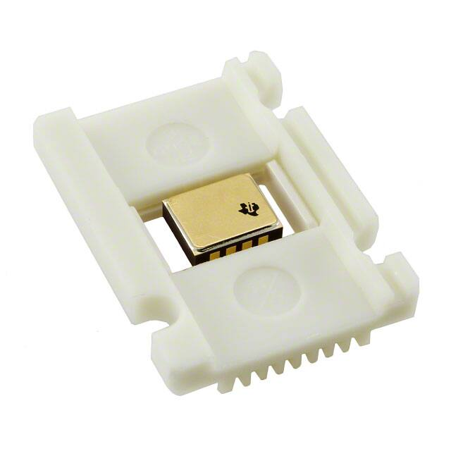


 工商网监
湘ICP备2023018690号
工商网监
湘ICP备2023018690号
