Using the PWR091EVM Dual-Output DC/DC
Analog With PMBus Interface
User's Guide
Literature Number: SLVU638
January 2012
�Contents
1
......................................................................................................................... 7
..................................................................................................... 7
1.2
Features .................................................................................................................. 7
Electrical Performance Specifications ................................................................................... 8
Schematic .......................................................................................................................... 9
Test Setup ........................................................................................................................ 10
4.1
Test and Configuration Software .................................................................................... 10
4.2
Test Equipment ........................................................................................................ 10
4.3
Recommended Test Setup ........................................................................................... 11
4.4
USB Interface Adapter and Cable ................................................................................... 12
4.5
List of Test Points ...................................................................................................... 12
EVM Configuration Using the Fusion GUI ............................................................................. 14
5.1
Configuration Procedure .............................................................................................. 14
Test Procedure .................................................................................................................. 15
6.1
Line/Load Regulation and Efficiency Measurement Procedure .................................................. 15
6.2
Control Loop Gain and Phase Measurement Procedure ......................................................... 15
6.3
Efficiency ................................................................................................................ 16
6.4
Equipment Shutdown .................................................................................................. 16
Performance Data and Typical Characteristic Curves ............................................................ 16
7.1
Efficiency ................................................................................................................ 17
7.2
Load Regulation ........................................................................................................ 18
7.3
Bode Plot ................................................................................................................ 19
7.4
Transient Response ................................................................................................... 20
7.5
Output Ripple ........................................................................................................... 22
7.6
HDRV and Switch Node Voltage .................................................................................... 24
7.7
Turnon Waveform ...................................................................................................... 25
EVM Assembly Drawing and PCB Layout ............................................................................. 26
Bill of Materials ................................................................................................................. 33
Screen Shots .................................................................................................................... 34
10.1 Fusion GUI Screen Shots ............................................................................................. 34
Description
1.1
2
3
4
5
6
7
8
9
10
Typical Applications
SLVU638 – January 2012
Submit Documentation Feedback
Table of Contents
Copyright © 2012, Texas Instruments Incorporated
3
�www.ti.com
List of Figures
PWR091EVM Schematic
2
PWR091EVM Recommended Test Setup ............................................................................. 11
3
Texas Instruments USB-to-GPIO Adapter and Connections ........................................................ 12
4
Tip and Barrel Measurement ............................................................................................. 12
5
Efficiency of 1.2-V Output vs Line and Load ........................................................................... 17
6
Efficiency of 3.3-V Output vs Line and Load ........................................................................... 17
7
Load Regulation of 1.2-V Output ........................................................................................ 18
8
Load Regulation of 3.3-V Output ........................................................................................ 18
9
Bode Plot of 1.2-V Output at 10-A Load ................................................................................ 19
10
Bode Plot of 3.3-V Output at 10-A Load ................................................................................ 19
11
Transient Response of 1.2-V Output at 8 Vin, Transient is 5 A to 11 A to 5 A.................................... 20
12
Transient Response of 1.2-V Output at 12 Vin, Transient is 5 A to 11 A to 5 A .................................. 20
13
Transient Response of 3.3-V Output at 8 Vin, Transient is 5 A to 9 A to 5 A ..................................... 21
14
Transient Response of 3.3-V Output at 12 Vin, Transient is 5 A to 9 A to 5 A.................................... 21
15
Output Ripple and SW Node of 1.2-V Output at 8 Vin, 20-A Output
16
17
18
19
20
21
22
23
24
25
26
27
28
29
30
31
32
33
34
35
36
37
38
39
40
41
42
43
44
45
46
47
4
..................................................................................................
1
..............................................
Output Ripple and SW Node of 1.2-V Output at 12 Vin, 20-A Output ..............................................
Output Ripple and SW Node of 3.3-V Output at 8 Vin, 15-A Output ...............................................
Output Ripple and SW Node of 3.3-V Output at 12 Vin, 15-A Output ..............................................
HDRV and SW Node of 1.2-V Output at 8 Vin, 20-A Output ........................................................
HDRV and SW Node of 1.2-V Output at 12 Vin, 20-A Output .......................................................
HDRV and SW Node of 3.3-V Output at 8-Vin, 15-A Output ........................................................
HDRV and SW Node of 3.3-V Output at 12 Vin, 15-A Output .......................................................
Turnon Waveform of 1.2-V Output at 8-V, 12-V and 14-V Input, 20-A Output ....................................
Turnon Waveform of 1.2-V Output With 0.5-V Prebias, at 8-V, 12-V and 14-V Input, 0-A Output .............
Turnon Waveform of 3.3-V Output at 8-V, 12-V, and 14-V Input, 15-A Output ...................................
Turnon Waveform of 3.3-V Output With 2-V Prebias, at 8-V, 12-V, and 14-V Input, 0-A Output ...............
PWR091EVM Top Layer Assembly Drawing (Top View) ............................................................
PWR091EVM Bottom Assembly Drawing (Bottom View) ............................................................
PWR091EVM Top Copper (Top View) .................................................................................
PWR091EVM Internal Layer 1 (Top View) .............................................................................
PWR091EVM Internal Layer 2 (Top View) .............................................................................
PWR091EVM Bottom Copper (Bottom View) .........................................................................
First Window at Fusion Launch ..........................................................................................
Scan Finds Device Successfully.........................................................................................
Software Launch Continued..............................................................................................
Software Launch Continued..............................................................................................
First Screen After Successful Launch: Configure- Limits & On/Off .................................................
Configure- Other ...........................................................................................................
Configure- All...............................................................................................................
Configure- Limits and On/Off- On/Off Config Pop-up .................................................................
Configure- Limits and On/Off- On/Off Config Pop-up .................................................................
Configure- Other- Iout Cal Gain Change ...............................................................................
Configure- All Config- On/Off Config Pop-up ..........................................................................
Configure- Store User Defaults ..........................................................................................
Change Screens to Other Vout Rail ....................................................................................
Change View Screen to Monitor Screen ...............................................................................
Monitor Screen .............................................................................................................
List of Figures
Copyright © 2012, Texas Instruments Incorporated
9
22
22
23
23
24
24
24
25
25
25
26
26
27
28
29
30
31
32
34
34
34
35
35
36
36
37
37
38
38
39
39
40
41
SLVU638 – January 2012
Submit Documentation Feedback
�www.ti.com
48
System Dashboard ........................................................................................................ 41
49
Display Change on Power Up ........................................................................................... 42
50
Faults Cleared
51
Status Screen .............................................................................................................. 43
52
Import Project / Import Configuration File .............................................................................. 43
53
Store Config To Memory
54
55
56
57
58
59
60
61
.............................................................................................................
.................................................................................................
Data Logging ...............................................................................................................
Data Logging Details ......................................................................................................
Data Log ....................................................................................................................
Data Log File ...............................................................................................................
PMBus Logging ............................................................................................................
PMBus Log Details ........................................................................................................
PMBus Log .................................................................................................................
PMBus Log File ............................................................................................................
SLVU638 – January 2012
Submit Documentation Feedback
List of Figures
Copyright © 2012, Texas Instruments Incorporated
42
44
44
45
45
46
46
47
47
48
5
�www.ti.com
List of Tables
1
PWR091EVM-001 Electrical Performance Specifications ............................................................. 8
2
The Functions of Each Test Points
3
4
5
6
6
.....................................................................................
Key Factory Configuration Parameters .................................................................................
List of Test Points for Loop Response Measurements ...............................................................
List of Test Points for Efficiency Measurements ......................................................................
PWR091 Bill of Materials ................................................................................................
List of Tables
Copyright © 2012, Texas Instruments Incorporated
13
14
15
16
33
SLVU638 – January 2012
Submit Documentation Feedback
�User's Guide
SLVU638 – January 2012
Using the PWR091EVM Dual-Output DC/DC Analog With
PMBus Interface
The PWR091EVM evaluation module uses the TPS40422. The TPS40422 is a dual-channel, synchronous
buck controller that operates from a nominal 4.5-V to 20-V supply. This controller is an analog PWM
controller that allows programming and monitoring via the PMBus interface. It can be used as a dual,
independent output or a dual-phase output controller.
1
Description
The PWR091EVM is designed as a dual-output converter. It uses a nominal 12-V bus to produce a
regulated 1.2-V output at up to 20 A of load current, and a regulated 3.3-V output at up to 15 A of load
current. The PWR091EVM demonstrates the TPS40422 in a typical low-voltage application while providing
a number of test points to evaluate the performance of the TPS40422.
1.1
Typical Applications
•
•
•
•
1.2
Smart power systems
Power supply modules
Communications equipment
Computing equipment
Features
•
•
•
•
Regulated 1.2-V output up to 20-Adc, steady-state output current
Regulated 3.3-V output up to 15-Adc, steady-state output current
Both outputs are marginable and trimmable via the PMBus interface.
– Programmable: UVLO, Soft Start, and Enable via the PMBus interface
– Programmable overcurrent warning and fault limits and programmable response to faults via the
PMBus interface
– Programmable overvoltage warning and fault limit and programmable response to faults via the
PMBus interface
– Programmable high- and low-output margin voltages with a maximum range of +10%, –20% of
nominal output voltage
Convenient test points for probing critical waveforms
SLVU638 – January 2012
Submit Documentation Feedback
Using the PWR091EVM Dual-Output DC/DC Analog With PMBus Interface
Copyright © 2012, Texas Instruments Incorporated
7
�Electrical Performance Specifications
2
www.ti.com
Electrical Performance Specifications
Table 1. PWR091EVM-001 Electrical Performance Specifications
PARAMETER
TEST CONDITIONS
MIN
TYP
MAX
8
UNITS
INPUT CHARACTERISTICS
Voltage range
VIN
12
14
Maximum input current
VIN = 8 V, IO1 = 20 A, IO2 = 15 A
10
15
V
No load input current
VIN = 14 V, IO1 = 0 A, IO2 = 0 A
100
mA
A
OUTPUT CHARACTERISTICS
VOUT1
Output voltage
Output current = 10 A
1.2
V
VOUT2
Output voltage
Output current = 10 A
3.3
V
IOUT1
Output load current
IOUT_min to IOUT_max
0
20
A
IOUT2
Output load current
IOUT_min to IOUT_max
0
15
A
Line regulation: Input voltage = 8 V to 14 V
0.5%
Output voltage regulation
Load regulation: Output current = 0 A to IOUT_max, both
outputs
0.%5
VOUT1
Output voltage ripple
VIN = 12 V, IOUT = 20 A
30
mVpp
VOUT2
Output voltage ripple
VIN = 12 V, IOUT = 15 A
30
mVpp
VOUT1
Output overcurrent
25
A
VOUT2
Output overcurrent
20
A
460
kHz
SYSTEMS CHARACTERISTICS
8
Switching frequency
FSW
VOUT1
Peak efficiency
VIN = 8 V, IO1 = 10 A, VOUT2 disabled, FSW = 300 kHz
92%
VOUT2
Peak efficiency
VIN = 8 V, IO2 = 8.5 A, VOUT1 disabled, FSW = 300 kHz
95%
VOUT1
Full-load efficiency
VIN = 8 V, IO1 = 10 A, VOUT2 disabled, FSW = 300 kHz
90%
VOUT2
Full-load efficiency
VIN = 8 V, IO2 = 8.5 A, VOUT1 disabled, FSW = 300 kHz
93%
Operating temperature
Toper
Using the PWR091EVM Dual-Output DC/DC Analog With PMBus Interface
Copyright © 2012, Texas Instruments Incorporated
25
ºC
SLVU638 – January 2012
Submit Documentation Feedback
�Schematic
www.ti.com
3
Schematic
Figure 1. PWR091EVM Schematic
SLVU638 – January 2012
Submit Documentation Feedback
Using the PWR091EVM Dual-Output DC/DC Analog With PMBus Interface
Copyright © 2012, Texas Instruments Incorporated
9
�Test Setup
www.ti.com
4
Test Setup
4.1
Test and Configuration Software
To change any of the default configuration parameters on the EVM, it is necessary to obtain the TI Fusion
Digital Power Designer software.
4.1.1
Description
The Fusion Digital Power Designer is the graphical user interface (GUI) used to configure and monitor the
Texas Instruments TPS40422 power controller on this evaluation module. The application uses the
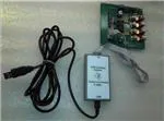
PMBus protocol to communicate with the controller over serial bus by way of a TI USB adapter (see
Figure 3).
4.1.2
Features
Some of the tasks you can perform with the GUI include:
• Turn on or off the power supply output, either through the hardware control line or the PMBus
operation command.
• Monitor real-time data. Items such as input voltage, output voltage, output current, temperature, and
warnings and faults are continuously monitored and displayed by the GUI.
• Configure common operating characteristics such as VOUT trim and margin, UVLO, soft-start time,
warning and fault thresholds, fault response, and ON/OFF.
This software is available for download at http://www.ti.com/tool/fusion_digital_power_designer
4.2
Test Equipment
Voltage Source: The input voltage source VIN must be a 0-V to 14-V variable dc source capable of
supplying 15 Adc. Connect VIN to J5 as shown in Figure 2.
Multimeters: It is recommended to use three separate multimeters as shown in Figure 2. One meter to
measure Vin, one to measure Vout1 and the third to measure Vout2.
Output Load: Two variable electronic loads are recommended for the test setup as shown in Figure 2.
Load 1 must be capable of 25 A at voltages as low as 0.9 V. Load 2 must be capable of 20 A at voltages
as low as 3 V.
Oscilloscope: An oscilloscope is recommended for measuring output noise and ripple. Output ripple must
be measured using a Tip-and-Barrel method or better as shown in Figure 4.The scope must be adjusted
to 20-MHz bandwidth, ac coupling at 50 mV/division, and must be set to 1-µs/division.
Fan: During prolonged operation at high loads, it may be necessary to provide forced air cooling with a
small fan aimed at the EVM. The temperature of the devices on the EVM must be maintained at less than
105°C.
USB-to-GPIO Interface Adapter: A communications adapter is required between the EVM and the host
computer. This EVM was designed to use the Texas Instruments USB-to-GPIO Adapter (see Figure 3).
This adapter can be purchased at http://www.ti.com/tool/usb-to-gpio.
Recommended Wire Gauge: It is recommended that the voltage drop in the load wires does not exceed
0.2 V total in order to keep the voltage at the load above 1 V. See the following table for recommended
wire gauge and length to achieve a voltage drop of no more than 0.2 V at a 20-A load.
10
AWG Gauge
Ohms per Foot
(Ω)
Load Wires Combined Length
(Ft)
Each Wire Length
(Ft)
12
1.59E-3
6.30
3.15
14
2.53E-3
3.96
1.98
16
4.02E-3
2.49
1.25
18
6.39E-3
1.57
0.78
Using the PWR091EVM Dual-Output DC/DC Analog With PMBus Interface
Copyright © 2012, Texas Instruments Incorporated
SLVU638 – January 2012
Submit Documentation Feedback
�Test Setup
www.ti.com
As an example, if AWG 12 wire is used, no more than 3.15 feet of wire must be used between the EVM
and the load.
4.3
Recommended Test Setup
Figure 2. PWR091EVM Recommended Test Setup
SLVU638 – January 2012
Submit Documentation Feedback
Using the PWR091EVM Dual-Output DC/DC Analog With PMBus Interface
Copyright © 2012, Texas Instruments Incorporated
11
�Test Setup
4.4
www.ti.com
USB Interface Adapter and Cable
Figure 3. Texas Instruments USB-to-GPIO Adapter and Connections
Figure 4. Tip and Barrel Measurement
4.5
List of Test Points
12
Using the PWR091EVM Dual-Output DC/DC Analog With PMBus Interface
Copyright © 2012, Texas Instruments Incorporated
SLVU638 – January 2012
Submit Documentation Feedback
�Test Setup
www.ti.com
Table 2. The Functions of Each Test Points
Test Point
Type
Name
Description
TP1
T-H Loop
PGOOD2
TP2
T-H Loop
VIN
TP3
T-H Loop
VOUT1
Tip and barrel point for Vout 1.
TP6
T-H Loop
PGND
Tip and barrel point for Vout 1 return.
TP7
T-H Loop
PGND
General input voltage measurement.
TP11
T-H Loop
VOUT2
Tip and barrel point for Vout 2.
TP13
T-H Loop
AGND
Return for PGOOD signals.
TP14
T-H Loop
PGND
Tip and barrel point for Vout 2 return.
TP15
T-H Loop
PGOOD1
TP16
T-H Loop
BPEXT
TP18
T-H Loop
PREBIAS2
Point to inject Prebias for output 2.
TP19
T-H Loop
PREBIAS1
Point to inject Prebias for output 1.
TP20
T-H Loop
PGND
Return for Prebias 2.
TP21
T-H Loop
PGND
Return for Prebias 1.
TP22
T-H Loop
PGND
Return for BP External.
TP4
SMT
AGND
Return for SYNC signal.
TP8
SMT
INPUT1
Input for control loop measurements for Vout 1.
Power Good signal for Vout 2.
General input voltage measurement.
Power Good signal for Vout 1.
Point to inject BP External.
TP9
SMT
OUTPUT1
Output of Vout 1 for control loop measurements.
TP10
SMT
VOUT2
Output of Vout 2 for control loop measurements.
TP12
SMT
INPUT2
Input for control loop measurements for Vout 2.
TP17
SMT
SYNC
TP5
Copper Dot
VIN
Vin+ measurement point for efficiency of Vout 1.
TP23
Copper Dot
PGND
Vin- measurement point for efficiency of Vout 1.
TP24
Copper Dot
VIN
Vin+ measurement point for efficiency of Vout 2.
TP25
Copper Dot
PGND
Vin- measurement point for efficiency of Vout 2.
TP26
Copper Dot
VOUT2
Vout+ measurement point for efficiency of Vout 2.
TP27
Copper Dot
VOUT1
Vout+ measurement point for efficiency of Vout 1.
SLVU638 – January 2012
Submit Documentation Feedback
Point to inject SYNC signal.
Using the PWR091EVM Dual-Output DC/DC Analog With PMBus Interface
Copyright © 2012, Texas Instruments Incorporated
13
�EVM Configuration Using the Fusion GUI
5
www.ti.com
EVM Configuration Using the Fusion GUI
The TPS40422 on this EVM leaves the factory pre-configured. See Table 3 for a short list of key factory
configuration parameters as obtained from the configuration file.
Table 3. Key Factory Configuration Parameters
Address Hex
0x1B
Address Dec
Part ID
27
TPS40422
General
Cmd ID With Phase
Cmd Code Hex
Encoded Hex
Decoded
Numeric
VIN_OFF
0x36
0xF014
5.00 V
5
Turn OFF voltage
VIN_ON
0x35
0xF01C
7.00 V
7
Turn ON voltage
IOUT_CAL_GAIN
0x38
0x8821
1.0071 mΩ
1.0071
IOUT_CAL_OFFSET
0x39
0xE000
0.0000 A
0
Current offset for GUI readout
IOUT_OC_FAULT_LIMIT
0x46
0xF83C
30.0 A
30
OC fault level
IOUT_OC_FAULT_RESPONSE
0x47
0x3C
Restart Continuously
IOUT_OC_WARN_LIMIT
0x4A
0xF832
25.0 A
25
OC warning level
MFR_04 (VREF_TRIM)
0xD4
0x0000
0.000 V
0
Trim voltage
ON_OFF_CONFIG
0x02
0x02
Mode: Always Converting
OPERATION
0x01
0x00
Unit: Immediate Off; Margin:
None
OT_FAULT_LIMIT
0x4F
0x007D
125 C
125
OT fault level
OT_WARN_LIMIT
0x51
0x0064
100 C
100
OT warn level
TON_RISE
0x61
0xE02B
2.6875 ms
2.6875
Soft-start time
IOUT_CAL_GAIN
0x38
0x8821
1.0071 mΩ
1.0071
IOUT_CAL_OFFSET
0x39
0xE000
0.0000 A
0
Current offset for GUI readout
IOUT_OC_FAULT_LIMIT
0x46
0xF832
25.0 A
25
OC fault level
IOUT_OC_FAULT_RESPONSE
0x47
0x3C
Restart Continuously
IOUT_OC_WARN_LIMIT
0x4A
0xF828
20.0 A
20
OC warning level
MFR_04 (VREF_TRIM)
0xD4
0x0000
0.000 V
0
Trim voltage
ON_OFF_CONFIG
0x02
0x02
Mode: Always Converting
OPERATION
0x01
0x00
Unit: Immediate Off; Margin:
None
OT_FAULT_LIMIT
0x4F
0x007D
125 C
125
OT fault level
OT_WARN_LIMIT
0x51
0x0064
100 C
100
OT warn level
TON_RISE
0x61
0xE02B
2.6875 ms
2.6875
Soft-start time
Vout 1
Comments
Comments
DCR of output inductor
Response to OC fault
Control signal and OPERATION command
not required
Response to turn OFF trigger
Vout 2
Comments
DCR of output inductor
Response to OC fault
Control signal and OPERATION command
not required
Response to turn OFF trigger
If it is desired to configure the EVM to settings other than the factory settings shown in Table 3, the TI
Fusion Digital Power Designer software can be used for reconfiguration. It is necessary to have input
voltage applied to the EVM prior to launching the software so that the TPS40422 may respond to the GUI
and the GUI can recognize the TPS40422. The default configuration for the EVM is to start converting at
an input voltage of 7 V; therefore, to avoid any converter activity during configuration, an input voltage less
than 7 V must be applied. An input voltage of 5 V is recommended.
5.1
Configuration Procedure
1.
2.
3.
4.
14
Adjust the input supply to provide 5 Vdc, current limited to 1 A.
Apply the input voltage to the EVM. See Figure 2 and Figure 3 for connections and test setup.
Launch the Fusion GUI software. See the screen shots in Section 10 for more information.
Configure the EVM operating parameters as desired.
Using the PWR091EVM Dual-Output DC/DC Analog With PMBus Interface
Copyright © 2012, Texas Instruments Incorporated
SLVU638 – January 2012
Submit Documentation Feedback
�Test Procedure
www.ti.com
NOTE: The IOUT_CAL_GAIN parameter is used by the TPS40422 in the calculation of output
current level, and this number is the dc resistance of the output inductor. Although this
number can be reconfigured, a number entry that does not match the actual DCR of the
inductor on the EVM will result in current reporting inaccuracy. This also affects OC Fault
and OC Warn performance.
The TON_RISE parameter may affect proper start-up if the rise time and output capacitance
bank result in a current that exceeds the OC Fault level. The start-up surge current in the
output capacitance bank is added to the load current, so the sum of these two currents must
be less than the OC Fault level for proper start-up.
6
Test Procedure
6.1
Line/Load Regulation and Efficiency Measurement Procedure
1. Set up the EVM as described in Section 4.3 and Figure 2.
2. Ensure that both electronic loads are set to draw 0 Adc.
3. Increase Vin from 0 V to 12 V using DMM1 to measure input voltage.
4. Use DMM2 to measure output voltage Vout1.
5. Vary the load from 0 Adc to 20 Adc. Vout1 must remain in regulation as defined in Table 1.
6. Vary Vin from 8 V to 14 V. Vout1 must remain in regulation as defined in Table 1.
7. Decrease the load to 0 A.
8. Use DMM3 to measure output voltage Vout2.
9. Vary the load from 0 Adc to 15 Adc. Vout1 must remain in regulation as defined in Table 1.
10. Vary Vin from 8 V to 14 V. Vout2 must remain in regulation as defined in Table 1.
11. Decrease the load to 0 A.
12. Decrease Vin to 0 V.
6.2
Control Loop Gain and Phase Measurement Procedure
The PWR091EVM includes a 49.9-Ω series resistor in the feedback loop for both Vout1 and Vout2. These
resistors are used for loop response analysis and are accessible at the test points TP8 and TP9 for Vout1,
and TP10 and TP12 for Vout2. Those test points must be used during loop response measurements as
the injection points for the loop perturbation. See the short descriptions listed in Table 4.
Table 4. List of Test Points for Loop Response Measurements
Test Point
Node Name
Description
Comment
Input to feedback divider of
Vout1
The amplitude of the perturbation at this node must be limited to
less than 100 mV.
Resulting output of Vout1
Bode plot data can be measured by a network analyzer as
TP9/TP8.
TP8
INPUT1
TP9
OUTPUT1
TP12
INPUT2
Input to feedback divider of
Vout2
The amplitude of the perturbation at this node must be limited to
less than 100mV.
TP10
VOUT2
Resulting output of Vout2
Bode plot data can be measured by a network analyzer as
TP10/TP12.
Measure only one output at a time with the following procedure:
1. Set up the EVM as described in Section 4.3 and Figure 2.
2. For Vout1, connect the network analyzer’s isolation transformer from TP8 to TP9.
3. Connect the input signal measurement probe to TP8. Connect output signal measurement probe to
TP9.
4. Connect the ground leads of both probe channels to TP4.
5. On the network analyzer, measure the Bode plot data as TP9/TP8 (Out/In). The frequency sweep must
SLVU638 – January 2012
Submit Documentation Feedback
Using the PWR091EVM Dual-Output DC/DC Analog With PMBus Interface
Copyright © 2012, Texas Instruments Incorporated
15
�Performance Data and Typical Characteristic Curves
www.ti.com
be limited to less than the switching frequency divided by 2 (Fsw/2).
6. For Vout2, connect the network analyzer’s isolation transformer from TP12 to TP10.
7. Connect the input signal measurement probe to TP12. Connect output signal measurement probe to
TP10.
8. Connect the ground leads of both probe channels to TP4.
9. On the network analyzer, measure the Bode plot data as TP10/TP12 (Out/In). The frequency sweep
must be limited to less than the switching frequency divided by 2 (Fsw/2).
10. Disconnect the isolation transformer from the Bode plot test points before making other
measurements, because the signal injection into the feedback loop may interfere with the accuracy of
other measurements.
6.3
Efficiency
To measure the efficiency of the power train on the EVM, it is important to measure the voltages at the
correct location. This is necessary because otherwise the measurements will include losses in efficiency
that are not related to the power train itself. Losses incurred by the voltage drop in the copper traces and
in the input and output connectors are not related to the efficiency of the power train, and they must not be
included in efficiency measurements.
When measuring the efficiency of Vout1, Vout2 must be disabled by the user via the Fusion GUI.
Likewise, when measuring the efficiency of Vout2, Vout1 must be disabled by the user. See the list in
Table 5 for the proper locations to measure efficiency.
Table 5. List of Test Points for Efficiency Measurements
Test Point
Node Name
Description
Comment
TP5
VIN
Measurement point for VIN +VE
Copper dot at high-side FET drain
TP23
PGND
Measurement point for VIN –VE
Copper dot at low-side FET source
TP27
VOUT1
Measurement point for VOUT1 +VE
Copper dot at output inductor, dc side
TP23
PGND
Measurement point for VOUT1 –VE
Copper dot at low-side FET source
TP24
VIN
Measurement point for VIN +VE
Copper dot at high-side FET drain
TP25
PGND
Measurement point for VIN –VE
Copper dot at low-side FET source
TP26
VOUT2
Measurement point for VOUT2 +VE
Copper dot at output inductor, dc side
TP25
PGND
Measurement point for VOUT2 –VE
Copper dot at low-side FET source
Input current can be measured at any point in the input wires, and output current can be measured
anywhere in the output wires of the output being measured. Using these measurement points result in
efficiency measurements that do not include losses due to the connectors and PCB traces.
6.4
Equipment Shutdown
1.
2.
3.
4.
7
Reduce the load current on both outputs to 0 A.
Reduce input voltage to 0 V.
Shut down the external fan if in use.
Shut down equipment.
Performance Data and Typical Characteristic Curves
Figure 5 through Figure 25 present typical performance curves for the PWR091EVM.
16
Using the PWR091EVM Dual-Output DC/DC Analog With PMBus Interface
Copyright © 2012, Texas Instruments Incorporated
SLVU638 – January 2012
Submit Documentation Feedback
�Performance Data and Typical Characteristic Curves
www.ti.com
7.1
Efficiency
100
VO = 1.2 V,
98 F
SW = 300 kHz
96
VI = 12 V
VI = 8 V
94
VI = 14 V
92
Efficiency - %
90
88
86
84
82
80
78
76
74
72
70
0
1
2
3
4
5
6
7
8
9 10 11 12 13 14 15 16 17 18 19 20
IO - Output Current - A
Figure 5. Efficiency of 1.2-V Output vs Line and Load
100
VO = 3.3 V,
FSW = 300 kHz
98
96
VI = 8 V
VI = 12 V
VI = 14 V
94
Efficiency - %
92
90
88
86
84
82
80
78
76
74
72
70
0
1
2
3
4
5
6
7
8
9
10
IO - Output Current - A
11
12
13
14
15
Figure 6. Efficiency of 3.3-V Output vs Line and Load
SLVU638 – January 2012
Submit Documentation Feedback
Using the PWR091EVM Dual-Output DC/DC Analog With PMBus Interface
Copyright © 2012, Texas Instruments Incorporated
17
�Performance Data and Typical Characteristic Curves
7.2
www.ti.com
Load Regulation
1.2016
1.2015
VI = 8 V
VO - Output Voltage - V
1.2014
VI = 14 V
1.2013
1.2012
VI = 12 V
1.2011
1.2010
1.2009
1.2008
1.2007
1.2006
0
1
2
3
4
5
6
7
8
9 10 11 12 13 14 15 16 17 18 19 20
IO - Output Current - A
Figure 7. Load Regulation of 1.2-V Output
3.330
3.329
VO - Output Voltage - V
3.328
VI = 14 V
VI = 12 V
3.327
3.326
VI = 8 V
3.325
3.324
3.323
3.322
0
1
2
3
4
5
6
7
8
9
10
IO - Output Current - A
11
12
13
14
15
Figure 8. Load Regulation of 3.3-V Output
18
Using the PWR091EVM Dual-Output DC/DC Analog With PMBus Interface
Copyright © 2012, Texas Instruments Incorporated
SLVU638 – January 2012
Submit Documentation Feedback
�Performance Data and Typical Characteristic Curves
www.ti.com
Bode Plot
70
Gain - dB
60
140
8 V Phase
12 V Phase
14 V Phase
120
50
100
40
80
30
60
20
40
10
8 V Gain
12 V Gain
14 V Gain
20
0
Phase (Deg)
7.3
0
-10
-20
-20
-40
-30
100
1k
10k
-60
100k
f - Frequency - Hz
Figure 9. Bode Plot of 1.2-V Output at 10-A Load
70
120
50
100
40
80
30
60
20
8 V Gain
12 V Gain
14 V Gain
40
10
20
0
0
-10
-20
-20
-40
-30
100
1k
10k
Phase (Deg)
Gain - dB
60
140
8 V Phase
12 V Phase
14 V Phase
-60
100k
f - Frequency - Hz
Figure 10. Bode Plot of 3.3-V Output at 10-A Load
SLVU638 – January 2012
Submit Documentation Feedback
Using the PWR091EVM Dual-Output DC/DC Analog With PMBus Interface
Copyright © 2012, Texas Instruments Incorporated
19
�Performance Data and Typical Characteristic Curves
7.4
www.ti.com
Transient Response
Ch1 = Vout1 at 50mV/division, Ch2 = Iout1 at 5A/division
Figure 11. Transient Response of 1.2-V Output at 8 Vin, Transient is 5 A to 11 A to 5 A
Ch1 = Vout1 at 50mV/division, Ch2 = Iout1 at 5A/division
Figure 12. Transient Response of 1.2-V Output at 12 Vin, Transient is 5 A to 11 A to 5 A
20
Using the PWR091EVM Dual-Output DC/DC Analog With PMBus Interface
Copyright © 2012, Texas Instruments Incorporated
SLVU638 – January 2012
Submit Documentation Feedback
�Performance Data and Typical Characteristic Curves
www.ti.com
Ch1 = Vout2 at 20mV/division, Ch2 = Iout2 at 5A/division
Figure 13. Transient Response of 3.3-V Output at 8 Vin, Transient is 5 A to 9 A to 5 A
Ch1 = Vout2 at 20mV/division, Ch2 = Iout2 at 5A/division
Figure 14. Transient Response of 3.3-V Output at 12 Vin, Transient is 5 A to 9 A to 5 A
SLVU638 – January 2012
Submit Documentation Feedback
Using the PWR091EVM Dual-Output DC/DC Analog With PMBus Interface
Copyright © 2012, Texas Instruments Incorporated
21
�Performance Data and Typical Characteristic Curves
7.5
www.ti.com
Output Ripple
Ch1 = Vout1 at 20mV/division, Ch2 = SW Node at 10V/division
Figure 15. Output Ripple and SW Node of 1.2-V Output at 8 Vin, 20-A Output
Ch1 = Vout1 at 20mV/division, Ch2 = SW Node at 10V/division
Figure 16. Output Ripple and SW Node of 1.2-V Output at 12 Vin, 20-A Output
22
Using the PWR091EVM Dual-Output DC/DC Analog With PMBus Interface
Copyright © 2012, Texas Instruments Incorporated
SLVU638 – January 2012
Submit Documentation Feedback
�Performance Data and Typical Characteristic Curves
www.ti.com
Ch1 = Vout2 at 20mV/division, Ch2 = SW Node at 10V/division
Figure 17. Output Ripple and SW Node of 3.3-V Output at 8 Vin, 15-A Output
Ch1 = Vout2 at 20mV/division, Ch2 = SW Node at 10V/division
Figure 18. Output Ripple and SW Node of 3.3-V Output at 12 Vin, 15-A Output
SLVU638 – January 2012
Submit Documentation Feedback
Using the PWR091EVM Dual-Output DC/DC Analog With PMBus Interface
Copyright © 2012, Texas Instruments Incorporated
23
�Performance Data and Typical Characteristic Curves
7.6
www.ti.com
HDRV and Switch Node Voltage
Ch1 = SW Node at 5 V/division, Ch2 = HDRV at 5 V/division
Figure 19. HDRV and SW Node of 1.2-V Output at 8 Vin, 20-A Output
Ch1 = SW Node at 5 V/division, Ch2 = HDRV at 10 V/division
Figure 20. HDRV and SW Node of 1.2-V Output at 12 Vin, 20-A Output
Ch1 = SW Node at 5 V/division, Ch2 = HDRV at 5 V/division
Figure 21. HDRV and SW Node of 3.3-V Output at 8-Vin, 15-A Output
24
Using the PWR091EVM Dual-Output DC/DC Analog With PMBus Interface
Copyright © 2012, Texas Instruments Incorporated
SLVU638 – January 2012
Submit Documentation Feedback
�Performance Data and Typical Characteristic Curves
www.ti.com
Ch1 = SW Node at 5 V/division, Ch2 = HDRV at 10 V/division
Figure 22. HDRV and SW Node of 3.3-V Output at 12 Vin, 15-A Output
7.7
Turnon Waveform
Ch1 = Vout1 at 200 mV/division, Ch2 = Iout1 at 5 A/division, Ch3 = Vin at 5 V/division Ch2 (Iout) Inverted to better
display V and I.
Figure 23. Turnon Waveform of 1.2-V Output at 8-V, 12-V and 14-V Input, 20-A Output
Ch1 = Vout1 at 200 mV/division, Ch3 = Vin at 5 V/division
Figure 24. Turnon Waveform of 1.2-V Output With 0.5-V Prebias, at 8-V, 12-V and 14-V Input, 0-A Output
SLVU638 – January 2012
Submit Documentation Feedback
Using the PWR091EVM Dual-Output DC/DC Analog With PMBus Interface
Copyright © 2012, Texas Instruments Incorporated
25
�EVM Assembly Drawing and PCB Layout
www.ti.com
Ch1 = Vout2 at 500 mV/division, Ch2 = Iout2 at 5 A/division, Ch3 = Vin at 5 V/division Ch2 (Iout) Inverted to better
display V and I.
Figure 25. Turnon Waveform of 3.3-V Output at 8-V, 12-V, and 14-V Input, 15-A Output
Ch1 = Vout1 at 500 mV/division, Ch3 = Vin at 5 V/division
Figure 26. Turnon Waveform of 3.3-V Output With 2-V Prebias, at 8-V, 12-V, and 14-V Input, 0-A Output
8
EVM Assembly Drawing and PCB Layout
Figure 27 through Figure 32 show the design of the PWR091EVM printed-circuit board (PCB).
26
Using the PWR091EVM Dual-Output DC/DC Analog With PMBus Interface
Copyright © 2012, Texas Instruments Incorporated
SLVU638 – January 2012
Submit Documentation Feedback
�EVM Assembly Drawing and PCB Layout
www.ti.com
Figure 27. PWR091EVM Top Layer Assembly Drawing (Top View)
SLVU638 – January 2012
Submit Documentation Feedback
Using the PWR091EVM Dual-Output DC/DC Analog With PMBus Interface
Copyright © 2012, Texas Instruments Incorporated
27
�EVM Assembly Drawing and PCB Layout
www.ti.com
Figure 28. PWR091EVM Bottom Assembly Drawing (Bottom View)
28
Using the PWR091EVM Dual-Output DC/DC Analog With PMBus Interface
Copyright © 2012, Texas Instruments Incorporated
SLVU638 – January 2012
Submit Documentation Feedback
�EVM Assembly Drawing and PCB Layout
www.ti.com
Figure 29. PWR091EVM Top Copper (Top View)
SLVU638 – January 2012
Submit Documentation Feedback
Using the PWR091EVM Dual-Output DC/DC Analog With PMBus Interface
Copyright © 2012, Texas Instruments Incorporated
29
�EVM Assembly Drawing and PCB Layout
www.ti.com
Figure 30. PWR091EVM Internal Layer 1 (Top View)
30
Using the PWR091EVM Dual-Output DC/DC Analog With PMBus Interface
Copyright © 2012, Texas Instruments Incorporated
SLVU638 – January 2012
Submit Documentation Feedback
�EVM Assembly Drawing and PCB Layout
www.ti.com
Figure 31. PWR091EVM Internal Layer 2 (Top View)
SLVU638 – January 2012
Submit Documentation Feedback
Using the PWR091EVM Dual-Output DC/DC Analog With PMBus Interface
Copyright © 2012, Texas Instruments Incorporated
31
�EVM Assembly Drawing and PCB Layout
www.ti.com
Figure 32. PWR091EVM Bottom Copper (Bottom View)
32
Using the PWR091EVM Dual-Output DC/DC Analog With PMBus Interface
Copyright © 2012, Texas Instruments Incorporated
SLVU638 – January 2012
Submit Documentation Feedback
�Bill of Materials
www.ti.com
9
Bill of Materials
The EVM components list according to the schematic shown in .
Table 6. PWR091 Bill of Materials
Qty
Reference Designator
Description
Manufacturer
Part Number
2
C23 C27
0.47uF, Ceramic, 16V, X5R, 10%, 0402
STD
STD
3
C1 C5 C9
0.1uF, Ceramic, 50V, X7R, 10%, 0603
STD
STD
3
C10-12
1.0uF, Ceramic, 25V, X7R, 10%, 0603
STD
STD
2
C21 C25
1.2nF, Ceramic, 50V, X7R, 10%, 0603
STD
STD
2
C24 C33
470pF, Ceramic, 50V, X7R, 10%, 0603
STD
STD
2
C26 C22
120pF, Ceramic, 50V, NP0, 5%, 0603
STD
STD
6
C31-32 C30 C34-35 C37
1000pF, Ceramic, 50V, X7R, 10%, 0603
STD
STD
4
C19-20 C42-43
22uF, Ceramic, 6.3V, X5R, 20%, 0805
STD
STD
2
C38-39
0.1uF, Ceramic, 6.3V, X5R, 20%, 0805
STD
STD
9
C2-4 C6-8 C36 C40-41
22uF, Ceramic, 25V, X5R, 20%, 1210
STD
STD
6
C18 C15 C44-47
100uF, Ceramic, 6.3V, X5R, 20%, 1210
STD
STD
2
C28-29
330uF, Electrolytic, Aluminum, 25V, 200mohm, 270mArms, 0.406 x 0.406
Panasonic
EEE-TK1E331UP
4
C13-14 C16-17
330uF, Polymer Cap, 330uF, 6.3V, 0.015 Ohms, 20%, 7343(D)
Kemet
T520D337M006ATE015
4
J4 J6-8
33457, Lug, Solderless, #10 - #10-12 AWG, Copper/Tin, Uninsulated, 0.375 x1.00"
Std
CX35-36-CY
2
D1-2
MBRS340, Diode, Schottky, 3A, 40V, SMC
Fairchild
MBRS340
2
J1-2
PEC02SAAN, Header, Male 2-pin, 100mil spacing,, 0.100" x 2
Sullins
PEC02SAAN
1
J3
AWHW10G, Header, Male 2x5-pin, 100mil spacing, 0.100" x 5 X 2
Assmann
AWHW10G-0202-T-R
2
L1-2
820nH, Inductor, SMT, 27A, Shielded, 20%, 0.9mOhm, 0.512" x 0.571"
Wurth
744355182
2
R1 R4
5.1, Resistor, Chip, 1/10W, 1%, 0603
STD
STD
1
R3
0, Resistor, Chip, 1/10W, 1%, 0603
STD
STD
1
R2
0, Resistor, Chip, 1/10W, 5%, 0603
STD
STD
2
R5-6
2.0k, Resistor, Chip, 1/10W, 1%, 0603
STD
STD
0
R7 R16 R21-23 R34
Open, Resistor, Chip, 1/10W, 1%, 0603
STD
STD
3
R12 R13 R38
47.5k, Resistor, Chip, 1/10W, 1%, 0603
STD
STD
2
R8-9
36.5k, Resistor, Chip, 1/10W, 1%, 0603
STD
STD
11
R17 R18 R20 R24-26 R28-30 R33
R36
10, Resistor, Chip, 1/10W, 1%, 0603
STD
STD
1
R10
40.2k, Resistor, Chip, 1/10W, 1%, 0603
STD
STD
3
R11 R27 R31
49.9, Resistor, Chip, 1/10W, 1%, 0603
STD
STD
2
R15 R32
20k, Resistor, Chip, 1/10W, 1%, 0603
STD
STD
1
R35
10.5k, Resistor, Chip, 1/10W, 1%, 0603
STD
STD
3
R19 R37 R40
10.0k, Resistor, Chip, 1/10W, 1%, 0603
STD
STD
2
R14 R39
4.75k, Resistor, Chip, 1/10W, 1%, 0603
STD
STD
1
J5
ED120/2DS, Terminal Block, 2-pin, 15-A, 5.1mm, 0.40" x 0.35"
OST
ED120/2DS
1
U1
TPS40422RHA, IC, PMBUS synchronous buck controller, QFN-40
TI
TPS40422RHA
2
Q1-2
CSD87350Q5D, MOSFET, Dual N-Chan, 30-V, 30-A, QFN-8 POWER
TI
CSD87350Q5D
2
Q3-4
MMBT3904, Bipolar, NPN, 40V, 200mA, 200mW, SC-75
On Semi
MMBT3904TT1G
1
PCB
PCB, FR-4, 0.062, 2oz Copper all layers., 4.00" x 4.00"
STD
STD
SLVU638 – January 2012
Submit Documentation Feedback
Using the PWR091EVM Dual-Output DC/DC Analog With PMBus Interface
Copyright © 2012, Texas Instruments Incorporated
33
�Screen Shots
10
www.ti.com
Screen Shots
10.1 Fusion GUI Screen Shots
Figure 33. First Window at Fusion Launch
Device Found
Figure 34. Scan Finds Device Successfully
Figure 35. Software Launch Continued
34
Using the PWR091EVM Dual-Output DC/DC Analog With PMBus Interface
Copyright © 2012, Texas Instruments Incorporated
SLVU638 – January 2012
Submit Documentation Feedback
�Screen Shots
www.ti.com
Figure 36. Software Launch Continued
Use this screen to configure (Figure 37):
• OC Fault and OC Warn
• OT Fault and OT Warn
• Power Good Limits
• Fault response
• UVLO
• On/Off Config
• Soft Start time
• Margin voltage
Figure 37. First Screen After Successful Launch: Configure- Limits & On/Off
Use this screen to configure (Figure 38) :
• Vref Trim
SLVU638 – January 2012
Submit Documentation Feedback
Using the PWR091EVM Dual-Output DC/DC Analog With PMBus Interface
Copyright © 2012, Texas Instruments Incorporated
35
�Screen Shots
•
www.ti.com
Iout Cal Gain (DCR of output choke)
Figure 38. Configure- Other
Use this screen to configure all of the configurable parameters (Figure 39). The screen also shows other
details like hexadecimal (hex) encoding.
Figure 39. Configure- All
Changing the On/Off Config prompts a pop-up window with details of the options Figure 40).
36
Using the PWR091EVM Dual-Output DC/DC Analog With PMBus Interface
Copyright © 2012, Texas Instruments Incorporated
SLVU638 – January 2012
Submit Documentation Feedback
�Screen Shots
www.ti.com
Figure 40. Configure- Limits and On/Off- On/Off Config Pop-up
After a change is selected, orange U icon is displayed to offer Undo Change option. Change is not
retained until either Write to Hardware or Store User Defaults is selected. When Write to Hardware is
selected, change is committed to volatile memory and defaults back to previous setting on input power
cycle. When Store User Defaults is selected, change is committed to nonvolatile memory and becomes
the new default (Figure 41).
Figure 41. Configure- Limits and On/Off- On/Off Config Pop-up
SLVU638 – January 2012
Submit Documentation Feedback
Using the PWR091EVM Dual-Output DC/DC Analog With PMBus Interface
Copyright © 2012, Texas Instruments Incorporated
37
�Screen Shots
www.ti.com
The Iout Cal Gain can be typed in or scrolled to a new value. The range for Iout Cal Gain is 0.244 mΩ to
15.5 mΩ and the resolution step is 30.5 µΩ. If a value is typed in that is between the available discrete
steps, the typed-in value does not change but the nearest discrete step is retained. The actual step is
displayed on relaunch of the Fusion GUI (Figure 42).
Figure 42. Configure- Other- Iout Cal Gain Change
On/Off Config can also be configured from the All Config screen, and the same process applies
(Figure 43).
Figure 43. Configure- All Config- On/Off Config Pop-up
38
Using the PWR091EVM Dual-Output DC/DC Analog With PMBus Interface
Copyright © 2012, Texas Instruments Incorporated
SLVU638 – January 2012
Submit Documentation Feedback
�Screen Shots
www.ti.com
After making changes to one or more configurable parameters, the changes can be committed to
nonvolatile memory by selecting Store User Defaults. This action prompts a confirm selection pop-up, and
if confirmed, the changes are committed to nonvolatile memory (Figure 44).
Figure 44. Configure- Store User Defaults
A scroll-down menu in the upper right corner can be selected to change the view screens to one output
rail or the other(Figure 45).
Figure 45. Change Screens to Other Vout Rail
SLVU638 – January 2012
Submit Documentation Feedback
Using the PWR091EVM Dual-Output DC/DC Analog With PMBus Interface
Copyright © 2012, Texas Instruments Incorporated
39
�Screen Shots
www.ti.com
In the lower left corner, the different view screens can be changed. The view screens can be changed
between Configure, Monitor and Status as needed (Figure 46).
Figure 46. Change View Screen to Monitor Screen
When the Monitor screen is selected (Figure 47), the screen changes to display real-time data of the
parameters that are measured by the controller. This screen provides access to:
• Graphs of Vout, Iout, Temperature, and Pout. As shown, Pout display is turned off.
• Start/Stop Polling which turns on or off the real-time display of data.
• Quick access to On/Off config
• Control pin activation, and OPERATION command. As shown, because the device is configured for
Always Converting, these radio buttons are either grayed-out or have no effect.
• Margin control.
• PMBus log which displays activity on the PMBus.
• Tips & Hints which displays additional information when the cursor is hovered over configurable
parameters.
As shown, when the EVM is still off due to UVLO, no output voltage or current is displayed.
At first GUI launch, Faults may occur due to communications during power up. These faults can be
cleared once the device is enabled.
40
Using the PWR091EVM Dual-Output DC/DC Analog With PMBus Interface
Copyright © 2012, Texas Instruments Incorporated
SLVU638 – January 2012
Submit Documentation Feedback
�Screen Shots
www.ti.com
Figure 47. Monitor Screen
Selecting System Dashboard from mid-left screen adds a new window which displays system-level
information (Figure 48).
Figure 48. System Dashboard
SLVU638 – January 2012
Submit Documentation Feedback
Using the PWR091EVM Dual-Output DC/DC Analog With PMBus Interface
Copyright © 2012, Texas Instruments Incorporated
41
�Screen Shots
www.ti.com
When the EVM starts converting power, the Vout graph changes scale to display both the zero and Vout
level. Only one rail can be displayed on the graphs at any time, but the other rail voltage, current, power,
and temperature are displayed in the upper left window. Once the EVM is converting and clear of any
faults, selecting Clear Faults clears any prior fault flags (Figure 49).
Figure 49. Display Change on Power Up
Selecting Clear Faults clears any prior fault flags. Scrolling time window of Vout still shows the turnon
event (Figure 50).
Figure 50. Faults Cleared
42
Using the PWR091EVM Dual-Output DC/DC Analog With PMBus Interface
Copyright © 2012, Texas Instruments Incorporated
SLVU638 – January 2012
Submit Documentation Feedback
�Screen Shots
www.ti.com
Selecting Status from lower left corner shows the status of the controller (Figure 51).
Figure 51. Status Screen
Selecting the pull-down menu File- Import Project from the upper left menu bar can be used to configure
all parameters in the device at once with a desired configuration, or even revert back to a known-good
configuration. This action results in a browse-type sequence where the desired config file can be located
and loaded (Figure 52).
Figure 52. Import Project / Import Configuration File
SLVU638 – January 2012
Submit Documentation Feedback
Using the PWR091EVM Dual-Output DC/DC Analog With PMBus Interface
Copyright © 2012, Texas Instruments Incorporated
43
�Screen Shots
www.ti.com
Selecting Store User Configuration to Flash Memory from the Device pull-down menu has the same
functionality as the Store User Defaults button from within the Configure screen. It results in committing
the current configuration to nonvolatile memory (Figure 53).
Figure 53. Store Config To Memory
Selecting Data Logging (Figure 54) from the Tools drop-down menu enables the logging of common
operating values such as Vout, Iout, and Temperature for both output rails. The user is prompted to select
a location for the file to be stored as well as the type of file. See next screen (Figure 55).
Figure 54. Data Logging
44
Using the PWR091EVM Dual-Output DC/DC Analog With PMBus Interface
Copyright © 2012, Texas Instruments Incorporated
SLVU638 – January 2012
Submit Documentation Feedback
�Screen Shots
www.ti.com
Select the storage location for the file and the type of file. As shown (Figure 55), the file will be a CSV file
to be stored in the directory path shown. Logging begins when the Start Data Logging button is selected,
and stops when it is reselected (as Stop Data Logging).
Figure 55. Data Logging Details
Data is stored in a CSV file, with date-stamp name (Figure 56).
Figure 56. Data Log
Common contents of the data log. As shown (Figure 57), the UUT had been disabled, and both rails were
off .
SLVU638 – January 2012
Submit Documentation Feedback
Using the PWR091EVM Dual-Output DC/DC Analog With PMBus Interface
Copyright © 2012, Texas Instruments Incorporated
45
�Screen Shots
www.ti.com
Figure 57. Data Log File
Selecting PMBus Logging (Figure 58) from the Tools drop-down menu enables the logging of all PMBus
activity. This includes communications traffic for each polling loop between the GUI and the device. It also
includes common operating values such as Vout, Iout, and Temperature for both output rails. The user is
prompted to select a location for the file to be stored. See next screen (Figure 59).
Figure 58. PMBus Logging
46
Using the PWR091EVM Dual-Output DC/DC Analog With PMBus Interface
Copyright © 2012, Texas Instruments Incorporated
SLVU638 – January 2012
Submit Documentation Feedback
�Screen Shots
www.ti.com
Select the storage location for the file and the type of file. As shown (Figure 59), the file is a CSV file to be
stored in the directory path shown. Logging begins when the Start Logging button is selected, and stops
when it is reselected (as Stop Logging). This file can rapidly grow in size, so caution is advised when
using this function.
Figure 59. PMBus Log Details
Data is stored in a CSV file, with date-stamp name (Figure 60).
Figure 60. PMBus Log
Common contents of the PMBus log. As shown (Figure 61), the UUT had been disabled, and both rails
were off.
SLVU638 – January 2012
Submit Documentation Feedback
Using the PWR091EVM Dual-Output DC/DC Analog With PMBus Interface
Copyright © 2012, Texas Instruments Incorporated
47
�Screen Shots
www.ti.com
Figure 61. PMBus Log File
48
Using the PWR091EVM Dual-Output DC/DC Analog With PMBus Interface
Copyright © 2012, Texas Instruments Incorporated
SLVU638 – January 2012
Submit Documentation Feedback
�Evaluation Board/Kit Important Notice
Texas Instruments (TI) provides the enclosed product(s) under the following conditions:
This evaluation board/kit is intended for use for ENGINEERING DEVELOPMENT, DEMONSTRATION, OR EVALUATION
PURPOSES ONLY and is not considered by TI to be a finished end-product fit for general consumer use. Persons handling the
product(s) must have electronics training and observe good engineering practice standards. As such, the goods being provided are
not intended to be complete in terms of required design-, marketing-, and/or manufacturing-related protective considerations,
including product safety and environmental measures typically found in end products that incorporate such semiconductor
components or circuit boards. This evaluation board/kit does not fall within the scope of the European Union directives regarding
electromagnetic compatibility, restricted substances (RoHS), recycling (WEEE), FCC, CE or UL, and therefore may not meet the
technical requirements of these directives or other related directives.
Should this evaluation board/kit not meet the specifications indicated in the User’s Guide, the board/kit may be returned within 30
days from the date of delivery for a full refund. THE FOREGOING WARRANTY IS THE EXCLUSIVE WARRANTY MADE BY
SELLER TO BUYER AND IS IN LIEU OF ALL OTHER WARRANTIES, EXPRESSED, IMPLIED, OR STATUTORY, INCLUDING
ANY WARRANTY OF MERCHANTABILITY OR FITNESS FOR ANY PARTICULAR PURPOSE.
The user assumes all responsibility and liability for proper and safe handling of the goods. Further, the user indemnifies TI from all
claims arising from the handling or use of the goods. Due to the open construction of the product, it is the user’s responsibility to
take any and all appropriate precautions with regard to electrostatic discharge.
EXCEPT TO THE EXTENT OF THE INDEMNITY SET FORTH ABOVE, NEITHER PARTY SHALL BE LIABLE TO THE OTHER
FOR ANY INDIRECT, SPECIAL, INCIDENTAL, OR CONSEQUENTIAL DAMAGES.
TI currently deals with a variety of customers for products, and therefore our arrangement with the user is not exclusive.
TI assumes no liability for applications assistance, customer product design, software performance, or infringement of
patents or services described herein.
Please read the User’s Guide and, specifically, the Warnings and Restrictions notice in the User’s Guide prior to handling the
product. This notice contains important safety information about temperatures and voltages. For additional information on TI’s
environmental and/or safety programs, please contact the TI application engineer or visit www.ti.com/esh.
No license is granted under any patent right or other intellectual property right of TI covering or relating to any machine, process, or
combination in which such TI products or services might be or are used.
FCC Warning
This evaluation board/kit is intended for use for ENGINEERING DEVELOPMENT, DEMONSTRATION, OR EVALUATION
PURPOSES ONLY and is not considered by TI to be a finished end-product fit for general consumer use. It generates, uses, and
can radiate radio frequency energy and has not been tested for compliance with the limits of computing devices pursuant to part 15
of FCC rules, which are designed to provide reasonable protection against radio frequency interference. Operation of this
equipment in other environments may cause interference with radio communications, in which case the user at his own expense
will be required to take whatever measures may be required to correct this interference.
EVM Warnings and Restrictions
It is important to operate this EVM within the input voltage range of 8 V to 14 V and the output voltage range of 1.2 V to 3.3 V .
Exceeding the specified input range may cause unexpected operation and/or irreversible damage to the EVM. If there are
questions concerning the input range, please contact a TI field representative prior to connecting the input power.
Applying loads outside of the specified output range may result in unintended operation and/or possible permanent damage to the
EVM. Please consult the EVM User's Guide prior to connecting any load to the EVM output. If there is uncertainty as to the load
specification, please contact a TI field representative.
During normal operation, some circuit components may have case temperatures greater than 60° C. The EVM is designed to
operate properly with certain components above 60° C as long as the input and output ranges are maintained. These components
include but are not limited to linear regulators, switching transistors, pass transistors, and current sense resistors. These types of
devices can be identified using the EVM schematic located in the EVM User's Guide. When placing measurement probes near
these devices during operation, please be aware that these devices may be very warm to the touch.
Mailing Address: Texas Instruments, Post Office Box 655303, Dallas, Texas 75265
Copyright © 2012, Texas Instruments Incorporated
�EVALUATION BOARD/KIT/MODULE (EVM) ADDITIONAL TERMS
Texas Instruments (TI) provides the enclosed Evaluation Board/Kit/Module (EVM) under the following conditions:
The user assumes all responsibility and liability for proper and safe handling of the goods. Further, the user indemnifies TI from all claims
arising from the handling or use of the goods.
Should this evaluation board/kit not meet the specifications indicated in the User’s Guide, the board/kit may be returned within 30 days from
the date of delivery for a full refund. THE FOREGOING LIMITED WARRANTY IS THE EXCLUSIVE WARRANTY MADE BY SELLER TO
BUYER AND IS IN LIEU OF ALL OTHER WARRANTIES, EXPRESSED, IMPLIED, OR STATUTORY, INCLUDING ANY WARRANTY OF
MERCHANTABILITY OR FITNESS FOR ANY PARTICULAR PURPOSE. EXCEPT TO THE EXTENT OF THE INDEMNITY SET FORTH
ABOVE, NEITHER PARTY SHALL BE LIABLE TO THE OTHER FOR ANY INDIRECT, SPECIAL, INCIDENTAL, OR CONSEQUENTIAL
DAMAGES.
Please read the User's Guide and, specifically, the Warnings and Restrictions notice in the User's Guide prior to handling the product. This
notice contains important safety information about temperatures and voltages. For additional information on TI's environmental and/or safety
programs, please visit www.ti.com/esh or contact TI.
No license is granted under any patent right or other intellectual property right of TI covering or relating to any machine, process, or
combination in which such TI products or services might be or are used. TI currently deals with a variety of customers for products, and
therefore our arrangement with the user is not exclusive. TI assumes no liability for applications assistance, customer product design,
software performance, or infringement of patents or services described herein.
REGULATORY COMPLIANCE INFORMATION
As noted in the EVM User’s Guide and/or EVM itself, this EVM and/or accompanying hardware may or may not be subject to the Federal
Communications Commission (FCC) and Industry Canada (IC) rules.
For EVMs not subject to the above rules, this evaluation board/kit/module is intended for use for ENGINEERING DEVELOPMENT,
DEMONSTRATION OR EVALUATION PURPOSES ONLY and is not considered by TI to be a finished end product fit for general consumer
use. It generates, uses, and can radiate radio frequency energy and has not been tested for compliance with the limits of computing
devices pursuant to part 15 of FCC or ICES-003 rules, which are designed to provide reasonable protection against radio frequency
interference. Operation of the equipment may cause interference with radio communications, in which case the user at his own expense will
be required to take whatever measures may be required to correct this interference.
General Statement for EVMs including a radio
User Power/Frequency Use Obligations: This radio is intended for development/professional use only in legally allocated frequency and
power limits. Any use of radio frequencies and/or power availability of this EVM and its development application(s) must comply with local
laws governing radio spectrum allocation and power limits for this evaluation module. It is the user’s sole responsibility to only operate this
radio in legally acceptable frequency space and within legally mandated power limitations. Any exceptions to this are strictly prohibited and
unauthorized by Texas Instruments unless user has obtained appropriate experimental/development licenses from local regulatory
authorities, which is responsibility of user including its acceptable authorization.
For EVMs annotated as FCC – FEDERAL COMMUNICATIONS COMMISSION Part 15 Compliant
Caution
This device complies with part 15 of the FCC Rules. Operation is subject to the following two conditions: (1) This device may not cause
harmful interference, and (2) this device must accept any interference received, including interference that may cause undesired operation.
Changes or modifications not expressly approved by the party responsible for compliance could void the user's authority to operate the
equipment.
FCC Interference Statement for Class A EVM devices
This equipment has been tested and found to comply with the limits for a Class A digital device, pursuant to part 15 of the FCC Rules.
These limits are designed to provide reasonable protection against harmful interference when the equipment is operated in a commercial
environment. This equipment generates, uses, and can radiate radio frequency energy and, if not installed and used in accordance with the
instruction manual, may cause harmful interference to radio communications. Operation of this equipment in a residential area is likely to
cause harmful interference in which case the user will be required to correct the interference at his own expense.
�FCC Interference Statement for Class B EVM devices
This equipment has been tested and found to comply with the limits for a Class B digital device, pursuant to part 15 of the FCC Rules.
These limits are designed to provide reasonable protection against harmful interference in a residential installation. This equipment
generates, uses and can radiate radio frequency energy and, if not installed and used in accordance with the instructions, may cause
harmful interference to radio communications. However, there is no guarantee that interference will not occur in a particular installation. If
this equipment does cause harmful interference to radio or television reception, which can be determined by turning the equipment off and
on, the user is encouraged to try to correct the interference by one or more of the following measures:
• Reorient or relocate the receiving antenna.
• Increase the separation between the equipment and receiver.
• Connect the equipment into an outlet on a circuit different from that to which the receiver is connected.
• Consult the dealer or an experienced radio/TV technician for help.
For EVMs annotated as IC – INDUSTRY CANADA Compliant
This Class A or B digital apparatus complies with Canadian ICES-003.
Changes or modifications not expressly approved by the party responsible for compliance could void the user’s authority to operate the
equipment.
Concerning EVMs including radio transmitters
This device complies with Industry Canada licence-exempt RSS standard(s). Operation is subject to the following two conditions: (1) this
device may not cause interference, and (2) this device must accept any interference, including interference that may cause undesired
operation of the device.
Concerning EVMs including detachable antennas
Under Industry Canada regulations, this radio transmitter may only operate using an antenna of a type and maximum (or lesser) gain
approved for the transmitter by Industry Canada. To reduce potential radio interference to other users, the antenna type and its gain should
be so chosen that the equivalent isotropically radiated power (e.i.r.p.) is not more than that necessary for successful communication.
This radio transmitter has been approved by Industry Canada to operate with the antenna types listed in the user guide with the maximum
permissible gain and required antenna impedance for each antenna type indicated. Antenna types not included in this list, having a gain
greater than the maximum gain indicated for that type, are strictly prohibited for use with this device.
Cet appareil numérique de la classe A ou B est conforme à la norme NMB-003 du Canada.
Les changements ou les modifications pas expressément approuvés par la partie responsable de la conformité ont pu vider l’autorité de
l'utilisateur pour actionner l'équipement.
Concernant les EVMs avec appareils radio
Le présent appareil est conforme aux CNR d'Industrie Canada applicables aux appareils radio exempts de licence. L'exploitation est
autorisée aux deux conditions suivantes : (1) l'appareil ne doit pas produire de brouillage, et (2) l'utilisateur de l'appareil doit accepter tout
brouillage radioélectrique subi, même si le brouillage est susceptible d'en compromettre le fonctionnement.
Concernant les EVMs avec antennes détachables
Conformément à la réglementation d'Industrie Canada, le présent émetteur radio peut fonctionner avec une antenne d'un type et d'un gain
maximal (ou inférieur) approuvé pour l'émetteur par Industrie Canada. Dans le but de réduire les risques de brouillage radioélectrique à
l'intention des autres utilisateurs, il faut choisir le type d'antenne et son gain de sorte que la puissance isotrope rayonnée équivalente
(p.i.r.e.) ne dépasse pas l'intensité nécessaire à l'établissement d'une communication satisfaisante.
Le présent émetteur radio a été approuvé par Industrie Canada pour fonctionner avec les types d'antenne énumérés dans le manuel
d’usage et ayant un gain admissible maximal et l'impédance requise pour chaque type d'antenne. Les types d'antenne non inclus dans
cette liste, ou dont le gain est supérieur au gain maximal indiqué, sont strictement interdits pour l'exploitation de l'émetteur.
SPACER
SPACER
SPACER
SPACER
SPACER
SPACER
SPACER
SPACER
�【Important Notice for Users of this Product in Japan】
】
This development kit is NOT certified as Confirming to Technical Regulations of Radio Law of Japan
If you use this product in Japan, you are required by Radio Law of Japan to follow the instructions below with respect to this product:
1.
2.
3.
Use this product in a shielded room or any other test facility as defined in the notification #173 issued by Ministry of Internal Affairs and
Communications on March 28, 2006, based on Sub-section 1.1 of Article 6 of the Ministry’s Rule for Enforcement of Radio Law of
Japan,
Use this product only after you obtained the license of Test Radio Station as provided in Radio Law of Japan with respect to this
product, or
Use of this product only after you obtained the Technical Regulations Conformity Certification as provided in Radio Law of Japan with
respect to this product. Also, please do not transfer this product, unless you give the same notice above to the transferee. Please note
that if you could not follow the instructions above, you will be subject to penalties of Radio Law of Japan.
Texas Instruments Japan Limited
(address) 24-1, Nishi-Shinjuku 6 chome, Shinjuku-ku, Tokyo, Japan
http://www.tij.co.jp
【ご使用にあたっての注】
本開発キットは技術基準適合証明を受けておりません。
本製品のご使用に際しては、電波法遵守のため、以下のいずれかの措置を取っていただく必要がありますのでご注意ください。
1.
2.
3.
電波法施行規則第6条第1項第1号に基づく平成18年3月28日総務省告示第173号で定められた電波暗室等の試験設備でご使用いただく。
実験局の免許を取得後ご使用いただく。
技術基準適合証明を取得後ご使用いただく。
なお、本製品は、上記の「ご使用にあたっての注意」を譲渡先、移転先に通知しない限り、譲渡、移転できないものとします。
上記を遵守頂けない場合は、電波法の罰則が適用される可能性があることをご留意ください。
日本テキサス・インスツルメンツ株式会社
東京都新宿区西新宿6丁目24番1号
西新宿三井ビル
http://www.tij.co.jp
SPACER
SPACER
SPACER
SPACER
SPACER
SPACER
SPACER
SPACER
SPACER
SPACER
SPACER
SPACER
SPACER
SPACER
SPACER
SPACER
�EVALUATION BOARD/KIT/MODULE (EVM)
WARNINGS, RESTRICTIONS AND DISCLAIMERS
For Feasibility Evaluation Only, in Laboratory/Development Environments. Unless otherwise indicated, this EVM is not a finished
electrical equipment and not intended for consumer use. It is intended solely for use for preliminary feasibility evaluation in
laboratory/development environments by technically qualified electronics experts who are familiar with the dangers and application risks
associated with handling electrical mechanical components, systems and subsystems. It should not be used as all or part of a finished end
product.
Your Sole Responsibility and Risk. You acknowledge, represent and agree that:
1.
2.
3.
4.
You have unique knowledge concerning Federal, State and local regulatory requirements (including but not limited to Food and Drug
Administration regulations, if applicable) which relate to your products and which relate to your use (and/or that of your employees,
affiliates, contractors or designees) of the EVM for evaluation, testing and other purposes.
You have full and exclusive responsibility to assure the safety and compliance of your products with all such laws and other applicable
regulatory requirements, and also to assure the safety of any activities to be conducted by you and/or your employees, affiliates,
contractors or designees, using the EVM. Further, you are responsible to assure that any interfaces (electronic and/or mechanical)
between the EVM and any human body are designed with suitable isolation and means to safely limit accessible leakage currents to
minimize the risk of electrical shock hazard.
You will employ reasonable safeguards to ensure that your use of the EVM will not result in any property damage, injury or death, even
if the EVM should fail to perform as described or expected.
You will take care of proper disposal and recycling of the EVM’s electronic components and packing materials.
Certain Instructions. It is important to operate this EVM within TI’s recommended specifications and environmental considerations per the
user guidelines. Exceeding the specified EVM ratings (including but not limited to input and output voltage, current, power, and
environmental ranges) may cause property damage, personal injury or death. If there are questions concerning these ratings please contact
a TI field representative prior to connecting interface electronics including input power and intended loads. Any loads applied outside of the
specified output range may result in unintended and/or inaccurate operation and/or possible permanent damage to the EVM and/or
interface electronics. Please consult the EVM User's Guide prior to connecting any load to the EVM output. If there is uncertainty as to the
load specification, please contact a TI field representative. During normal operation, some circuit components may have case temperatures
greater than 60°C as long as the input and output are maintained at a normal ambient operating temperature. These components include
but are not limited to linear regulators, switching transistors, pass transistors, and current sense resistors which can be identified using the
EVM schematic located in the EVM User's Guide. When placing measurement probes near these devices during normal operation, please
be aware that these devices may be very warm to the touch. As with all electronic evaluation tools, only qualified personnel knowledgeable
in electronic measurement and diagnostics normally found in development environments should use these EVMs.
Agreement to Defend, Indemnify and Hold Harmless. You agree to defend, indemnify and hold TI, its licensors and their representatives
harmless from and against any and all claims, damages, losses, expenses, costs and liabilities (collectively, "Claims") arising out of or in
connection with any use of the EVM that is not in accordance with the terms of the agreement. This obligation shall apply whether Claims
arise under law of tort or contract or any other legal theory, and even if the EVM fails to perform as described or expected.
Safety-Critical or Life-Critical Applications. If you intend to evaluate the components for possible use in safety critical applications (such
as life support) where a failure of the TI product would reasonably be expected to cause severe personal injury or death, such as devices
which are classified as FDA Class III or similar classification, then you must specifically notify TI of such intent and enter into a separate
Assurance and Indemnity Agreement.
Mailing Address: Texas Instruments, Post Office Box 655303, Dallas, Texas 75265
Copyright © 2012, Texas Instruments Incorporated
�IMPORTANT NOTICE
Texas Instruments Incorporated and its subsidiaries (TI) reserve the right to make corrections, enhancements, improvements and other
changes to its semiconductor products and services per JESD46, latest issue, and to discontinue any product or service per JESD48, latest
issue. Buyers should obtain the latest relevant information before placing orders and should verify that such information is current and
complete. All semiconductor products (also referred to herein as “components”) are sold subject to TI’s terms and conditions of sale
supplied at the time of order acknowledgment.
TI warrants performance of its components to the specifications applicable at the time of sale, in accordance with the warranty in TI’s terms
and conditions of sale of semiconductor products. Testing and other quality control techniques are used to the extent TI deems necessary
to support this warranty. Except where mandated by applicable law, testing of all parameters of each component is not necessarily
performed.
TI assumes no liability for applications assistance or the design of Buyers’ products. Buyers are responsible for their products and
applications using TI components. To minimize the risks associated with Buyers’ products and applications, Buyers should provide
adequate design and operating safeguards.
TI does not warrant or represent that any license, either express or implied, is granted under any patent right, copyright, mask work right, or
other intellectual property right relating to any combination, machine, or process in which TI components or services are used. Information
published by TI regarding third-party products or services does not constitute a license to use such products or services or a warranty or
endorsement thereof. Use of such information may require a license from a third party under the patents or other intellectual property of the
third party, or a license from TI under the patents or other intellectual property of TI.
Reproduction of significant portions of TI information in TI data books or data sheets is permissible only if reproduction is without alteration
and is accompanied by all associated warranties, conditions, limitations, and notices. TI is not responsible or liable for such altered
documentation. Information of third parties may be subject to additional restrictions.
Resale of TI components or services with statements different from or beyond the parameters stated by TI for that component or service
voids all express and any implied warranties for the associated TI component or service and is an unfair and deceptive business practice.
TI is not responsible or liable for any such statements.
Buyer acknowledges and agrees that it is solely responsible for compliance with all legal, regulatory and safety-related requirements
concerning its products, and any use of TI components in its applications, notwithstanding any applications-related information or support
that may be provided by TI. Buyer represents and agrees that it has all the necessary expertise to create and implement safeguards which
anticipate dangerous consequences of failures, monitor failures and their consequences, lessen the likelihood of failures that might cause
harm and take appropriate remedial actions. Buyer will fully indemnify TI and its representatives against any damages arising out of the use
of any TI components in safety-critical applications.
In some cases, TI components may be promoted specifically to facilitate safety-related applications. With such components, TI’s goal is to
help enable customers to design and create their own end-product solutions that meet applicable functional safety standards and
requirements. Nonetheless, such components are subject to these terms.
No TI components are authorized for use in FDA Class III (or similar life-critical medical equipment) unless authorized officers of the parties
have executed a special agreement specifically governing such use.
Only those TI components which TI has specifically designated as military grade or “enhanced plastic” are designed and intended for use in
military/aerospace applications or environments. Buyer acknowledges and agrees that any military or aerospace use of TI components
which have not been so designated is solely at the Buyer's risk, and that Buyer is solely responsible for compliance with all legal and
regulatory requirements in connection with such use.
TI has specifically designated certain components which meet ISO/TS16949 requirements, mainly for automotive use. Components which
have not been so designated are neither designed nor intended for automotive use; and TI will not be responsible for any failure of such
components to meet such requirements.
Products
Applications
Audio
www.ti.com/audio
Automotive and Transportation
www.ti.com/automotive
Amplifiers
amplifier.ti.com
Communications and Telecom
www.ti.com/communications
Data Converters
dataconverter.ti.com
Computers and Peripherals
www.ti.com/computers
DLP® Products
www.dlp.com
Consumer Electronics
www.ti.com/consumer-apps
DSP
dsp.ti.com
Energy and Lighting
www.ti.com/energy
Clocks and Timers
www.ti.com/clocks
Industrial
www.ti.com/industrial
Interface
interface.ti.com
Medical
www.ti.com/medical
Logic
logic.ti.com
Security
www.ti.com/security
Power Mgmt
power.ti.com
Space, Avionics and Defense
www.ti.com/space-avionics-defense
Microcontrollers
microcontroller.ti.com
Video and Imaging
www.ti.com/video
RFID
www.ti-rfid.com
OMAP Applications Processors
www.ti.com/omap
TI E2E Community
e2e.ti.com
Wireless Connectivity
www.ti.com/wirelessconnectivity
Mailing Address: Texas Instruments, Post Office Box 655303, Dallas, Texas 75265
Copyright © 2012, Texas Instruments Incorporated
�