TPS40422
SLUSAQ4G – OCTOBER 2011 – REVISED SEPTEMBER 2022
TPS40422 Dual-Output or Two-Phase Synchronous Buck Controller
with PMBus™ Interface
1 Features
3 Description
•
•
•
The TPS40422 is a dual-output PMBus protocol,
synchronous buck controller. It can be configured also
for a single, two-phase output.
•
•
•
•
2 Applications
•
•
•
•
Multiple Rail Systems
Telecom Base Station
Switcher/Router Networking
Server and Storage System
VQFN (40)
6.00 mm × 6.00 mm
WQFN (40)
5.00 mm × 5.00 mm
TPS40422
(1)
For all available packages, see the orderable addendum at
the end of the data sheet.
VIN
31
CLK
DATA
SMBALRT
SYNC
PG1
CNTL1
12 CLK
VDD
BP3 32
11 DATA
ADDR1
13 SMBALRT
ADDR0 10
40 SYNC
RT
33 PG1
4
9
1
PG2 19
CNTL1
CNTL2
5
PG2
CNTL2
TPS40422
VOUT1
29 HDRV1
HDRV2 21
30 BOOT1
BOOT2 20
28 SW1
VOUT2
SW2 22
27 LDRV1
LDRV2 23
26 PGND
34 CS1P
CS2P 18
35 CS1N
CS2N 17
37 VSNS1
VSNS2 15
39 DIFFO1
2
FB1
3
COMP1
38 GSNS1
FB2
8
COMP2
7
GSNS2 14
TSNS2
•
•
•
•
•
•
BODY SIZE (NOM)
BP6
•
•
PACKAGE(1)
BPEXT
•
•
Device Information
PART NUMBER
AGND
•
The wide input range supports 5-V and 12-V
intermediate buses. The accurate reference voltage
satisfies the need of precision voltage to the modern
ASICs and potentially reduces the output capacitance.
Voltage mode control reduces noise sensitivity and
also ensures low duty ratio conversion.
TSNS1
•
Single Supply Operation: 4.5 V to 20 V
Output Voltage from 0.6 V to 5.6 V
Dual-output or Two-Phase Synchronous Buck
Controller
PMBus™ Interface Capability
– Margining Up or Down with 2-mV Step
– Programmable Fault Limit and Response
– Output Voltage, Output Current Monitoring
– External Temperature Monitoring with 2N3904
Transistor
– Programmable UVLO ON and OFF Thresholds
– Programmable Soft-start Time and Turn-On
and Turn-Off Delay
On-Chip Non-volatile Memory (NVM) to Store
Custom Configurations
180° Out-of-Phase to Reduce Input Ripple
600-mV Reference Voltage with ±0.5% Accuracy
from 0°C to 85°C
Inductor DCR Current Sensing
Programmable Switching Frequency: 200 kHz to
1 MHz
Voltage Mode Control with Input Feed Forward
Current Sharing for Multiphase Operation
Supports Pre-biased Output
Differential Remote Sensing
External SYNC
BPEXT Pin Boosts Efficiency by Supporting
External Bias Power Switch Over
OC, OV, UV, and OT Fault Protection
40-Pin, 6 mm × 6 mm VQFN Package with 0.5-mm
Pitch
40-Pin, 5 mm × 5 mm WQFN Package with 0.4mm Pitch
Create a Custom Design using the TPS40422
device with the WEBENCH® Power Designer
36
6
24
25
16
UDG-11278
Simplified Application
An IMPORTANT NOTICE at the end of this data sheet addresses availability, warranty, changes, use in safety-critical applications,
intellectual property matters and other important disclaimers. PRODUCTION DATA.
�TPS40422
www.ti.com
SLUSAQ4G – OCTOBER 2011 – REVISED SEPTEMBER 2022
Table of Contents
1 Features............................................................................1
2 Applications..................................................................... 1
3 Description.......................................................................1
4 Revision History.............................................................. 2
5 Description (continued).................................................. 2
6 Pin Configuration and Functions...................................3
7 Specifications.................................................................. 5
7.1 Absolute Maximum Ratings........................................ 5
7.2 ESD Ratings............................................................... 5
7.3 Recommended Operating Conditions.........................5
7.4 Thermal Information....................................................5
7.5 Electrical Characteristics.............................................7
7.6 Typical Characteristics.............................................. 11
8 Detailed Description......................................................13
8.1 Overview................................................................... 13
8.2 Functional Block Diagram......................................... 14
8.3 Feature Description...................................................15
8.4 Device Functional Modes..........................................23
8.5 Programming............................................................ 27
8.6 Register Maps...........................................................29
9 Application and Implementation.................................. 53
9.1 Application Information............................................. 53
9.2 Typical Application.................................................... 53
10 Power Supply Recommendations..............................64
11 Layout........................................................................... 65
11.1 Layout Guidelines................................................... 65
11.2 Layout Example...................................................... 66
12 Device and Documentation Support..........................67
12.1 Device Support....................................................... 67
12.2 Receiving Notification of Documentation Updates..67
12.3 Support Resources................................................. 67
12.4 Trademarks............................................................. 67
12.5 Electrostatic Discharge Caution..............................67
12.6 Glossary..................................................................67
13 Mechanical, Packaging, and Orderable
Information.................................................................... 67
4 Revision History
NOTE: Page numbers for previous revisions may differ from page numbers in the current version.
Changes from Revision F (January 2017) to Revision G (September 2022)
Page
• Updated the numbering format for tables, figures, and cross-references throughout the document..................1
• Added Section 7.4 ............................................................................................................................................. 5
Changes from Revision E (September 2016) to Revision F (January 2017)
Page
• Added WQFN package to Device Information table........................................................................................... 1
• Added WQFN package drawing......................................................................................................................... 3
5 Description (continued)
Using the PMBus protocol, the device margining function, reference voltage, fault limit, UVLO threshold, softstart time, turn-on delay, and turn-off delay can be programmed.
In addition, an accurate measurement system is implemented to monitor the output voltages, currents and
temperatures for each channel.
2
Submit Document Feedback
Copyright © 2022 Texas Instruments Incorporated
Product Folder Links: TPS40422
�TPS40422
www.ti.com
SLUSAQ4G – OCTOBER 2011 – REVISED SEPTEMBER 2022
TSNS1
CS1N
CS1P
PG1
BP3
VDD
35
34
33
32
31
31
VSNS1
VDD
32
36
BP3
33
GSNS1
PG1
34
37
CS1P
35
38
CS1N
36
SYNC
TSNS1
37
DIFFO1
VSNS1
38
39
GSNS1
39
40
SYNC
DIFFO1
40
6 Pin Configuration and Functions
RT
1
30
BOOT1
RT
1
30
BOOT1
FB1
2
29
HDRV1
FB1
2
29
HDRV1
COMP1
3
28
SW1
COMP1
3
28
SW1
CNTL1
4
27
LDRV1
CNTL1
4
27
LDRV1
CNTL2
5
26
PGND
CNTL2
5
AGND
6
25
BP6
AGND
6
COMP2
7
24
BPEXT
COMP2
FB2
8
23
LDRV2
FB2
ADDR1
9
22
SW2
ADDR0
10
21
HDRV2
26
PGND
25
BP6
7
24
BPEXT
8
23
LDRV2
ADDR1
9
22
SW2
ADDR0
10
21
HDRV2
Figure 6-1. RHA Package 40-Pin VQFN Top View
20
BOOT2
19
PG2
18
CS2P
17
CS2N
16
TSNS2
15
VSNS2
13
14
GSNS2
SMBALRT
DATA
(Not to scale)
12
11
Thermal
Pad
CLK
20
BOOT2
PG2
19
18
CS2P
17
CS2N
16
TSNS2
15
VSNS2
13
14
GSNS2
SMBALRT
12
CLK
DATA
11
Thermal
Pad
(Not to scale)
Figure 6-2. RSB Package 40-Pin WQFN Top View
Table 6-1. Pin Functions
PIN
NO.
I/O
DESCRIPTION
ADDR0
10
I
Low-order address pin for PMBus address configuration. One of eight resistor values must be connected
from this pin to AGND to select the low-order octal digit in the PMBus address.
ADDR1
9
I
High-order address pin for PMBus address configuration. One of eight resistor values must be
connected from this pin to AGND to select the high-order octal digit in the PMBus address.
AGND
6
—
Low-noise ground connection to the controller. Connections should be arranged so that power level
currents do not flow through the AGND path.
BOOT1
30
I
Bootstrapped supply for the high-side FET driver for channel 1 (CH1). Connect a capacitor (100 nF
typical) from BOOT1 to SW1 pin.
BOOT2
20
I
Bootstrapped supply for the high-side FET driver for channel 2 (CH2). Connect a capacitor (100 nF
typical) from BOOT2 to SW2 pin.
BP3
32
O
Output bypass for the internal 3.3-V regulator. Connect a 100 nF or larger capacitor from this pin to
AGND. The maximum suggested capacitor value is 10 µF.
BP6
25
O
Output bypass for the internal 6.5-V regulator. Connect a low ESR, 1 µF or larger ceramic capacitor from
this pin to PGND. The maximum suggested capacitor value is 10 µF.
BPEXT
24
I
External voltage input for BP6 switchover function. If the BPEXT function is not used, connect this pin to
PGND via a 10-kΩ resistor. Otherwise connect a 100-nF or larger capacitor from this pin to PGND. The
maximum suggested capacitor value is 10 µF.
CLK
12
I
Clock input for the PMBus interface. Pull up to 3.3 V with a resistor.
CNTL1
4
I
Logic level input which controls startup and shutdown of CH1, determined by PMBus options. When
floating, the pin is pulled up to BP6 by an internal 6-µA current source.
CNTL2
5
I
Logic level input which controls startup and shutdown of CH2, determined by PMBus options. When
floating, the pin is pulled up to BP6 by an internal 6-µA current source.
COMP1
3
O
Output of the error amplifier for CH1 and connection node for loop feedback components.
COMP2
7
O
Output of the error amplifier for CH2 and connection node for loop feedback components. For two-phase
operation, use COMP1 for loop feedback and connect COMP1 to COMP2.
CS1N
35
I
Negative terminal of current sense amplifier for CH1.
CS2N
17
I
Negative terminal of current sense amplifier for CH2.
CS1P
34
I
Positive terminal of current sense amplifier for CH1.
CS2P
18
I
Positive terminal of current sense amplifier for CH2.
Submit Document Feedback
Copyright © 2022 Texas Instruments Incorporated
Product Folder Links: TPS40422
3
�TPS40422
www.ti.com
SLUSAQ4G – OCTOBER 2011 – REVISED SEPTEMBER 2022
Table 6-1. Pin Functions (continued)
PIN
4
NO.
I/O
DATA
11
I/O
Data input/output for the PMBus interface. Pull up to 3.3 V with a resistor.
DESCRIPTION
DIFFO1
39
O
Output of the differential remote sense amplifier for CH1.
FB1
2
I
Inverting input of the error amplifier for CH1. Connect a voltage divider to FB1 between DIFFO1 and
AGND to program the output voltage for CH1.
FB2
8
I
Inverting input of the error amplifier for CH2. Connect a voltage divider to FB2 between VOUT2 and
GND to program the output for CH2. For two-phase operation, use FB1 to program the output voltage
and connect FB2 to BP6 before applying voltage to VDD.
GSNS1
38
I
Negative terminal of the differential remote sense amplifier for CH1.
GSNS2
14
I
Negative terminal of the differential remote sense amplifier for CH2.
HDRV1
29
O
Bootstrapped gate drive output for the high-side N-channel MOSFET for CH1.
HDRV2
21
O
Bootstrapped gate drive output for the high-side N-channel MOSFET for CH2.
LDRV1
27
O
Gate drive output for the low side synchronous rectifier N-channel MOSFET for CH1.
LDRV2
23
O
Gate drive output for the low-side synchronous rectifier N-channel MOSFET for CH2.
PGND
26
—
Power GND.
PG1
33
O
Open drain power good indicator for CH1 output voltage.
PG2
19
O
Open drain power good indicator for CH2 output voltage.
RT
1
I
Frequency programming pin. Connect a resistor from this pin to AGND to set the oscillator frequency.
SMBALRT
13
O
Alert output for the PMBus interface. Pull up to 3.3 V with a resistor.
SW1
28
I
Return of the high-side gate driver for CH1. Connect to the switched node for CH1.
SW2
22
I
Return of the high-side gate driver for CH2. Connect to the switched node for CH2.
SYNC
40
I
Logic level input for external clock synchronization. When an external clock is applied to this pin, the
controller oscillator is synchronized to the external clock and the switching frequency is one half of the
external clock frequency. When an external clock is not used, tie this pin to AGND.
TSNS1
36
I
External temperature sense input for CH1.
TSNS2
16
I
External temperature sense input for CH2.
VDD
31
I
Power input to the controller. Connect a low ESR, 100 nF or larger ceramic capacitor from this pin to
AGND.
VSNS1
37
I
Positive terminal of the differential remote sense amplifier for CH1.
VSNS2
15
I
Positive terminal of the differential remote sense amplifier for CH2.
Submit Document Feedback
Copyright © 2022 Texas Instruments Incorporated
Product Folder Links: TPS40422
�TPS40422
www.ti.com
SLUSAQ4G – OCTOBER 2011 – REVISED SEPTEMBER 2022
7 Specifications
7.1 Absolute Maximum Ratings
over operating free-air temperature range (unless otherwise noted) (1)
Input voltage range(2)
Output voltage range(3)
MIN
MAX
VDD
–0.3
22
BOOT1 , BOOT2, HDRV1, HDRV2
–0.3
30
BOOT1 - SW1, BOOT2 - SW2
–0.3
7
CLK, DATA, SYNC
–0.3
5.5
BPEXT, CNTL1, CNTL2, CS1N, CS2N, CS1P, CS2P, FB1, FB2, GSNS1,
GSNS2, VSNS1, VSNS2
–0.3
7
BP6, COMP1, COMP2, DIFFO1, LDRV1, LDRV2, PG1, PG2
–0.3
7
SMBALRT
–0.3
5.5
SW1, SW2
–1
30
–0.3
3.6
–40
150
ADDR0, ADDR1, BP3, RT, TSNS1, TSNS2
Operating junction temperature, TJ
(1)
(2)
(3)
UNIT
V
V
°C
Stresses beyond those listed under Absolute Maximum Ratings may cause permanent damage to the device. These are stress
ratings only, which do not imply functional operation of the device at these or any other conditions beyond those indicated under
Recommended Operating Conditions. Exposure to absolute-maximum-rated conditions for extended periods may affect device
reliability.
All voltage values are with respect to the network ground pin unless otherwise noted.
Voltage values are with respect to the SW pin.
7.2 ESD Ratings
Tstg
Storage temperature range
V(ESD)
(1)
(2)
Electrostatic discharge
MIN
MAX
UNIT
–55
155
°C
Human body model (HBM), per ANSI/ESDA/JEDEC JS-001,
all pins(1)
2
kV
Charged device model (CDM), per JEDEC specification
JESD22-C101, all pins(2)
1.5
JEDEC document JEP155 states that 500-V HBM allows safe manufacturing with a standard ESD control process.
JEDEC document JEP157 states that 250-V CDM allows safe manufacturing with a standard ESD control process.
7.3 Recommended Operating Conditions
over operating free-air temperature range (unless otherwise noted)
MIN
MAX
UNIT
VDD
Input operating voltage
4.5
20
V
TJ
Operating junction temperature
–40
125
°C
7.4 Thermal Information
TPS40422
THERMAL
METRIC(1)
RSB
RHA
40 PINS
40 PINS
UNIT
RθJA
Junction-to-ambient thermal resistance
34.5
31.1
°C/W
RθJC(top)
Junction-to-case (top) thermal resistance
17.8
18.1
°C/W
RθJB
Junction-to-board thermal resistance
6.4
6.0
°C/W
ψJT
Junction-to-top characterization parameter
0.2
0.2
°C/W
ψJB
Junction-to-board characterization parameter
6.4
6.0
°C/W
Submit Document Feedback
Copyright © 2022 Texas Instruments Incorporated
Product Folder Links: TPS40422
5
�TPS40422
www.ti.com
SLUSAQ4G – OCTOBER 2011 – REVISED SEPTEMBER 2022
7.4 Thermal Information (continued)
TPS40422
THERMAL
RθJC(bot)
(1)
6
METRIC(1)
Junction-to-case (bottom) thermal resistance
RSB
RHA
40 PINS
40 PINS
1.1
1.2
UNIT
°C/W
For more information about traditional and new thermal metrics, see the Semiconductor and IC Package Thermal Metrics application
report, SPRA953.
Submit Document Feedback
Copyright © 2022 Texas Instruments Incorporated
Product Folder Links: TPS40422
�TPS40422
www.ti.com
SLUSAQ4G – OCTOBER 2011 – REVISED SEPTEMBER 2022
7.5 Electrical Characteristics
TJ = –40°C to 125°C, VIN = VDD = 12 V, fSW = 500 kHz, all parameters at zero power dissipation (unless otherwise noted)
PARAMETER
TEST CONDITIONS
MIN
TYP
MAX
UNIT
INPUT SUPPLY
VVDD
IVDD
Input supply voltage range
4.5
Input operating current
20
Switching, no driver load
18
25
Not switching
15
20
V
mA
UVLO
VIN(on)
Input turn on voltage(2)
Default settings
4.25
VIN(off)
Input turn off voltage(2)
Default settings
4
VINON(rng)
Programmable range for turn on voltage
VINOFF(rng)
Programmable range for turn off voltage
VIN ONOFF(acc)
Turn on and turn off voltage
accuracy(1)
4.5 V ≤ VVDD ≤ 20 V, all VIN_ON and
VIN_OFF settings
V
V
4.25
16
V
4
15.75
V
–5%
5%
ERROR AMPLIFIER
0°C ≤ TJ ≤ 85°C
597
600
603
–40°C ≤ TJ ≤ 125°C
594
600
606
VFB
Feedback pin voltage
AOL
Open-loop gain(1)
GBWP
Gain bandwidth product(1)
IFB
FB pin bias current (out of pin)
VFB = 0.6 V
Sourcing
VFB = 0 V
1
3
Sinking
VFB = 1 V
3
9
6.2
6.5
6.8
V
70
120
mV
ICOMP
80
mV
dB
24
MHz
50
nA
mA
BP6 REGULATOR
Output voltage
IBP6 = 10 mA
Dropout voltage
VVIN – VBP6, VVDD = 4.5 V, IBP6 = 25 mA
IBP6
Output current
VVDD = 12 V
VBP6UV
Regulator UVLO voltage(1)
3.3
3.55
3.8
V
VBP6UV(hyst)
Regulator UVLO voltage hysteresis(1)
230
255
270
mV
4.6
200
mV
100
mV
0.7
1.0
V
3.3
3.5
V
VBP6
120
mA
BPEXT
VBPEXT(swover)
BPEXT switch-over voltage
4.5
Vhys(swover)
BPEXT switch-over hysteresis
100
VBPEXT(do)
BPEXT dropout voltage
VBPEXT–VBP6, VBPEXT = 4.8 V, IBP6 = 25 mA
Bootstrap voltage drop
IBOOT = 5 mA
V
BOOTSTRAP
VBOOT(drop)
BP3 REGULATOR
VBP3
Output voltage
VVDD = 4.5 V, IBP3 ≤ 5 mA
3.1
OSCILLATOR
fSW
Adjustment range
Switching frequency
VRMP
Ramp peak-to-peak(1)
VVLY
Valley voltage(1)
100
RRT = 40 kΩ
450
500
1000
kHz
550
kHz
VVDD/8.2
0.7
0.8
V
1.0
V
Submit Document Feedback
Copyright © 2022 Texas Instruments Incorporated
Product Folder Links: TPS40422
7
�TPS40422
www.ti.com
SLUSAQ4G – OCTOBER 2011 – REVISED SEPTEMBER 2022
7.5 Electrical Characteristics (continued)
TJ = –40°C to 125°C, VIN = VDD = 12 V, fSW = 500 kHz, all parameters at zero power dissipation (unless otherwise noted)
PARAMETER
TEST CONDITIONS
MIN
TYP
MAX
UNIT
SYNCHRONIZATION
VSYNCH
SYNC high-level threshold
VSYNCL
SYNC low level threshold
2.0
0.8
V
V
tSYNC
Minimum SYNC pulse width
100
ns
fSYNC(max)
Maximum SYNC frequency(4)
fSYNC(min)
Minimum SYNC frequency(4)
2000
kHz
200
SYNC frequency range (increase from nominal
oscillator frequency)
–20%
20%
PWM
tOFF(min)
tON(min)
tDEAD
Minimum off time
Minimum on
90
pulse(1)
Output driver dead time
100
ns
90
130
HDRV off to LDRV on
15
30
45
LDRV off to HDRV on
15
30
45
Factory default settings
2.4
2.7
3.0
ns
ns
SOFT START
Soft-start time
tSS
Accuracy over
range(1)
600 µs ≤ tSS ≤ 9 ms
–15%
ms
15%
tON(delay)
Turn-on delay time(3)
Factory default settings
0
ms
tOFF(delay)
Turn-off delay time
Factory default settings
0
ms
REMOTE SENSE AMPLIFIER
VDIFFO(err)
Error voltage from DIFFO1 to (VSNS1– GSNS1)
BW
Closed-loop bandwidth(1)
VDIFFO(max)
Maximum DIFFOx output voltage
IDIFFO
(VSNS1– GSNS1) = 0.6 V
–5
5
(VSNS1– GSNS1) = 1.2 V
–8
8
(VSNS1– GSNS1) = 3.0 V
–17
17
2
MHz
VBP6-0.2
Sourcing
1
Sinking
1
mV
V
mA
DRIVERS
RHS(up)
High-side driver pull-up resistance
(VBOOT–VSW) = 6.5 V, IHS = -40 mA
0.8
1.5
2.5
RHS(dn)
High-side driver pull-down resistance
(VBOOT–VSW) = 6.5 V, IHS = 40 mA
0.5
1.0
1.5
RLS(up)
Low-side driver pull-up resistance
ILS = -40 mA
0.8
1.5
2.5
RLS(dn)
Low-side driver pull-down resistance
ILS = 40 mA
0.35
0.70
1.40
(1)
tHS(rise)
High-side driver rise time
CLOAD = 5 nF
15
tHS(fall)
High-side driver fall time (1)
CLOAD = 5 nF
12
tLS(rise)
Low-side driver rise time (1)
CLOAD = 5 nF
15
tLS(fall)
Low-side driver fall time (1)
CLOAD = 5 nF
10
Ω
ns
CURRENT SENSING AMPLIFIER
8
VCS(rng )
Differential input voltage range
VCSxP-VCSxN
VCS(cmr)
Input common-mode range
VCS(os)
Input offset voltage
ACS
Current sensing gain
VCS(out)
Amplfier output
fC0
Closed-loop bandwidth(1)
VCS(chch)
Amplifier output difference between CH1, CH2
VCSxP = VCSxN = 0 V
-60
60
0
VBP6–0.2
-3
3
15.00
(VCSxP-VCSxN) = 20 mV
270
300
3
5
V
mV
V/V
330
mV
MHz
(VCS1P– VCS1N) = (VCS2P–VCS2N) = 20 mV,
TJ = 25°C
-5.00%
5.00%
(VCS1P– VCS1N) = (VCS2P–VCS2N) = 20 mV,
TJ = 85°C
-6.67%
6.67%
Submit Document Feedback
mV
Copyright © 2022 Texas Instruments Incorporated
Product Folder Links: TPS40422
�TPS40422
www.ti.com
SLUSAQ4G – OCTOBER 2011 – REVISED SEPTEMBER 2022
7.5 Electrical Characteristics (continued)
TJ = –40°C to 125°C, VIN = VDD = 12 V, fSW = 500 kHz, all parameters at zero power dissipation (unless otherwise noted)
PARAMETER
TEST CONDITIONS
MIN
TYP
MAX
UNIT
CURRENT LIMIT
tOFF(oc)
Off-time between restart attempts
Hiccup mode
7×tSS
Factory default settings
0.488
ms
DCR
Inductor DCR current sensing calibration value
IOC(flt)
Output current overcurrent fault threshold
IOC(warn)
Output current overcurrent warning threshold
IOC(tc)
Output current fault/warning temperature
coefficient(1)
IOC(acc)
Output warning and fault accuracy
(VCSxP-VCSxN) = 30 mV
VFBPGH
FB PGOOD high threshold
Factory default settings
675
mV
VFBPGL
FB PGOOD low threshold
Factory default settings
525
mV
VPG(acc)
PGOOD accuracy over range
4.5 V ≤ VVDD ≤ 20 V,
468 mV ≤ VPGOOD ≤ 675 mV
Vpg(hyst)
FB PGOOD hysteresis voltage
RPGOOD
PGOOD pulldown resistance
VFB = 0, IPGOOD = 5 mA
IPGOOD(lk)
PGOOD pin leakage current
No fault, VPGOOD = 5 V
Programmable range
0.240
Factory default settings
Programmable range
30
3
Factory default settings
Programmable range
15.500
50
27
2
3900
49
4000
–15%
4100
mΩ
A
A
ppm/°C
15%
PGOOD
–4%
4%
25
40
40
70
mV
Ω
20
µA
OUTPUT OVERVOLTAGE/UNDERVOLTAGE
VFBOV
FB pin over voltage threshold
Factory default settings
VFBUV
FB pin under voltage threshold
Factory default settings
VUVOV(acc)
FB UV/OV accuracy over range
4.5 V ≤ VVDD ≤ 20 V
700
mV
500
–4%
mV
4%
OUTPUT VOLTAGE TRIMMING AND MARGINING
VFBTM(step)
Resolution of FB steps with trim and margin
tFBTM(step)
Transition time per trim or margin step
VFBTM(max)
VFBTM(min)
2
mV
30
µs
Maximum FB voltage with trim and/or margin
660
mV
Minimum FB voltage with trim or margin only
480
Minimum FB voltage range with trim and
margin combined
420
After soft-start time
mV
VFBMH
Margin high FB pin voltage
Factory default settings
660
mV
VFBML
Margin low FB pin voltage
Factory default settings
540
mV
TEMPERATURE SENSE AND THERMAL SHUTDOWN
TSD
Junction thermal shutdown temperature(1)
135
145
155
°C
THYST
Thermal shutdown hysteresis(1)
15
20
25
°C
ITSNS(ratio)
Ratio of bias current flowing out of TSNS pin,
state 2 to state 1
9.7
10.0
10.3
ITSNS
State 1 current out of TSNSx pin(1)
ITSNS
State 2 current out of TSNSx
pin(1)
VTSNS
Voltage range on TSNSx pin(1)
TSNS(acc)
External temperature sense accuracy(1)
0°C ≤ TJ ≤ 125°C
TOT(flt)
Overtemperature fault limit(1)
Factory default settings
10
100
OT fault limit range(1)
TOT(warn)
Overtemperature warning
1.00
V
–5
5
°C
145
Factory default settings
OT warning limit range(1)
TOT(step)
OT fault/warning step
TOT(hys)
OT fault/warning hysteresis(1)
µA
0
120
limit(1)
µA
°C
165
125
100
°C
140
5
15
20
°C
°C
°C
25
°C
Submit Document Feedback
Copyright © 2022 Texas Instruments Incorporated
Product Folder Links: TPS40422
9
�TPS40422
www.ti.com
SLUSAQ4G – OCTOBER 2011 – REVISED SEPTEMBER 2022
7.5 Electrical Characteristics (continued)
TJ = –40°C to 125°C, VIN = VDD = 12 V, fSW = 500 kHz, all parameters at zero power dissipation (unless otherwise noted)
PARAMETER
TEST CONDITIONS
MIN
TYP
MAX
UNIT
MEASUREMENT SYSTEM
MVOUT(rng)
Output voltage measurement range(1)
MVOUT(acc)
Output voltage measurement accuracy
MIOUT(rng)
MIOUT(acc)
0.5
5.8
–2.0%
2.0%
VCSxP–VCSxN, 0.2440 mΩ ≤ IOUT_CAL_GAIN
≤ 0.5795 mΩ
0
24
VCSxP–VCSxN, 0.5796 mΩ ≤ IOUT_CAL_GAIN
≤ 1.1285 mΩ
0
40
VCSxP–VCSxN, 1.1286 mΩ ≤ IOUT_CAL_GAIN
≤ 15.5 mΩ
0
60
–1.0
1.0
A
11.76
µA
VOUT = 1.0 V
Output current measurement signal range(1)
Output current measurement accuracy
IOUT ≥ 20 A, DCR = 0.5 mΩ
V
mV
PMBus ADDRESSING
IADD
Address pin bias current
9.24
10.50
PMBus INTERFACE
VIH
Input high voltage, CLK, DATA, CNTLx
VIL
Input low voltage, CLK, DATA, CNTLx
2.1
IIH
Input high level current, CLK, DATA
–10
IIL
Input low level current, CLK, DATA
–10
ICTNL
CNTL pin pull-up current
VOL
Low-level output voltage, DATA, (1)
4.5 V ≤ VVDD ≤ 20 V, IOUT = 4 mA
IOH
High-level output open-drain leakage current,
DATA, SMBALRT
VOUT = 5.5 V
COUT
Output capacitance, CLK, DATA(1)
V
0.8
V
10
µA
10
mA
6
range(1)
Slave mode
0
10
µA
0.4
V
10
µA
1
pF
400
kHz
FPMB
PMBus operating frequency
tBUF
Bus free time between START and STOP(1)
1.3
µs
tHD:STA
Hold time after repeated START(1)
0.6
µs
tSU:STA
Repeated START setup time(1)
0.6
µs
tSU:STO
STOP setup time(1)
0.6
µs
tHD:DAT
Data hold time(1)
tSU:DAT
Data setup time(1)
tTIMEOUT
Error signal/detect(1)
tLOW:MEXT
tLOW:SEXT
Receive mode
0
Transmit mode
300
ns
100
25
ns
35
ms
Cumulative clock low master extend time(1)
10
ms
Cumulative clock low slave extend time(1)
25
µs
time(1)
tLOW
Clock low
tHIGH
Clock high time(1)
tFALL
CLK/DATA fall time(1)
300
ns
tRISE
CLK/DATA rise time(1)
300
ns
(1)
(2)
(3)
(4)
10
1.3
µs
0.6
µs
Specified by design. Not production tested.
Hysteresis of at least 150 mV is specified by design.
The minimum turn-on delay is 50 µs, when TON_DELAY is set to a factor of zero.
When using SYNC, the switching frequency is set to one-half the SYNC frequency.
Submit Document Feedback
Copyright © 2022 Texas Instruments Incorporated
Product Folder Links: TPS40422
�TPS40422
www.ti.com
SLUSAQ4G – OCTOBER 2011 – REVISED SEPTEMBER 2022
4.8
601.0
4.7
600.5
Reference Voltage (mV)
BPEXT Switch-over Voltage (V)
7.6 Typical Characteristics
4.6
4.5
4.4
599.5
599.0
Switch−over Enabled
Switch−over Disabled
5
20 35 50 65 80
Junction Temperature (°C)
95
598.0
−40 −25 −10
110 125
G000
.
110 125
G001
1.6
Low−Side Driver Resistance (Ω)
High−Side Driver Resistance (Ω)
95
Figure 7-2. Reference Voltage vs. Junction
Temperature
1.80
1.60
1.40
1.20
1.00
0.80
RHDHI
RHDLO
5
20 35 50 65 80
Junction Temperature (°C)
95
1.4
1.2
1
0.8
0.6
RLDHI
RLDLO
0.4
−40 −25 −10
110 125
G002
.
5
20 35 50 65 80
Junction Temperature (°C)
95
110 125
G003
.
Figure 7-3. High-Side Driver Resistance vs.
Junction Temperature
Figure 7-4. Low-Side Driver Resistance vs.
Junction Temperature
16.0
540
15.5
Switching Frequency (kHz)
Non−Switching Quiescent Current (mA)
5
20 35 50 65 80
Junction Temperature (°C)
.
Figure 7-1. BPEXT Switch-over Voltage vs.
Junction Temperature
0.60
−40 −25 −10
VDD = 12 V
VDD = 20 V
VDD = 4.5 V
598.5
4.3
4.2
−40 −25 −10
600.0
15.0
14.5
14.0
13.5
13.0
VDD = 12 V
VDD = 20 V
VDD = 4.5 V
12.5
12.0
−40 −25 −10
5
20 35 50 65 80
Junction Temperature (°C)
95
530
520
510
VDD = 12 V
VDD = 20 V
500
−40 −25 −10
110 125
G004
.
RT = 40 kΩ
5
20 35 50 65 80
Junction Temperature (°C)
95
110 125
G005
.
Figure 7-5. Non-Switching Quiescent Current vs.
Junction Temperature
Figure 7-6. Switching Frequency vs. Junction
Temperature
Submit Document Feedback
Copyright © 2022 Texas Instruments Incorporated
Product Folder Links: TPS40422
11
�TPS40422
www.ti.com
SLUSAQ4G – OCTOBER 2011 – REVISED SEPTEMBER 2022
116
40
HDRV Minimum Off−Time (ns)
38
Dead Time (ns)
36
34
32
30
28
26
24
HDRV off to LDRV on
LDRV off to HDRV on
22
20
−40 −25 −10
5
20 35 50 65 80
Junction Temperature (°C)
95
112
110
108
106
104
−40 −25 −10
110 125
G006
.
5
20 35 50 65 80
Junction Temperature (°C)
95
110 125
G007
.
Figure 7-7. Dead Time vs. Junction Temperature
12
114
Figure 7-8. HDRV Minimum Off-Time vs. Junction
Temperature
Submit Document Feedback
Copyright © 2022 Texas Instruments Incorporated
Product Folder Links: TPS40422
�TPS40422
www.ti.com
SLUSAQ4G – OCTOBER 2011 – REVISED SEPTEMBER 2022
8 Detailed Description
8.1 Overview
The TPS4022 device is a flexible synchronous buck controller. It can be used as a dual-output controller, or as a
two-phase single-output controller. It operates with a wide input range from 4.5 V to 20 V and generates accurate
regulated output as low as 600 mV.
In dual output mode, voltage mode control with input feed-forward architecture is implemented. With this
architecture, the benefits are less noise sensitivity, no control instability issues for small DCR applications, and a
smaller minimum controllable on-time, often desired for high conversion ratio applications.
In two-phase single-output mode, a current-sharing loop is implemented to ensure a balance of current between
phases. Because the induced error current signal to the loop is much smaller when compared to the PWM ramp
amplitude, the control loop is modeled as voltage mode with input feed-forward.
Note
To operate the device in two-phase mode, tie the FB2 pin to the BP6 pin and tie the COMP1 pin to the
COMP2 pin. These connections must be made before applying voltage to the VDD pin.
(See the Section 8.4.4 section for more information)
Submit Document Feedback
Copyright © 2022 Texas Instruments Incorporated
Product Folder Links: TPS40422
13
�TPS40422
www.ti.com
SLUSAQ4G – OCTOBER 2011 – REVISED SEPTEMBER 2022
EN1
EN2
VDD
BP
Regulators
ADDR0
ADDR1
SMBALRT
DATA
CLK
CNTL2
BP3
CNTL1
8.2 Functional Block Diagram
PMBus Interface
Non-Volatile
Logic
Memory
and Processing
EN, SS
and VREF
VREF
BOOT1
BP6
BOOT2
BPEXT
Bypass SW
and Logic
RT
SYNC
Fault and
Warning Limits
Measurement
System
MUX
and
ADC
TSNS2
TSNS1
DIFFO1
DIFFO2
VDD
CS1P
CS1N
CS2P
CS2N
BOOT1
Oscillator
RAMP1
RAMP2
HDRV1
BP6
CS1P
LDRV1
CS1
+
PGND
CS1N
VREF
Anti-Cross
Conduction
and
PWM Latch
Logic
RAMP1
+
+
FB1
–
+
Current
Share
COMP1
VREF
+
+
RAMP2
COMP2
BOOT2
HDRV2
SW2
–
FB2
CS2P
SW1
+
BP6
LDRV2
+
CS2
EN1
EN2
PGND
CS2N
VSNS1
OC
TSNS2
FB1
OV
OC/UV/OV/OT
Detection
FB2
+
GSNS2
DIFFO2
TSNS1
UV
TSNS1
+
GSNS1
VSNS2
OT
Fault and
Warning Limits
DIFFO1
CS1
CS2
TSNS2
PG1
PG2
AGND
UDG-11216
14
Submit Document Feedback
Copyright © 2022 Texas Instruments Incorporated
Product Folder Links: TPS40422
�TPS40422
www.ti.com
SLUSAQ4G – OCTOBER 2011 – REVISED SEPTEMBER 2022
8.3 Feature Description
8.3.1 PMBus Interface Protocol General Description
Timing and electrical characteristics of the PMBus protocol can be found in the PMB Power Management
Protocol Specification, Part 1, revision 1.1 available at http://pmbus.org. The TPS4022 device supports both the
100 kHz and 400 kHz bus timing requirements. The device does not stretch pulses on the PMBus interface when
communicating with the master device.
Communication over the PMBus interface can either support the Packet Error Checking (PEC) scheme or not. If
the master supplies CLK pulses for the PEC byte, it is used. If the CLK pulses are not present before a STOP,
the PEC is not used.
The TPS4022 device supports a subset of the commands in the PMBus 1.1 specification. Most controller
parameters can be programmed using the PMBus interface and stored as defaults for later use. All commands
that require data input or output use the linear format. The exponent of the data words is fixed at a reasonable
value for the command and altering the exponent is not supported. Direct format data input or output is not
supported by the device. See the Section 8.6.1 section for specific details.
The TPS4022 device also supports the SMBALERT response protocol. The SMBALERT response protocol is a
mechanism by which a slave (the TPS4022 device) can alert the bus master that it wants to talk. The master
processes this event and simultaneously accesses all slaves on the bus (that support the protocol) through the
alert response address. Only the slave that caused the alert acknowledges this request. The host performs a
modified receive byte operation to get the slave’s address. At this point, the master can use the PMBus status
commands to query the slave that caused the alert. For more information on the SMBus alert response protocol,
see the System Management Bus (SMBus) specification.
The device uses non-volatile memory to store configuration settings and scale factors. However, the device
does not automatically save the programmed settings into this non-volatile memory. The STORE_USER_ALL
command must be used to commit the current settings to non-volatile memory as device defaults. The detailed
description of each setting notes if it is able to be stored in non-volatile memory.
8.3.2 Voltage Reference
The 600-mV bandgap cell connects internally to the non-inverting input of the error amplifier. The device trims
the reference voltage by using the error amplifier in a unity gain configuration to remove amplifier offset from the
final regulation voltage. The 0.5-% tolerance on the reference voltage allows the user to design a very accurate
power supply.
8.3.3 Output Voltage
The TPS4022 device sets the output voltage in a way that is very similar to a traditional analog controller by
using a voltage divider from the output to the FB (feedback) pin. The output voltage must be divided down to
the nominal reference voltage of 600 mV. Figure 8-1 shows the typical connections for the controller. The device
senses the voltage at the load by using the unity gain differential voltage sense amplifier. This functionality
provides better load regulation for output voltages lower than 5-V nominal (see the Section 7.5 table for the
maximum output voltage specification for the differential sense amplifier). For output voltages above this level,
connect the output voltage directly to the junction of R1 and C1, leave DIFFO1 open, and do not connect the
VSNS1 pin to the output voltage. The differential amplifier may also be used elsewhere in the overall system as
a voltage buffer, provided the electrical specifications are not exceeded.
Submit Document Feedback
Copyright © 2022 Texas Instruments Incorporated
Product Folder Links: TPS40422
15
�TPS40422
www.ti.com
SLUSAQ4G – OCTOBER 2011 – REVISED SEPTEMBER 2022
VSNS1
DIFFO1
+
To load supply
connections
X1
C1
R1
GSNS1
C3
R3
R4
C2
COMP1
FB1
R2
UDG-11245
Figure 8-1. Setting the Output Voltage
The components shown in Figure 8-1 that determine the nominal output voltage are R1 and R2. In most cases,
choose a value for R to ensure the feedback compensation values (R3, R4, C1, C2 and C3) come close to
readily available standard values. A value for R2 is then calculated in Equation 1.
æ
ö
R1
R2 = VFB ´ ç
÷
ç (VOUT - VFB ) ÷
è
ø
(1)
where
•
•
•
VFB is the feedback voltage
VOUT is the desired output voltage
R1 and R2 are in the same unit
Note
There is no DIFFO2 pin. In dual-output mode, VSNS2 and GSNS2 are connected to the load for
channel 2 and the device uses the DIFFO2 signal internally to provide voltage monitoring. Connect the
output directly to the junction of R1 and C1 for channel 2 to set the output voltage and for feedback.
The DIFFO1 pin operates at voltages up to (VBP6–0.2 V). If the voltage between the VSNS1 and
GSNS1 pins is higher than (VBP6–0.2 V) during any condition, the output voltage moves out of
regulation because the DIFFO1 voltage is limited by BP6. To prevent this from happening, the BP6
voltage must be pre-biased before the PWM turns on, and (VBP6–0.2 V) must remain higher than the
voltage between the VSNS1 and GSNS1 pins until the PWM turns off.
The feedback voltage can be changed to a value between –30% and +10% from the nominal 600 mV using
PMBus commands. This adjustment allows the output voltage to vary by the same percentage. See the Section
8.5.1 section for more details.
8.3.4 Voltage Feed Forward
The TPS4022 device uses input-voltage feed-forward topology that maintains a constant power stage gain when
the input voltage varies. It also provides for very good response to input voltage transient disturbances. The
constant power stage gain of the controller greatly simplifies feedback loop design because loop characteristics
remain constant as the input voltage changes, unlike a buck converter without voltage feed-forward topology. For
modeling purposes, the gain from the COMP pin to the average voltage at the input of the L-C filter is 8.2 V/V.
16
Submit Document Feedback
Copyright © 2022 Texas Instruments Incorporated
Product Folder Links: TPS40422
�TPS40422
www.ti.com
SLUSAQ4G – OCTOBER 2011 – REVISED SEPTEMBER 2022
8.3.5 Current Sensing
The TPS4022 device uses a differential current-sense scheme to sense the output current. The sense element
can be either the series resistance of the power stage filter inductor or a separate current sense resistor. When
using the inductor series resistance as in Figure 8-2, a filter must be used to remove the large AC component
of voltage across the inductor and leave only the component of the voltage that appears across the resistance
of the inductor. The values of R5 and C4 for the ideal case can be found using Equation 2. The time constant
of the R-C filter should be equal to or greater than the time constant of the inductor itself. If the time constants
are equal, the voltage appearing across C4 is the current in the inductor multiplied the inductor resistance. The
voltage across C4 perfectly reflects the inductor ripple current. Therefore, there is no need to have a shorter R-C
time constant.
Extending the R-C filter time constant beyond the inductor time constant lowers the AC ripple component of
voltage present at the current sense pins of the device, but allows the correct DC current information to remain
intact. This extension also delays slightly the response to an overcurrent event, but reduces noise in the system
leading to cleaner overcurrent performance and current reporting data over the PMBus interface.
æ L ö
R5 ´ C4 ³ ç
÷
è RDCR ø
(2)
where (from Figure 8-2)
•
•
•
R5 and RESR are in Ω
C4 is in F (suggest 100 nF, 10-7F)
L is in H
TPS4022 device is designed to accept a maximum voltage of 60 mV across the current-sense pins. Most
inductors have a copper conductor which results in a fairly large temperature coefficient of resistance. Because
of this large temperature coefficient, the resistance of the inductor and the current through the inductor should
make a peak voltage less than 60 mV when the inductor is at the maximum temperature for the converter. This
situation also applies for the external resistor in Figure 8-3. The full-load output current multiplied by the sense
resistor value, must be less than 60 mV at the maximum converter operating temperature.
In all cases, C4 should be placed as close to the current sense pins as possible to help avoid problems with
noise.
VIN
VIN
L
R DCR
L
R5
R ISNS
C4
To load
To load
CSxP
CSxP
CSxN
CSxN
UDG-11246
Figure 8-2. Current Sensing Using Inductor
Resistance
UDG-11247
Figure 8-3. Current Sensing Using Sense Resistor
After choosing the current sensing method, set the current-sense element resistance. This value allows the
proper calculation of thresholds for the overcurrent fault and warning, as well as more accurate reporting of the
actual output current. The IOUT_CAL_GAIN command is used to set the value of the sense element resistance
of the device. IOUT_OC_WARN_LIMIT and IOUT_OC_FAULT_LIMIT set the levels for the overcurrent warning
and fault levels respectively. (See the Section 8.5.1 section for more details.)
Submit Document Feedback
Copyright © 2022 Texas Instruments Incorporated
Product Folder Links: TPS40422
17
�TPS40422
www.ti.com
SLUSAQ4G – OCTOBER 2011 – REVISED SEPTEMBER 2022
8.3.6 Overcurrent Protection
The TPS4022 device has overcurrent fault and warning thresholds for each channel which can be independently
set, when operating in dual-output mode. When operating in two-phase mode, both channels share the same
overcurrent fault and warning thresholds. The overcurrent thresholds are set via the PMBus interface using
the IOUT_OC_FAULT_LIMIT and IOUT_OC_WARN_LIMIT commands. (See the Section 8.5.1 section for more
details.)
The device generates an internal voltage corresponding to the desired overcurrent threshold, using the
IOUT_OC_FAULT_LIMIT threshold and the IOUT_CAL_GAIN setting, and adjusting for temperature using the
measured external temperature value. The current sense amplifier amplifies the sensed current signal with a
fixed gain of 15 and then compares that value to this internal voltage threshold. The device uses a similar
structure to activate an overcurrent warning based on the IOUT_OC_WARN_LIMIT threshold.
IOUT
L1
L
DCR
VOUTx
SWx
R1
C1
CSxP
CSxN
ACS=15
+
+
OC
IOUT_OC_FAULT_LIMIT
IOUT_CAL_GAIN
OC
Threshold
Voltage
TSNSx measured temperature
UDG-11248
Figure 8-4. Overcurrent Protection
The programmable range of the overcurrent fault and warning voltage thresholds places a functional limit on the
input voltage of the current sense amplifier. The minimum overcurrent fault and warning thresholds correspond
to a voltage from CSxP to CSxN of 6 mV and 4.7 mV, respectively. If the voltage across these pins does not
exceed the minimum thresholds, then overcurrent fault and warning cannot be tripped, regardless of the setting
of IOUT_OC_FAULT_LIMIT and IOUT_OC_WARN_LIMIT. There is also maximum overcurrent fault and warning
thresholds corresponding to a voltage from CSxP to CSxN of 60 mV and 59 mV, respectively. If the voltage
across these pins exceeds this maximum threshold, the overcurrent fault or warning will be tripped, regardless
of the setting of IOUT_OC_FAULT_LIMIT and IOUT_OC_WARN_LIMIT. The result is that for higher values of
inductor DCR, a resistor across the current sensing capacitor may be required to create a voltage divider into the
current sensing inputs.
The TPS4022 device implements cycle-by-cycle current limit when the peak sensed current exceeds the set
threshold. In a time constant matched current sensor network, the signal across the CSxP and CSxN pins has
both dc and ac inductor current information, so an overcurrent fault trips when the dc current plus half of the
ripple current exceeds the set threshold. When the time constant is not well-matched, the dc current which trips
the overcurrent changes accordingly.
18
Submit Document Feedback
Copyright © 2022 Texas Instruments Incorporated
Product Folder Links: TPS40422
�TPS40422
www.ti.com
SLUSAQ4G – OCTOBER 2011 – REVISED SEPTEMBER 2022
When the controller counts three consecutive clock cycles of an overcurrent condition, the high-side and lowside MOSFETs are turned off and the controller enters hiccup mode or latches the output off, depending on the
IOUT_OC_FAULT_RESPONSE register. In continuous restart hiccup mode, after seven soft-start cycles, normal
switching is attempted. If the overcurrent has cleared, normal operation resumes; otherwise, the sequence
repeats.
8.3.7 Current Sharing
See the Section 8.4.4 section for more information on current sharing.
8.3.8 Linear Regulators
The TPS4022 device has two on-board linear regulators to provide suitable power for the internal circuitry of the
device. These pins, BP3 and BP6 must be properly bypassed in function properly. BP3 needs a minimum of 100
nF connected to AGND and BP6 should have approximately 1 µF of capacitance connected to PGND.
It is permissible to use the external regulator to power other circuits if desired, but ensure that the loads placed
on the regulators do not adversely affect operation of the controller. The main consideration is to avoid loads with
heavy transient currents that can affect the regulator outputs. Transient voltages on these outputs could result in
noisy or erratic operation of the device.
Current limits must also be observed. Shorting the BP3 pin to GND damages the BP3 regulator. The BP3
regulator input comes from the BP6 regulator output. The BP6 regulator can supply 120 mA so the total current
drawn from both regulators must be less than that. This total current includes the device operating current IVDD
plus the gate drive current required to drive the power FETs. The total available current from two regulators is
described in Equation 3 and Equation 4:
IL(in ) = IBP6 - (IVDD + IGATE )
(
IGATE = fSW ´ QgHIGH + QgLOW
(3)
)
(4)
where
•
•
•
•
•
•
•
IL(in) is the total current that can be drawn from BP3 and BP6 in aggregate
IBP6 is the current limit of the BP6 regulator (120-mA minimum)
IVDD is the quiescent current of the TPS4022 (15-mA maximum)
IGATE is the gate drive current required by the power FETs
fSW is the switching frequency
QgHIGH is the total gate charge required by the high-side FETs
QgLOW is the total gate charge required by the low-side FETs
8.3.9 BP Switch-over
If the voltage on the BPEXT pin is lower than the switch-over voltage, VBPEXT(swover), then the internal BP6
regulator is used. If the voltage on the BPEXT pin exceeds this switch-over voltage, then the internal BP6
regulator is bypassed and the BP6 pin follows BPEXT, until the voltage on the BPEXT pin falls by the BPEXT
switch-over hysteresis amount, VHYS(swover).
If the BPEXT function is not used, it is recommended to connect the BPEXT pin to GND via a 10 kΩ resistor to
increase noise immunity.
Submit Document Feedback
Copyright © 2022 Texas Instruments Incorporated
Product Folder Links: TPS40422
19
�TPS40422
www.ti.com
SLUSAQ4G – OCTOBER 2011 – REVISED SEPTEMBER 2022
8.3.10 Switching Frequency Setting
The switching frequency is set by the value of the resistor connected from the RT pin to AGND. The RT resistor
value is calculated in Equation 5.
RRT =
20 ´ 109
fSW
(5)
where
•
•
RRT is the resistor from RT pin to AGND, in Ω
fSW is the desired switching frequency, in Hz
When the TPS4022 device is synchronized to an external clock, the external clock frequency should be two
times the free running frequency that is set by RT resistor. The variation of the external clock frequency should
be within ±20%, and the switching frequency is one half of the actual clock frequency.
8.3.11 Switching Node and BOOT Voltage
The maximum voltage rating of the switching node and BOOT pins is 30 V. The limit of 30 V on the BOOT1 and
BOOT2 pin voltage should be strictly enforced. If the voltage spike of BOOT1 or BOOT2 is above 30 V during
operation, the internal boot diode might be damaged and result in permanent failure. To reduce the voltage spike
on the switching node, the R-C snubber can be added. Furthermore, the BOOT resistor can be added to slow
down the turn-on of high-side switch. If the voltage spike remains above 30 V with an R-C snubber and a boot
resistor, add a gate resistor as shown in Figure 8-5 to slow down the turn-on time of the high-side switch and
to further reduce voltage spikes. To eliminate the impact of the gate resistor to the turn-off time of the high-side
switch, place a Schottky diode in parallel with the gate resistor.
If the approaches described in this section do not reduce the BOOTx voltage to within 30 V, add an external
BOOT diode between the BP6 pin and the BOOTx pin. The forward voltage of the external BOOT diode must be
less than that of internal BOOT diode and the voltage rating should be higher than the BOOT voltage spike.
DDG
G
VIN
RG
HDRVx
RBOOT
CBOOT
BOOTx
RSNUB
SWx
CSNUB
Figure 8-5. Adding a BOOT Resistor and Gate Resistor
8.3.12 Reading the Output Current
the READ_IOUT command reads the average output current of the device. The results of this command support
only positive current or current sourced from the converter. When the converter is sinking current, the result of
this command is a reading of 0 A.
8.3.13 Soft-Start Time
The TPS4022 device supports several soft-start times between 600 μs and 9 ms. Use the TON_RISE PMBus
command to select the soft-start time. See the Section 8.6.1.19 command description for full details on the levels
and implementation. When selecting the soft-start time, carefully consider the charging current for the output
capacitors. In some applications (for example, those with large amounts of output capacitance) this current level
20
Submit Document Feedback
Copyright © 2022 Texas Instruments Incorporated
Product Folder Links: TPS40422
�TPS40422
www.ti.com
SLUSAQ4G – OCTOBER 2011 – REVISED SEPTEMBER 2022
can lead to problems with nuisance tripping of the overcurrent protection circuitry. To ensure that this does
not happen, include a consideration of the output capacitor charging current when choosing the overcurrent
threshold setting. Use Equation 6 to calculate the output capacitor charging current.
æ (VOUT ´ COUT ) ö
ICAP = ç
÷
ç
÷
tSS
è
ø
(6)
where
•
•
•
•
ICAP is the startup charging current of the output capacitance in A
VOUT is the output voltage of the converter in V
COUT is the total output capacitance in F
tSS is the selected soft-start time in seconds
After calculating the charging current, the overcurrent threshold can then be calibrated to the sum of the
maximum load current and the output capacitor charging current plus some margin. The amount of margin
required depends on the individual application, but 25% is a suggested starting point. Individual applications may
require more or less than 25%.
8.3.14 Turn-On/Turn-Off Delay and Sequencing
The TPS4022 device provides many sequencing options. Using the ON_OFF_CONFIG command, each rail can
be configured to start up whenever the input is not in undervoltage lockout or to additionally require a signal on
the CNTLx pin and/or receive an update to the OPERATION command via the PMBus interface.
When the gating signal as specified by ON_OFF_CONFIG is reached for that rail, a programmable turn-on delay
can be set with TON_DELAY. The rise time can be programmed with TON_RISE. When the specified signal(s)
are set to turn the output off, a programmable turn-off delay set by TOFF_DELAY is used before switching is
inhibited. More information can be found in the PMBus command descriptions.
When the output voltage reaches the PGOOD threshold after the start-up period, the PGOOD pin is asserted.
This pin can be connected to the CNTL pin of another rail in dual-output mode or on another device to control
turn-on and turn-off sequencing.
8.3.15 Pre-Biased Output Start-Up
A circuit in the TPS4022 device prevents current from being pulled from the output during the start-up sequence
in a pre-biased output condition. There are no PWM pulses until the internal soft-start voltage rises above the
error amplifier input (FBx pin), if the output is pre-biased. As soon as the soft-start voltage exceeds the error
amplifier input, the device slowly initiates synchronous rectification by starting the synchronous rectifier with a
narrow on-time. It then increments that on-time on a cycle-by-cycle basis until it coincides with the time dictated
by (1-D), where D is the duty cycle of the converter. This approach prevents the sinking of current from a
pre-biased output, and ensures the output voltage start-up and ramp-to-regulation sequences are smooth and
controlled.
Note
During the soft-start sequence, when the PWM pulse width is shorter than the minimum controllable
on-time, which is generally caused by the PWM comparator and gate driver delays, pulse skipping
may occur and the output might show larger ripple voltage.
8.3.16 Undervoltage Lockout
The TPS4022 device provides flexible user adjustment of the undervoltage lockout threshold and the hysteresis.
Two PMBus commands VIN_ON and VIN_OFF allow the user to set these input voltage turn on and turn
off thresholds independently, with a minimum of 4-V turn off to a maximum 16-V turn on. See the individual
command descriptions for more details.
Submit Document Feedback
Copyright © 2022 Texas Instruments Incorporated
Product Folder Links: TPS40422
21
�TPS40422
SLUSAQ4G – OCTOBER 2011 – REVISED SEPTEMBER 2022
www.ti.com
8.3.17 Overvoltage and Undervoltage Fault Protection
The TPS4022 device has output overvoltage protection and undervoltage protection capability. The comparators
that regulate the overvoltage and undervoltage conditions use the FBx pin as the output sensing point so the
filtering effect of the compensation network connected from COMPx to FBx has an effect on the speed of
detection. As the output voltage rises or falls below the nominal value, the error amplifier attempts to force FBx
to match its reference voltage. When the error amplifier is no longer able to do this, the FB pin begins to drift and
trip the overvoltage threshold (VOVP) or the undervoltage threshold (VUVP) .
When an undervoltage fault is detected, the device enters hiccup mode and resumes normal operation when the
fault is cleared.
When an overvoltage fault is detected, the device turns off the high-side MOSFET and latches on the low-side
MOSFET to discharge the output current to the regulation level (within the power good window). After the output
voltage comes into PG window, the controller resumes normal operation. If the OV condition still exists, the
above procedure repeats.
When operating in dual-channel mode, both channels have identical but independent protection schemes which
means one channel would not be affected when the other channel is in fault mode.
When operating in two-phase mode, only the FB1 pin is detected for overvoltage and undervoltage fault.
Therefore both channels take action together during a fault.
8.3.18 Power Good
User-selectable, power good thresholds determine at what voltage the PGOOD pin is allowed to go high
and the associated PMBus flags are cleared. There are three possible settings that can be had. See the
POWER_GOOD_ON and POWER_GOOD_OFF command descriptions for complete details. These commands
establish symmetrical values above and below the nominal voltage. Values entered for each threshold should be
the voltages corresponding to the threshold below the nominal output voltage. For instance, if the nominal output
voltage is 3.3 V, and the desired power good on thresholds are ±5%, the POWER_GOOD_ON command is
issued with 2.85 V as the desired threshold. The POWER_GOOD_OFF command must be set to a lower value
(higher percentage) than the POWER_GOOD_ON command as well.
The FB pin senses the output voltage for the purposes of power good detection. This sensing results in the
inherent filtering action provided by the compensation network connected from the COMP pin to the FB pin. As
the output voltage rises or falls below the nominal value, the error amplifier attempts to force the FB pin to match
its reference voltage. When the error amplifier is no longer able to do this, the FB pin begins to drift and trip
the power good threshold. For this reason the network from the COMP pin to the FB pin should have no purely
resistive path.
Power good de-asserts during all startups, after any fault condition is detected or whenever the device is turned
off or in a disabled state (OPERATION command or CNTLx pins put the device into a disabled or off state). The
PGOOD pin acts as a diode to GND when the device has no power applied to the VDD pin.
8.3.19 Overtemperature Fault Protection
The TPS4022 device uses measurements from the external temperature sensors connected on the TSNSx pins
for each rail to provide programmable over-temperature fault and warning thresholds. See the Section 8.6.1.17
and Section 8.6.1.18 sections for more information about the command descriptions.
8.3.20 Thermal Shutdown
If the junction temperature of the device reaches the thermal shutdown limit of 150°C, the PWMs and the
oscillators are turned off and HDRVs and LDRVs are driven low. When the junction cools to the required level
(130°C typical), the PWM initiates soft start as during a normal power-up cycle.
8.3.21 Programmable Fault Responses
The IOUT_OC_FAULT_RESPONSE command programs the overcurrent and output undervoltage response.
See the Section 8.6.1.15 section for more information about this command description.
22
Submit Document Feedback
Copyright © 2022 Texas Instruments Incorporated
Product Folder Links: TPS40422
�TPS40422
www.ti.com
SLUSAQ4G – OCTOBER 2011 – REVISED SEPTEMBER 2022
8.3.22 User Data
The MFR_SPECIFIC_00 command functions as a scratchpad to store 16 bits of arbitrary data. These bits can
represent any information that the application requires and can be stored in EEPROM for non-volatility.
8.3.23 Adjustable Anti-Cross Conduction Delay
The MFR_SPECIFIC_21 command allows provides two anti-cross conduction delay (dead-time) options for each
channel. Bit 0 of this command selects between two dead-time settings for channel 1, and bit 1 of this command
selects between two dead-time settings for channel 2. In each case, writing this bit to a 1 selects the longer
dead-time option. The particular option required for a given application depends upon several things such as
FET total gate charge, FET gate resistance, PCB layout quality, and temperature. The proper setting for a
given design is highly application-dependent, however, for FETs above 25-nC gate charge, the longer dead-time
setting is generally considered. The shorter dead-time setting allows for higher efficiency in applications where
FETs are generally small and switch very quickly. In applications with larger and slower switching FETs, a shorter
dead-time leads to small amounts of cross conduction. Conversely, using the longer dead-time settings with
smaller, faster switching FETs leads to excessive body diode conduction in the low-side FET, leading to a drop in
overall converter efficiency.
8.3.24 Connection of Unused Pins
In some case, it is possible that some pins are not used. For example, if only channel 1 is used, then pins for
channel 2 needs to be properly connected as well. The unused pin connections are summarized in Table 8-1.
Table 8-1. Unused Pin Connections
PIN NAME
CONNECTION
BOOTx
Floating
BPEXT
Connect to ground
CLK
Pull up to BP3 via 100-kΩ resistor
CNTLx
Connect to ground or high logic level whichever turns PWM off
COMPx
Floating
CSxN
Connect to ground
CSxP
Connect to ground
DATA
Pull up to BP3 via 100-kΩ resistor
DIFFO1
Floating
FBx
Connect to ground
GSNSx
Connect to ground
HDRVx
Floating
LDRVx
Floating
PGx
Connect to ground
SMBALERT
Pull up to BP3 via 100-kΩ resistor
SWx
Connect to ground
SYNC
Connect to ground
TSNSx
Floating
VSNSx
Connect to ground is recommended. Connect to output voltage is
also allowed.
8.4 Device Functional Modes
8.4.1 Control Signal
The value in the ON_OFF_CONFIG register commands the TPS4022 device to use the control pin to enable or
disable regulation, regardless of the state of the OPERATION command. The minimum input high threshold for
the control signal is 2.1 V, and the maximum input low threshold for the control pin is 0.8 V. The control pin can
be configured as either active high or active low logic.
Submit Document Feedback
Copyright © 2022 Texas Instruments Incorporated
Product Folder Links: TPS40422
23
�TPS40422
www.ti.com
SLUSAQ4G – OCTOBER 2011 – REVISED SEPTEMBER 2022
8.4.2 OPERATION Command
The value in the ON_OFF_CONFIG register, commands the TPS4022 device to use the OPERATION command
to enable or disable regulation, regardless of the state of the control signal.
8.4.3 Control Signal and OPERATION Command
The value in the ON_OFF_CONFIG register commands the TPS4022 device to require both control signal and
the OPERATION command to enable or disable regulation.
8.4.4 Two-Phase Mode Operation
The TPS4022 device can be configured to operate in single-output two-phase mode for high-current
applications. With proper selection of the external MOSFETs, this device can support up to 50-A of load current
in a two-phase configuration. Figure 8-6 shows the TPS4022 device configured for two-phase mode with the
FB2 pin tied to the BP6 pin. In this mode, COMP1 must be connected to COMP2 to ensure current sharing
between the two phases. For high-current applications, the remote sense amplifier compensates for the parasitic
offset to provide an accurate output voltage. The DIFFO1 pin, the output of the remote sensing amplifier, is
connected to the resistor divider of the feedback network.
Power Stage
RPARASITIC
L
O
A
D
COMP2
COMP1
FB2
RPARASITIC
BP6
R
GSNS
VSNS1
R
+
VSNS
GSNS1
R
R
DIFFO1
+
VREF
FB1
COMP1
UDG-11249
Figure 8-6. Connections in a Two-Phase Mode Configuration
Table 8-2 summaries the channel 2 related pin connection in two-phase mode. Figure 8-7 shows a typical a
two-phase mode application using the TPS4022 device.
24
Submit Document Feedback
Copyright © 2022 Texas Instruments Incorporated
Product Folder Links: TPS40422
�TPS40422
www.ti.com
SLUSAQ4G – OCTOBER 2011 – REVISED SEPTEMBER 2022
GSNS1
VSNS1
TP2
VIN
J5
ED120/2DS
TSNS1
C36
VOUT1
INPUT1
+
C29
2
330uF
CS1
330uF
Open
1000pF
Vout Set To 1.2V
C24
R14
C28
1
22uF
R7
C32
TP8
+
PGOOD1
C23
TP7
PGND
BP3
0.47uF
OUTPUT1
TP9
4.75k
470pF
C12
R11
49.9
R12
1.0uF
VIN
47.5k
AGND
R36
10
SYNC
TP17
R13
47.5k
AGND
49.9
R10
C3
C4
C40
22uF
22uF
22uF
22uF
40.2k
BP6
R8
36.5k
1
VSW 7
4 TGR
VSW 6
Q1
1.2V 20A
C34
1000pF
PGND
LDRV1
R40
R33
R20
10
10
10
BPEXT
LDRV2
C15
C45
C46
100uF
100uF
C19
22uF
C20
C38
22uF
0.1uF
TP6
R18
GSNS1
20 BOOT2
19 PG2
18 CS2P
17 CS2N
16 TSNS2
15 VSNS2
C14
330uF 100uF
VOUT
0
HDRV2
HDRV221
14 GSNS2
330uF
VIN
R3
SW2 22
13 SMBALERT
+
PGND
BPEXT 24
12 CLK
C13
+
PGND
LDRV2 23
C6
C7
C8
22uF
22uF
22uF
PGND
10
C41
CS2
22uF
2.0k
PGND
R6
CLK
C5
0.1uF
R4
5.1
AGND
VOUT
L2
750nH
1.2V 20A
VIN VSW 8
VIN
HDRV2
1
2
DATA
3 TG
VSW 7
4 TGR
VSW 6
C35
1000pF
C16
+
BG 5
PGND
Q2
CSD87350Q5D
R16
Open
9
C27
0.47uF
TSNS2
TP3
BP6
8 FB2
11 DATA
3 TG
CSD87350Q5D
7 COMP2
SMBALERT
10
BG 5
0
VOUT
VSNS1
L1
750nH
VIN VSW 8
VIN
HDRV1
R2
LDRV1
PGND 26
BP6 25
10 ADDR0
R9
36.5k
HDRV1
LDRV1 27
TPS40422RHA
9 ADDR1
AGND
C1
0.1uF
R1
5.1
SW1 28
U1
6 AGND
COMP
2
BP3 32
PG1 33
VDD 31
CS1P 34
CS1N 35
HDRV129
5 CNTL2
AGND
TSNS136
BOOT1 30
2 FB1
4 CNTL1
R17
R5
2.0k
AGND
1 RT
3 COMP1
CNTL1
CS1
PGND
9
AGND
VSNS137
C25
SYNC 40
PGND
GSNS138
120pF
1.2nF
C2
1.0uF
PWPD 41
R15
20k
C11
DIFFO139
C26
VOUT
R31
TP4
LDRV2
R41
R42
R26
10
10
10
+
330uF
C17
C18
330uF 100uF
C47
C48
100uF
100uF
C57
22uF
C58
C39
22uF
0.1uF
PGND
CS2
BPEXT
VOUT2
BP6
PGND
C10
1.0uF
C9
0.1uF
NOTES:
PGND
AGND to PGND Strap
NETSHORT1
SHORT
Q6
BP3
TSNS1
R37
10.0k
PGOOD1
MMBT3904
AGND
Near Power Pad of Controller IC
Q5
TSNS2
C30
1000pF
TP15
AGND to PGND Strap at ONLY 1 point
1
MMBT3904
C31
2
1000pF
2
AGND
1
PGND
Temperature Sense Transistors Must Be
2
Thermally Coupled to (or physically close to)
The Corresponding Output Choke
AGND
Figure 8-7. Using the TPS4022 in a Two-Phase Mode Application
Table 8-2. Channel 2 Pin Connections in Two-Phase Mode
PIN NAME
CONNECTION
CNTL2
Floating or connect to ground
COMP2
Connect to COMP1
FB2
Connect to BP6
GSNS2
Connect to ground
PG2
Floating or connect to ground
VSNS2
Connect to ground is recommended. Connect to output voltage is
also allowed.
When the device operates in two-phase mode, a current sharing loop as shown in Figure 8-8 is designed to
maintain the current balance between phases. Both phases share the same comparator voltage (COMP1). The
sensed current in each phase is compared first in a current share block, then compared to an error current and
then fed into the COMP pin. The resulting error voltage is compared with the voltage ramp to generate the PWM
pulse.
Submit Document Feedback
Copyright © 2022 Texas Instruments Incorporated
Product Folder Links: TPS40422
25
�TPS40422
www.ti.com
SLUSAQ4G – OCTOBER 2011 – REVISED SEPTEMBER 2022
IO1
L1
DCR
L
SW1
VOUT
R1
C1
CS1P
CS1N
ISNS2
ISNS1
ISHARE Block
+
FB1
+
VREF
–
+
PWM1
COMP1
PWM2
+
–
+
ISNS2
ISHARE Block
ISNS1
CS2P
CS2N
C2
R2
IO2
L
DCR
SW2
L2
VOUT
UDG-11250
Figure 8-8. Two-Phase Mode Current Share Loop
26
Submit Document Feedback
Copyright © 2022 Texas Instruments Incorporated
Product Folder Links: TPS40422
�TPS40422
www.ti.com
SLUSAQ4G – OCTOBER 2011 – REVISED SEPTEMBER 2022
8.5 Programming
8.5.1 Supported PMBus Commands
8.5.1.1 PMBus Address
The PMBus protocol specification requires that each device connected to the PMBus interface have a unique
address on the bus. The TPS4022 device has 64 possible addresses (0 through 63 in decimal) that can be
assigned by connecting resistors from the ADDR0 and ADDR1 pins to AGND. The device sets the address in
the form of two octal (0-7) digits, one digit for each pin. The ADDR1 pin is the high-order digit and the ADDR0
pin is the low-order digit.
The E48 series resistors suggested for each digit value are shown in Table 8-3.
Table 8-3. E48 Series
Resistors
DIGIT
RESISTANCE (kΩ)
0
11
1
18.7
2
27.4
3
38.3
4
53.6
5
82.5
6
127
7
187
The TPS4022 device also detects values that are out of range on the ADDR0 and ADDR1 pins. If either pin
is detected as having an out of range resistance connected to it, the device continues to respond to PMBus
commands, but at address 127, which is outside of the possible programmed addresses. It is possible but not
recommended to use the device in this condition, especially if other TPS4022 devices are present on the bus or
if another device could possibly occupy the 127 address.
8.5.1.2 PMBus Connections
The TPS4022 device supports both 100-kHz and 400-kHz bus speeds. Connection for the PMBus interface
should follow the High Power DC specifications given in section 3.1.3 on the System Management Bus (SMBus)
Specification V2.0 for the 400-kHz bus speed or the Low Power DC specifications in section 3.1.2. The complete
SMBus specification is available from the SMBus web site, smbus.org.
8.5.1.3 PMBus Data Format
There are three data formats supported in the PMBus protocol commands that require representation of a literal
number as their argument (commands that set thresholds, voltages or report such). A compatible device needs
to support only one of these formats. The TPS4022 device supports the Linear data format only for these
commands. In this format, the data argument consists of two parts, a mantissa and an exponent. The number
represented by this argument can be expressed as shown in Equation 7.
Value = Mantissa ´ 2exp onent
(7)
Submit Document Feedback
Copyright © 2022 Texas Instruments Incorporated
Product Folder Links: TPS40422
27
�TPS40422
www.ti.com
SLUSAQ4G – OCTOBER 2011 – REVISED SEPTEMBER 2022
8.5.1.4 PMBus Interface Output Voltage Adjustment
The nominal output voltage of the converter can be adjusted using the VREF_TRIM command. See the
VREF_TRIM command description for the format of this command as used in the TPS4022 device . The
adjustment range is between -20% and +10% from the nominal output voltage. The VREF_TRIM command is
typically used to trim the final output voltage of the converter without relying on high precision resistors being
used in Figure 8-1. The resolution of the adjustment is 2 mV. The combination of margining and VREF_TRIM
is limited to the range between –30% and +10% from the nominal output voltage. Exceeding this range is not
supported.
The TPS4022 device operates in three states that determine the actual output voltage:
•
•
•
No output margin
Margin high
Margin low
These output states are set using the OPERATION command. The FB pin reference voltage is calculated as
follows in each of these states.
No margin voltage:
VFB = VREF _ TRIM + 0.6
(8)
Margin high voltage state:
VFB = STEP _ VREF _ MARGIN _ HIGH + VREF _ TRIM + 0.6
(9)
Margin low state:
VFB = STEP _ VREF _ MARGIN _ LOW + VREF _ TRIM + 0.6
(10)
where
•
•
•
•
VFB is the FB pin voltage
VREF_TRIM is the offset voltage in volts to be applied to the output voltage
VREF_MARGIN_HIGH is the requested margin high voltage
VREF_MARGIN_LOW is the requested margin low voltage
8.5.1.5
For these conditions, the output voltage is shown in Equation 11.
æ (R2 + R1) ö
VOUT = VFB ´ ç
÷
ç
÷
R2
è
ø
(11)
where
•
•
•
VFB is the pin voltage calculated in Equation 8, Equation 9 or Equation 10 depending on the output state
R2 and R1 are in consistent units from Figure 8-1
VOUT is the output voltage
Note
The device limits the combination of margining and VREF_TRIM to the range between –30% and
+10% of the nominal output voltage. The FB pin voltage can deviate no more that this from the
nominal 600 mV.
28
Submit Document Feedback
Copyright © 2022 Texas Instruments Incorporated
Product Folder Links: TPS40422
�TPS40422
www.ti.com
SLUSAQ4G – OCTOBER 2011 – REVISED SEPTEMBER 2022
8.6 Register Maps
The TPS4022 device supports commands from the PMBus 1.1 specification as shown in Table 8-4.
Table 8-4. PMBus Command Summary
CODE
00h
COMMAND NAME
PAGE
WORD/
BYTE
DESCRIPTION: PMBus Command
USER
FACTORY
WRITABL
DEFAULT VALUE
E
Byte
Locates separate PMBus command lists in
multiple output environments
Yes
0XXX XXX0
Yes
0X00 00XX
01h
OPERATION
Byte
Turn the unit on and off in conjunction with
the input from the CONTROL pin. Set the
output voltage to the upper or lower MARGIN
VOLTAGES.
02h
ON_OFF_CONFIG
Byte
Configures the combination of CONTROL pin
input and serial bus commands needed to turn
the unit on and off. This includes how the unit
responds when power is applied.
Yes
XXX1 0110
03h
CLEAR_FAULTS
Byte
Clears all fault status registers to 0x00. The
"Unit is Off" bit in the status byte is not cleared
when this command is issued.
Yes(1)
NONE
10h
WRITE_PROTECT
Byte
Prevents unwanted writes to the device.
Yes
000X XXXX
Yes(1)
NONE
Yes(1)
NONE
15h
STORE_USER_ALL
Byte
Saves the current configuration into the User
Store. Note: This command writes to NonVolatile Memory.
16h
RESTORE_USER_ALL
Byte
Restores all parameters to the settings saved
in the User Store.
19h
CAPABILITY
Byte
PEC,SPD,ALRT
No
1011 0000
20h
VOUT_MODE
Byte
Read-Only Mode Indicator. The data format is
linear with an exponent of -9
No
0001 0111
35h
VIN_ON
Word
Sets the value of the input voltage at which
the unit should start power conversion
Yes
1111 0000 0001
0001
36h
VIN_OFF
Word
Sets the value of the input voltage at which
the unit should stop power conversion.
Yes
1111 0000 0001
0000
38h
IOUT_CAL_GAIN
Word
Sets the ratio of the voltage at the current
sense pins to the sensed current.
Yes
1000 1000 0001
0000
39h
IOUT_CAL_OFFSET
Word
Nulls any offsets in the output current sensing
circuit.
Yes
1110 0000 0000
0000
46h
IOUT_OC_FAULT_LIMIT
Word
Sets the value of the output current, in
amperes, that causes the overcurrent detector
to indicate an overcurrent fault condition.
Yes
1111 1000 0011
1100
47h
IOUT_OC_FAULT_RESPONSE
Byte
Instructs the device on what action to take in
response to an output overcurrent fault.
Yes
0011 1100
4Ah
IOUT_OC_WARN_LIMIT
Word
Sets the value of the output current that
causes an output overcurrent warning.
Yes
1111 1000 0011
0110
4Fh
OT_FAULT_LIMIT
Word
Overtemperature Fault Threshold
Yes
0000 0000 1001
0001
5Ih
OT_WARN_LIMIT
Word
Overtemperature Warning Threshold
Yes
0000 0000 0111
1101
61h
TON_RISE
Word
Target Soft-Start Rise Time
Yes
1110 0000 0010
1011
78h
STATUS_BYTE
Byte
Single byte status indicator
No
0x00 0000
Submit Document Feedback
Copyright © 2022 Texas Instruments Incorporated
Product Folder Links: TPS40422
29
�TPS40422
www.ti.com
SLUSAQ4G – OCTOBER 2011 – REVISED SEPTEMBER 2022
Table 8-4. PMBus Command Summary (continued)
CODE
(1)
WORD/
BYTE
COMMAND NAME
USER
FACTORY
WRITABL
DEFAULT VALUE
E
DESCRIPTION: PMBus Command
79h
STATUS_WORD
Word
Full 2-byte status indicator
No
0000 0000 0x00
0000
7Ah
STATUS_VOUT
Byte
Output Voltage Fault Status Detail
No
0000 0000
7Bh
STATUS_IOUT
Byte
Output Current Fault Status Detail
No
0000 0000
7Dh
STATUS_TEMPERATURE
Byte
Temperature Fault Status Detail
No
0000 0000
7Eh
STATUS_CML
Byte
Communication, Memory, and Logic Fault
Status Detail
No
0000 0000
80h
STATUS_MFR_SPECIFIC
Byte
Manufacturer Specific Fault Status Detail.
No
0000 0000
8Bh
READ_VOUT
Word
Read output voltage
No
0000 0000 0000
0000
8Ch
READ_IOUT
Word
Read output current
No
1110 0000 0000
0000
8Eh
READ_TEMPERATURE_2
Word
Read off-chip temp sensor
No
0000 0000 0001
1001
98h
PMBUS_REVISION
Byte
PMBus Revision Information
No
0001 0001
D0h
MFR_SPECIFIC_00
Word
User scratch pad
Yes
0000 0000 0000
0000
D4h
MFR_SPECIFIC_04
Word
VREF_TRIM
Yes
0000 0000 0000
0000
D5h
MFR_SPECIFIC_05
Word
STEP_VREF_MARGIN_HIGH
Yes
0000 0000 0001
1110
D6h
MFR_SPECIFIC_06
Word
STEP_VREF_MARGIN_LOW
Yes
1111 1111 1110
0010
D7h
MFR_SPECIFIC_07
Byte
PCT_VOUT_FAULT_PG_LIMIT
Yes
0000 0000
D8h
MFR_SPECIFIC_08
Byte
SWQUENCE_TON_TOFF_DELAY
Yes
0000 0000
E5h
MFR_SPECIFIC_21
Word
IC options
Yes
0000 0000 0000
0100
FCh
MFR_SPECIFIC_44
Word
Device Code, Unique Code to ID part number
No
0000 0000 0111
0100
No data bytes are sent, only the command code is sent.
8.6.1 Supported Commands
The TPS4022 device supports the following commands from the PMBus protocol 1.1 specification.
8.6.1.1 PAGE (00h)
The PAGE command provides the ability to configure, control, and monitor both channels (outputs) of the
TPS4022 device through only one physical address.
COMMAND
PAGE
Format
Unsigned binary
Bit Position
7
6
5
4
3
2
1
0
Access
r/w
r
r
r
r
r
r
r/w
Function
PA
X
X
X
X
X
X
P0
0
X
X
X
X
X
X
0
Default Value
Table 8-5. PAGE Command Truth Table
30
PA
P0
0
0
All commands address the first channel
LOGIC RESULTS
0
1
All commands address the second channel
Submit Document Feedback
Copyright © 2022 Texas Instruments Incorporated
Product Folder Links: TPS40422
�TPS40422
www.ti.com
SLUSAQ4G – OCTOBER 2011 – REVISED SEPTEMBER 2022
Table 8-5. PAGE Command Truth Table (continued)
PA
P0
1
0
Illegal input. Ignore this write, take no action
LOGIC RESULTS
1
1
All commands address both channels
If PAGE = 11, then any read commands only affect the first channel. Any value written to read-only registers is
ignored.
8.6.1.2 OPERATION (01h)
OPERATION is a paged register. The OPERATION command turns the device output on or off in conjunction
with input from the CNTLx pins. It is also used to set the output voltage to the upper or lower MARGIN voltages.
The unit stays in the commanded operating mode until a subsequent OPERATION command or a change in the
state of the CNTLx pins instructs the device to change to another mode.
COMMAND
OPERATION
Format
Unsigned binary
7
6
5
4
3
2
1
0
Access
Bit Position
r/w
r
r/w
r/w
r/w
r/w
r
r
Function
ON
X
X
X
0
X
0
0
0
0
X
X
Default Value
Margin
8.6.1.2.1 On
This bit is an enable command to the converter.
•
•
0: output switching is disabled. Both drivers placed in an off or low state.
1: output switching is enabled. The device is allowed to begin power conversion assuming no fault conditions
exist.
Submit Document Feedback
Copyright © 2022 Texas Instruments Incorporated
Product Folder Links: TPS40422
31
�TPS40422
www.ti.com
SLUSAQ4G – OCTOBER 2011 – REVISED SEPTEMBER 2022
8.6.1.2.2 Margin
If Margin Low is enabled, load the value from the VOUT_MARGIN_LOW command. If Margin High is enabled,
load the value from the VOUT_MARGIN_HIGH command. (See PMBus specification for more information)
•
•
•
•
•
00XX: Margin Off
0101: Margin Low (Ignore on Fault)
0110: Margin Low (Act on Fault)
1001: Margin High (Ignore on Fault)
1010: Margin High (Act on Fault)
8.6.1.3 ON_OFF_CONFIG (02h)
ON_OFF_CONFIG is a paged register. The ON_OFF_CONFIG command configures the combination of CNTLx
pins input and serial bus commands needed to turn the unit on and off. The contents of this register can be
stored to non-volatile memory using the STORE_USER_ALL command.
COMMAND
ON_OFF_CONFIG
Format
Unsigned binary
Bit Position
7
6
5
4
3
2
1
0
Access
r
r
r
r/w
r/w
r/w
r/w
r
Function
X
X
X
pu
cmd
cpr
pol
cpa
Default Value
X
X
X
1
0
1
1
0
8.6.1.3.1 pu
The pu bit sets the default to either operate any time power is present or for the on/off to be controlled by CNTLx
pins and PMBus OPERATION command. This bit is used in conjunction with the 'cp', 'cmd', and 'on' bits to
determine start up.
Bit Value
ACTION
0
Channel powers up any time power is present regardless of state of the CNTLx pins.
1
Channel does not power up until commanded by the CNTLx pins and OPERATION
command as programmed in bits [2:0] of the ON_OFF_CONFIG register.
8.6.1.3.2 cmd
The cmd bit controls how the device responds to the OPERATION command.
Bit Value
ACTION
0
Channel ignores the “on” bit in the OPERATION command.
1
Channel responds to the “on” bit in the OPERATION command.
8.6.1.3.3 CPR
The CPR bit sets the CNTLx pins response. This bit is used in conjunction with the 'cmd', 'pu', and 'on' bits to
determine start up.
Bit Value
ACTION
0
Channel ignores the CNTLx pins. On/off is controlled only by the OPERATION
command.
1
Channel requires the CNTLx pins to be asserted to start the unit.
8.6.1.3.4 pol
The pol bit controls the polarity of the CNTLx pins. For a change to become effective, the contents of the
ON_OFF_CONFIG register must be stored to non-volatile memory using the STORE_USER_ALL command and
the device power cycled. Simply writing a new value to this bit does not change the polarity of the CNTLx pins.
32
Submit Document Feedback
Copyright © 2022 Texas Instruments Incorporated
Product Folder Links: TPS40422
�TPS40422
www.ti.com
SLUSAQ4G – OCTOBER 2011 – REVISED SEPTEMBER 2022
Bit Value
ACTION
0
CNTLx pins is active low.
1
CNTLx pins is active high.
8.6.1.3.5 CPA
The CPA bit sets the CNTLx pins action when turning the controller off. This bit is read internally and cannot be
modified by the user.
Bit Value
0
ACTION
Turn off the output using the programmed delay.
8.6.1.4 CLEAR_FAULTS (03h)
The CLEAR_FAULTS command is used to clear any fault bits that have been set. This command clears all
bits in all status registers in the selected page simultaneously. At the same time, the device negates (clears,
releases) its SMBALERT signal output if the device is asserting the SMBALERT signal. The CLEAR_FAULTS
command does not cause a unit that has latched off for a fault condition to restart. If the fault is still present when
the bit is cleared, the fault bit is immediately reset and the host notified by the usual means.
8.6.1.5 WRITE_PROTECT (10h)
The WRITE_PROTECT command is used to control writing to the PMBus interface device. The intent of
this command is to provide protection against accidental changes. This command is not intended to provide
protection against deliberate or malicious changes to the device configuration or operation. All supported
command parameters may have their parameters read, regardless of the WRITE_PROTECT settings. The
contents of this register can be stored to non-volatile memory using the STORE_USER_ALL command.
COMMAND
WRITE_PROTECT
Format
Unsigned binary
7
6
5
4
3
2
1
0
Access
Bit Position
r/w
r/w
r/w
X
X
X
X
X
Function
bit7
bit6
bit5
X
X
X
X
X
0
0
0
X
X
X
X
X
Default Value
8.6.1.5.1 bit5
Bit Value
ACTION
0
Enable all writes as permitted in bit6 or bit7
1
Disable all writes except the WRITE_PROTECT, PAGE, OPERATION and
ON_OFF_CONFIG. (bit6 and bit7 must be 0 to be valid data)
8.6.1.5.2 bit6
Bit Value
ACTION
0
Enable all writes as permitted in bit5 or bit7
1
Disable all writes except for the WRITE_PROTECT, PAGE and OPERATION
commands. (bit5 and bit7 must be 0 to be valid data)
8.6.1.5.3 bit7
Bit Value
ACTION
0
Enable all writes as permitted in bit5 or bit6
1
Disable all writes except for the WRITE_PROTECT command. (bit5 and bit6 must be 0
to be valid data)
Submit Document Feedback
Copyright © 2022 Texas Instruments Incorporated
Product Folder Links: TPS40422
33
�TPS40422
www.ti.com
SLUSAQ4G – OCTOBER 2011 – REVISED SEPTEMBER 2022
In any case, only one of the three bits may be set at any one time. Attempting to set more than one bit results in
an alert being generated and the CML bit in STATUS_WORD being set.
8.6.1.6 STORE_USER_ALL (15h)
The STORE_USER_ALL command stores all of the current storable register settings in the EEPROM memory
as the new defaults on power up.
It is permissible to use this command while the device is switching. Note however that the device continues to
switch but ignores all fault conditions until the internal store process has completed.
EEPROM programming faults cause the device to NACK and set the 'cml' bit in the STATUS_BYTE and the 'oth'
bit in the STATUS_CML registers.
8.6.1.7 RESTORE_USER_ALL (16h)
The RESTORE_USER_ALL command restores all of the storable register settings from EEPROM memory.
This command should not be used while the device is actively switching. If this is done, the device stops
switching the output drivers and the output voltage drops. Depending on loading conditions, the output voltage
could reach an undervoltage level and trigger an undervoltage fault response if programmed to do so. The
command can be used while the device is switching, but it is not recommended as it results in a restart that
could disrupt power sequencing requirements in more complex systems. It is strongly recommended that the
device be stopped before issuing this command.
8.6.1.8 CAPABILITY (19h)
The CAPABILTY command provides a way for a host system to determine some key capabilities of this PMBus
interface device.
COMMAND
CAPABILITY
Format
Unsigned binary
Bit Position
7
6
5
4
3
2
1
0
Access
r
r
r
r
r
r
r
r
0
0
0
0
Function
Default Value
PEC
1
SPD
0
ALRT
1
1
Reserved
The default values indicate that the TPS4022 device supports Packet Error Checking (PEC), a maximum bus
speed of 400 kHz (SPD) and the SMBus Alert Response Protocol using a SMBALERT pin (ALRT).
8.6.1.9 VOUT_MODE (20h)
The PMBus specification dictates that the data word for the VOUT_MODE command is one byte that consists
of a 3-bit mode and 5-bit exponent parameter, as shown below. The 3-bit mode sets whether the device uses
the Linear or Direct modes for output voltage related commands. The 5-bit parameter sets the exponent value
for the linear data mode. The mode and exponent parameters are set and do not permit the user to change the
values.
COMMAND
VOUT_MODE
Bit Position
7
Access
r
Function
Default Value
6
5
4
3
r
r
r
r
Mode
0
0
2
1
0
r
r
r
1
1
Exponent
0
1
0
1
8.6.1.9.1 Mode:
Value fixed at 000, linear mode.
8.6.1.9.2 Exponent
Value fixed at 10111, Exponent for Linear mode values is –9.
34
Submit Document Feedback
Copyright © 2022 Texas Instruments Incorporated
Product Folder Links: TPS40422
�TPS40422
www.ti.com
SLUSAQ4G – OCTOBER 2011 – REVISED SEPTEMBER 2022
8.6.1.10 VIN_ON (35h)
The VIN_ON command sets the value of the input voltage at which the unit should start operation assuming
all other required startup conditions are met. Values are mapped to the nearest supported increment. Values
outside the supported range are treated as invalid data and cause the device set the CML bit in the
STATUS_BYTE and the invalid data (ivd) bit in the STATUS_CML registers. The value of VIN_ON remains
unchanged on an out-of-range write attempt. The contents of this register can be stored to non-volatile memory
using the STORE_USER_ALL command.
The supported VIN_ON values are:
4.25 (default)
4.5
4.75
5
5.25
6.5
5.5
5.75
6
6.25
6.75
7
7.25
7.5
8
8.25
8.5
8.75
9
9.25
9.5
10
10.5
11
11.5
12
12.5
13
14
15
16
VIN_ON must be set higher than VIN_OFF. Attempting to write either VIN_ON lower than VIN_OFF or VIN_OFF
higher than VIN_ON results in the new value being rejected, SMBALERT being asserted along with the CML bit
in STATUS_BYTE and the invalid data bit in STATUS_CML.
The data word that accompanies this command is divided into a fixed 5-bit exponent and an 11-bit mantissa. The
four most significant bits of the mantissa are fixed, while the lower 7 bits may be altered.
COMMAND
VIN_ON
Format
Linear, two's complement binary
Bit Position
7
6
Access
r
r
Function
Default Value
5
4
3
2
1
0
7
6
r
r
r
r
r
r
r
r/w
Exponent
1
1
1
5
4
3
2
1
0
r/w
r/w
r/w
r/w
r/w
r/w
1
0
0
0
1
Mantissa
1
0
0
0
0
0
0
0
8.6.1.10.1 Exponent
–2 (dec), fixed.
8.6.1.10.2 Mantissa
The upper four bits are fixed at 0.
The lower seven bits are programmable with a default value of 17 (dec). This corresponds to a default of 4.25 V.
Submit Document Feedback
Copyright © 2022 Texas Instruments Incorporated
Product Folder Links: TPS40422
35
�TPS40422
www.ti.com
SLUSAQ4G – OCTOBER 2011 – REVISED SEPTEMBER 2022
8.6.1.11 VIN_OFF (36h)
The VIN_OFF command sets the value of the input voltage at which the unit should stop operation. Values are
mapped to the nearest supported increment. Values outside the supported range is treated as invalid data and
causes the device to set the CML bit in the STATUS_BYTE and the invalid data (ivd) bit in the STATUS_CML
registers. The value of VIN_OFF remains unchanged during an out-of-range write attempt. The contents of this
register can be stored to non-volatile memory using the STORE_USER_ALL command.
The supported VIN_OFF values are:
4 (default)
4.25
4.5
4.75
5
5.25
5.5
6.5
6.75
5.75
6
6.25
7
7.25
8
7.5
8.25
8.5
8.75
9
9.25
9.75
10.25
10.75
11.25
11.75
12
13.75
14.75
15.75
VIN_ON must be set higher than VIN_OFF. Attempting to write either VIN_ON lower than VIN_OFF or VIN_OFF
higher than VIN_ON results in the new value being rejected, SMBALERT being asserted along with the CML bit
in STATUS_BYTE and the invalid data bit in STATUS_CML.
The data word that accompanies this command is divided into a fixed 5 bit exponent and an 11 bit mantissa. The
4 most significant bits of the mantissa are fixed, while the lower 7 bits may be altered.
COMMAND
VIN_OFF
Format
Linear, two's complement binary
Bit Position
7
6
5
4
3
2
1
0
7
6
5
4
3
2
1
0
Access
r
r
r
r
r
r
r
r
r
r/w
r/w
r/w
r/w
r/w
r/w
r/w
1
1
1
0
0
0
0
0
0
1
0
0
0
0
Function
Default Value
Exponent
1
Mantissa
0
8.6.1.11.1 Exponent
–2 (dec), fixed.
8.6.1.11.2 Mantissa
The upper four bits are fixed at 0.
The lower seven bits are programmable with a default value of 16 (dec). This corresponds to a default value of
4.0 V.
8.6.1.12 IOUT_CAL_GAIN (38h)
IOUT_CAL_GAIN is a paged register. The IOUT_CAL_GAIN is the ratio of the voltage at the current sense
element to the sensed current. The units are Ohms (Ω). The effective current sense element can be the
DC resistance of the inductor or a separate current sense resistor. The default setting is 0.488 mΩ, and the
resolution is 30.5 µΩ. The range is 0.244 mΩ to 15.5 mΩ. The contents of this register can be stored to
non-volatile memory using the STORE_USER_ALL or STORE_DEFAULT_CODE commands.
COMMAND
IOUT_CAL_GAIN
Format
Linear, two's complement binary
Bit Position
7
6
5
4
3
2
1
0
7
6
5
4
3
2
1
0
Access
r
r
r
r
r
r
r
r/w
r/w
r/w
r/w
r/w
r/w
r/w
r/w
r/w
1
0
0
1
0
0
0
0
0
1
0
0
0
0
Function
Default Value
36
Exponent
0
Mantissa
Submit Document Feedback
0
Copyright © 2022 Texas Instruments Incorporated
Product Folder Links: TPS40422
�TPS40422
www.ti.com
SLUSAQ4G – OCTOBER 2011 – REVISED SEPTEMBER 2022
8.6.1.12.1 Exponent
–15 (dec), fixed.
8.6.1.12.2 Mantissa
The upper two bits are fixed at 0.
The lower nine bits are programmable with a default value of 16 (dec).
Depending on the value of IOUT_CAL_GAIN, the current sense amplifier used for current monitoring (but not
overcurrent or current sharing) changes, as shown in Table 8-6.
Table 8-6. Current Sense Amplifier Settings
IOUT_CAL_GAIN (mΩ) RANGE
MIN
CSA GAIN (V/V)
MAX
0.244
0.5795
25
0.5796
1.1285
15
1.1286
15.5
10
8.6.1.13 IOUT_CAL_OFFSET (39h)
IOUT_CAL_OFFSET is a paged register. The IOUT_CAL_OFFSET is used to compensate for offset errors in
the READ_IOUT results and the IOUT_OC_FAULT_LIMIT and IOUT_OC_WARN_LIMIT thresholds. The units
are amperes. The default setting is 0 A. The resolution of the argument for this command is 62.5 mA and the
range is +3937.5 mA to -4000 mA. Values written outside of this range alias into the supported range. For
example, 1110 0100 0000 0001 has an expected value of –63.9375 A, but results in 1110 0111 1111 0001 which
is –3.9375 A. This occurs because the read-only bits are fixed. The exponent is always –4 and the 5 msb bits of
the Mantissa are always equal to the sign bit. The contents of this register can be stored to non-volatile memory
using the STORE_USER_ALL command.
COMMAND
IOUT_CAL_OFFSET
Format
Linear, two's complement binary
Bit Position
7
6
5
4
3
2
1
0
7
6
5
4
3
2
1
0
Access
r
r
r
r
r
r/w
r
r
r
r
r/w
r/w
r/w
r/w
r/w
r/w
1
1
0
0
0
0
0
0
0
0
0
0
0
0
Function
Default Value
Exponent
1
Mantissa
0
8.6.1.13.1 Exponent
–4 (dec), fixed.
8.6.1.13.2 Mantissa
MSB is programmable with sign, next 4 bits are sign extend only.
Lower six bits are programmable with a default value of 0 (dec).
Submit Document Feedback
Copyright © 2022 Texas Instruments Incorporated
Product Folder Links: TPS40422
37
�TPS40422
www.ti.com
SLUSAQ4G – OCTOBER 2011 – REVISED SEPTEMBER 2022
8.6.1.14 IOUT_OC_FAULT_LIMIT (46h)
IOUT_OC_FAULT_LIMIT is a paged register. The IOUT_OC_FAULT_LIMIT command sets the value of the
output current, in amperes, that causes the overcurrent detector to indicate an overcurrent fault condition. The
IOUT_OC_FAULT_LIMIT should be set equal to or greater than the IOUT_OC_WARN_LIMIT. Writing a value
to IOUT_OC_FAULT_LIMIT less than IOUT_OC_WARN_LIMIT causes the device to set the CML bit in the
STATUS_BYTE and the invalid data (ivd) bit in the STATUS_CML registers as well as assert the SMBALRT
signal. The contents of this register can be stored to non-volatile memory using the STORE_USER_ALL
command.
The IOUT_OC_FAULT_LIMIT takes a two-byte data word formatted as shown below:
COMMAND
IOUT_OC_FAULT_LIMIT
Format
Linear, two's complement binary
Bit Position
7
6
Access
r
r
Function
5
4
3
2
1
0
7
6
r
r
r
r
r
r
r
r/w
Exponent
Default Value
1
1
5
4
3
2
1
0
r/w
r/w
r/w
r/w
r/w
r/w
1
1
1
0
0
Mantissa
1
1
1
0
0
0
0
0
1
8.6.1.14.1 Exponent
–1 (dec), fixed.
8.6.1.14.2 Mantissa
The upper four bits are fixed at 0.
The lower seven bits are programmable with a default value of 60 (dec).
The actual output current for a given mantissa and exponent is shown in Equation 12.
IOUT(oc) = Mantissa ´ 2Exponent =
Mantissa
2
(12)
The default output fault current setting is 30 A. Values of IOUT(oc) can range between 3 A and 50 A in 500-mA
increments.
8.6.1.15 IOUT_OC_FAULT_RESPONSE (47h)
IOUT_OC_FAULT_RESPONSE is a paged register. The IOUT_OC_FAULT_RESPONSE command instructs the
device on what action to take in response to an IOUT_OC_FAULT_LIMIT or an output voltage undervoltage (UV)
fault. The device also:
• Sets the IOUT_OC bit in the STATUS_BYTE
• Sets the IOUT/POUT bit in the STATUS_WORD
• Sets the IOUT OC Fault bit in the STATUS_IOUT register
• Notifies the host by asserting SMBALERT
The contents of this register can be stored to non-volatile memory using the STORE_USER_ALL command.
COMMAND
IOUT_OC_FAULT_RESPONSE
Format
Unsigned binary
Bit Position
7
6
5
4
3
2
1
0
Access
r
r
r/w
r/w
r/w
r
r
r
Function
X
X
RS[2]
RS[1]
RS[0]
X
X
X
Default Value
0
0
1
1
1
1
0
0
8.6.1.15.1 RS[2:0]
000:
38
A zero value for the Retry Setting means that the device does not attempt to restart. The output remains disabled until the
fault is cleared (See section 10.7 of the PMBus specification.)
Submit Document Feedback
Copyright © 2022 Texas Instruments Incorporated
Product Folder Links: TPS40422
�TPS40422
www.ti.com
111:
SLUSAQ4G – OCTOBER 2011 – REVISED SEPTEMBER 2022
A one value for the Retry Setting means that the device goes through a normal startup (soft-start) continuously, without
limitation, until it is commanded off or bias power is removed or another fault condition causes the unit to shutdown.
Any value other than 000 or 111 is not accepted. Attempting to write any other value is rejected, causing the device to assert
SMBALERT along with the CML bit in STATUS_BYTE and the invalid data bit in STATUS_CML.
8.6.1.16 IOUT_OC_WARN_LIMIT (4Ah)
IOUT_OC_WARN_LIMIT is a paged register. The IOUT_OC_WARN_LIMIT command sets the value of the
output current, in amperes, that causes the over-current detector to indicate an over-current warning. When this
current level is exceeded the device:
• Sets the OTHER bit in the STATUS_BYTE
• Sets the IOUT/POUT bit in the STATUS_WORD
• Sets the IOUT overcurrent Warning (OCW) bit in the STATUS_IOUT register, and
• Notifies the host by asserting SMBALRT
The IOUT_OC_WARN_LIMIT threshold should always be set to less than or equal to the
IOUT_OC_FAULT_LIMIT. Writing a value to IOUT_OC_WARN_LIMIT greater than IOUT_OC_FAULT_LIMIT
causes the device to set the CML bit in the STATUS_BYTE and the invalid data (ivd) bit in the STATUS_CML
registers as well as assert the SMBALRT signal. The contents of this register can be stored to non-volatile
memory using the STORE_USER_ALL command.
The IOUT_OC_WARN_LIMIT takes a two byte data word formatted as shown below:
COMMAND
IOUT_OC_WARN_LIMIT
Format
Linear, two's complement binary
Bit Position
7
6
5
4
3
2
1
0
7
6
5
4
3
2
1
0
Access
r
r
r
r
r
r
r
r
r
r/w
r/w
r/w
r/w
r/w
r/w
r/w
1
1
1
1
0
0
0
0
0
1
0
1
1
0
Function
Default Value
Exponent
1
Mantissa
1
8.6.1.16.1 Exponent
–1 (dec), fixed.
8.6.1.16.2 Mantissa
The upper four bits are fixed at 0.
Lower seven bits are programmable with a default value of 54 (dec).
The actual output warning current level for a given mantissa and exponent is:
IOUT(OCW ) = Mantissa ´ 2Exponent =
Mantissa
2
(13)
The default output warning current setting is 27 A. Values of IOUT(OCW) can range from 2 A to 49 A in 500-mA
increments.
Submit Document Feedback
Copyright © 2022 Texas Instruments Incorporated
Product Folder Links: TPS40422
39
�TPS40422
www.ti.com
SLUSAQ4G – OCTOBER 2011 – REVISED SEPTEMBER 2022
8.6.1.17 OT_FAULT_LIMIT (4Fh)
OT_FAULT_LIMIT is a paged register. The OT_FAULT_LIMIT command sets the value of the temperature,
in degrees Celsius, that causes an over-temperature fault condition, when the sensed temperature from the
external sensor exceeds this limit. Upon triggering the over-temperature fault, the following actions are taken:
•
•
•
Sets the TEMPERATURE bit in the STATUS_BYTE
Sets the OT Fault bit in the STATUS_TEMPERATURE
Notifies the host by asserting SMBALERT
Once the over-temperature fault is tripped, the output is latched off until the external sensed temperature falls
20°C below the OT_FAULT_LIMIT, at which point the output goes through a normal startup (soft-start).
The OT_FAULT_LIMIT must always be greater than the OT_WARN_LIMIT. Writing a value to OT_FAULT_LIMIT
less than or equal to OT_WARN_LIMIT causes the device to set the CML bit in the STATUS_BYTE and the
invalid data (ivd) bit in the STATUS_CML registers as well as asserts the SMBALERT signal. The contents of this
register can be stored to non-volatile memory using the STORE_USER_ALL command.
The OT_FAULT_LIMIT takes a two byte data word formatted as shown below.
COMMAND
OT_FAULT_LIMIT
Format
Unsigned binary
Bit Position
7
6
5
4
3
2
1
0
7
6
5
4
3
2
1
0
Access
r
r
r
r
r
r
r
r
r/w
r/w
r/w
r/w
r/w
r/w
r/w
r/w
0
0
0
0
0
0
0
1
0
1
0
0
0
1
Function
Default Value
Exponent
0
Mantissa
0
8.6.1.17.1 Exponent
0 (dec), fixed.
8.6.1.17.2 Mantissa
The upper three bits are fixed at 0.
Lower eight bits are programmable with a default value of 145 (dec).
The default over-temperature fault setting is 145°C. Values can range from 120°C to 165°C in 1°C increments.
8.6.1.18 OT_WARN_LIMIT (51h)
OT_WARN_LIMIT is a paged register. The OT_ WARN _LIMIT command sets the value of the temperature, in
degrees Celsius, that causes an over-temperature warning condition, when the sensed temperature from the
external sensor exceeds this limit. Upon triggering the over-temperature warning, the following actions are taken:
•
•
•
Sets the TEMPERATURE bit in the STATUS_BYTE
Sets the OT Warning bit in the STATUS_TEMPERATURE
Notifies the host by asserting SMBALERT
Once the over-temperature warning is tripped, warning is latched until the external sensed temperature falls
20°C below the OT_WARN_LIMIT.
The OT_WARN_LIMIT must always be less than the OT_FAULT_LIMIT. Writing a value to OT_WARN_LIMIT
greater than or equal to OT_FAULT_LIMIT causes the device to set the CML bit in the STATUS_BYTE and the
invalid data (ivd) bit in the STATUS_CML registers as well as assert the SMBALERT signal. The contents of this
register can be stored to non-volatile memory using the STORE_USER_ALL command.
40
Submit Document Feedback
Copyright © 2022 Texas Instruments Incorporated
Product Folder Links: TPS40422
�TPS40422
www.ti.com
SLUSAQ4G – OCTOBER 2011 – REVISED SEPTEMBER 2022
The OT_WARN_LIMIT takes a two byte data word formatted as shown below:
COMMAND
OT_WARN_LIMIT
Format
Unsigned binary
Bit Position
7
6
Access
r
r
Function
5
4
3
2
1
0
7
6
r
r
r
r
r
r
r/w
r/w
Exponent
Default Value
0
0
0
5
4
3
2
1
0
r/w
r/w
r/w
r/w
r/w
r/w
1
1
1
0
1
Mantissa
0
0
0
0
0
0
1
1
8.6.1.18.1 Exponent
0 (dec), fixed.
8.6.1.18.2 Mantissa
The upper three bits are fixed at 0.
Lower eight bits are programmable with a default value of 125 (dec).
The default over-temperature fault setting is 125°C. Values can range from 100°C to 140°C in 1°C increments.
8.6.1.19 TON_RISE (61h)
TON_RISE is a paged register. The TON_RISE command sets the time in milliseconds, from when the output
starts to rise until the voltage has entered the regulation band. It also determines the rate of the transition of
the reference voltage (either due to VREF_TRIM or STEP_VREF_MARGIN_x commands) when this transition
is executed during the soft-start period. There are several discrete settings that this command supports.
Commanding a value other than one of these values results in the nearest supported value being selected.
The supported TON_RISE times via the PMBus interface are:
•
•
•
•
•
•
•
•
600 µs
900 µs
1.2 ms
1.8 ms
2.7 ms (default value)
4.2 ms
6.0 ms
9.0 ms
A value of 0 ms instructs the unit to bring its output voltage to the programmed regulation value as quickly
as possible. The contents of this register can be stored to non-volatile memory using the STORE_USER_ALL
command.
The TON_RISE command is formatted as a linear mode two’s complement binary integer.
COMMAND
TON_RISE
Format
Linear, two's complement binary
Bit Position
7
6
Access
r
r
Function
Default Value
5
4
3
2
1
0
7
6
r
r
r
r
r
r
r/w
r/w
Exponent
1
1
1
5
4
3
2
1
0
r/w
r/w
r/w
r/w
r/w
r/w
0
1
0
1
1
Mantissa
0
0
0
0
0
0
0
1
8.6.1.19.1 Exponent
–4 (dec), fixed.
8.6.1.19.2 Mantissa
The upper two bits are fixed at 0.
The lower eight bits are programmable with a default value of 43 (dec).
Submit Document Feedback
Copyright © 2022 Texas Instruments Incorporated
Product Folder Links: TPS40422
41
�TPS40422
www.ti.com
SLUSAQ4G – OCTOBER 2011 – REVISED SEPTEMBER 2022
8.6.1.20 STATUS_BYTE (78h)
STATUS_BYTE is a paged register. The STATUS_BYTE command returns one byte of information with a
summary of the most critical device faults. Three fault bits are flagged in this particular command: output
overvoltage, output overcurrent, and over-temperature. The STATUS_BYTE reports communication faults in the
CML bit. Other communication faults set the NONE OF THE ABOVE bit.
COMMAND
STATUS_BYTE
Format
Unsigned binary
Bit Position
7
6
5
4
3
2
1
0
Access
r
r
r
r
r
r
r
r
Function
X
OFF
VOUT_OV
IOUT_OC
VIN_UV
TEMPERATURE
CML
NONE OF THE ABOVE
Default Value
0
x
0
0
0
0
0
0
A "1" in any of these bit positions indicates that:
OFF:
The device is not providing power to the output, regardless of the reason. In TPS4022 device , this flag means that the
converter is not enabled.
VOUT_OV:
An output overvoltage fault has occurred.
IOUT_OC:
An output over current fault has occurred.
VIN_UV:
An input undervoltage fault has occurred.
TEMPERATURE:
A temperature fault or warning has occurred.
CML:
A Communications, Memory or Logic fault has occurred.
NONE OF THE ABOVE:
A fault or warning not listed in bit1 through bits 1-7 has occurred, for example an undervoltage condition or an over current
warning condition
8.6.1.21 STATUS_WORD (79h)
STATUS_WORD is a paged register. The STATUS_WORD command returns two bytes of information with a
summary of the device's fault/warning conditions. The low byte is identical to the STATUS_BYTE above. The
additional byte reports the warning conditions for output overvoltage and overcurrent, as well as the power good
status of the converter.
COMMAND
STATUS_WORD (low byte)
Format
Unsigned binary
Bit Position
7
6
5
4
3
2
1
0
Access
r
r
r
r
r
r
r
r
Function
X
OFF
VOUT_OV
IOUT_OC
VIN_UV
TEMPERATURE
CML
NONE OF THE ABOVE
Default Value
0
x
0
0
0
0
0
0
A "1" in any of the low byte (STATUS_BYTE) bit positions indicates that:
OFF:
The device is not providing power to the output, regardless of the reason. In TPS4022 device , this flag means that the
converter is not enabled.
VOUT_OV:
An output overvoltage fault has occurred.
42
Submit Document Feedback
Copyright © 2022 Texas Instruments Incorporated
Product Folder Links: TPS40422
�TPS40422
www.ti.com
SLUSAQ4G – OCTOBER 2011 – REVISED SEPTEMBER 2022
IOUT_OC:
An output over current fault has occurred.
VIN_UV:
An input undervoltage fault has occurred.
TEMPERATURE:
A temperature fault or warning has occurred.
CML:
A Communications, Memory or Logic fault has occurred.
NONE OF THE ABOVE:
A fault or warning not listed in bits 1-7 has occurred
COMMAND
STATUS_WORD (high byte)
Format
Unsigned binary
Bit Position
7
Access
Function
Default Value
6
5
4
3
2
1
0
r
r
r
r
r
r
r
r
VOUT
IOUT/POUT
X
MFR
POWER_GOOD
X
X
X
0
0
0
0
0
0
0
0
A "1" in any of the high byte bit positions indicates that:
VOUT:
An output voltage fault or warning has occurred
IOUT/POUT:
An output current warning or fault has occurred. The PMBus specification states that this also applies to output power.
TPS4022 device does not support output power warnings or faults.
MFR:
An internal thermal shutdown (TSD) fault has occurred in the device.
POWER_GOOD:
The power good signal has not transitioned from high-to-low. This is not implemented in two-phase operation.
8.6.1.22 STATUS_VOUT (7Ah)
STATUS_VOUT is a paged register. The STATUS_VOUT command returns one byte of information relating to
the status of the converter's output voltage related faults. The only bits of this register supported are:
•
•
VOUT_OV Fault
VOUT_UV Fault
COMMAND
STATUS_VOUT
Format
Unsigned binary
Bit Position
7
Access
Function
Default Value
6
5
4
3
2
1
0
r
r
r
r
r
r
r
r
VOUT OV Fault
X
X
VOUT UV Fault
X
X
X
X
0
0
0
0
0
0
0
0
A "1" in any of these bit positions indicates that:
VOUT OV Fault:
The device has seen the output voltage rise above the output overvoltage threshold.
VOUT UV Fault:
The device has seen the output voltage fall below the output undervoltage threshold.
Submit Document Feedback
Copyright © 2022 Texas Instruments Incorporated
Product Folder Links: TPS40422
43
�TPS40422
www.ti.com
SLUSAQ4G – OCTOBER 2011 – REVISED SEPTEMBER 2022
8.6.1.23 STATUS_IOUT (7Bh)
STATUS_IOUT is a paged register. The STATUS_IOUT command returns one byte of information relating to the
status of the converter’s output current related faults. The only bits of this register supported are .
•
•
IOUT_OC Fault
IOUT_OC Warning
COMMAND
STATUS_IOUT
Format
Unsigned binary
Bit Position
7
Access
Function
6
5
4
3
2
1
0
r
r
r
r
r
r
r
r
IOUT_OV Fault
X
IOUT OC Warning
X
X
X
X
X
0
0
0
0
0
0
0
0
Default Value
A "1" in any of these bit positions indicates that:
IOUT_OV Fault:
The device has seen the output current rise above the level set by IOUT_OC_FAULT_LIMIT.
VOUT_UV Fault:
The device has seen the output current rise relating to the level set by IOUT_OC_WARN_LIMIT.
8.6.1.24 STATUS_TEMPERATURE (7Dh)
STATUS_TEMPERATURE is a paged register. The STATUS_TEMPERATURE command returns one byte of
information relating to the status of the external temperature related faults. The only bits of this register
supported are:
•
•
OT Fault
OT Warning
COMMAND
STATUS_TEMPERATURE
Format
Unsigned binary
Bit Position
7
Access
Function
Default Value
6
5
4
3
2
1
0
r
r
r
r
r
r
r
r
OT Fault
OT Warning
X
X
X
X
X
X
0
0
0
0
0
0
0
0
A "1" in any of these bit positions indicates that:
OT Fault:
The measured external temperature has exceeded the level set by OT_FAULT_LIMIT.
OT Warning:
The measured external temperature has exceeded the level set by OT_WARN_LIMIT.
8.6.1.25 STATUS_CML (7Eh)
The STATUS_CML command returns one byte of information relating to the status of the converter’s
communication related faults. The bits of this register supported by the TPS4022 device are:
•
•
•
•
•
44
Invalid/Unsuppported Command
Invalid/Unsupported Data
Packet Error Check Failed
Memory Fault Detected
Other Communication Fault.
Submit Document Feedback
Copyright © 2022 Texas Instruments Incorporated
Product Folder Links: TPS40422
�TPS40422
www.ti.com
SLUSAQ4G – OCTOBER 2011 – REVISED SEPTEMBER 2022
COMMAND
STATUS_CML
Format
Unsigned binary
Bit Position
7
6
5
4
3
2
1
0
Access
r
r
r
r
r
r
r
r
Invalid/
Unsuppported
Command
Invalid/
Unsupported Data
Packet Error
Check Failed
Memory Fault
Detected
X
X
Other
Communication
Fault
X
0
0
0
0
0
0
0
0
Function
Default Value
A "1" in any of these bit positions indicates that:
Invalid/Unsupported Command:
An invalid or unsupported command has been received.
Invalild/Unsupported Data
Invalid or unsupported data has been received
Packet Error Check Failed
A packet has failed the CRC error check.
Memory Fault Detected
A fault has been detected with the internal memory.
Other Communication Fault
Some other communication fault or error has occurred
Submit Document Feedback
Copyright © 2022 Texas Instruments Incorporated
Product Folder Links: TPS40422
45
�TPS40422
www.ti.com
SLUSAQ4G – OCTOBER 2011 – REVISED SEPTEMBER 2022
8.6.1.26 STATUS_MFR_SPECIFIC (80h)
The STATUS_MFR_SPECIFIC command returns one byte of information relating to the status of manufacturerspecific faults or warnings.
COMMAND
STATUS_MFR_SPECIFIC
Format
Unsigned binary
Bit Position
7
6
5
4
3
2
1
0
Access
r
r
r
r
r
r
r
r
OTFI
X
X
IVADDR
X
X
X
TWOPH_EN
0
0
0
0
0
0
0
0
Function
Default Value
A "1" in any of these bit positions indicates that:
OTFI:
The internal temperature is above the thermal shutdown (TSD) fault threshold
IVADDR:
The PMBus address detection circuit is not resolving to a valid address. In this event, the device responds to the address 127
(dec).
TWOPH_EN:
The part has detected that it is in two-phase mode (by pulling FB2 high). This bit does not trigger SMBALERT.
8.6.1.27 READ_VOUT (8Bh)
READ_VOUT is a paged register. The READ_VOUT commands returns two bytes of data in the linear data
format that represent the output voltage of the controller. The output voltage is sensed at the remote sense
amplifier output pin so voltage drop to the load is not accounted for. The data format is as shown below:
COMMAND
READ_VOUT
Format
Linear, two's complement binary
Bit Position
7
6
5
4
3
2
1
0
7
6
5
4
3
2
1
0
Access
r
r
r
r
r
r
r
r
r
r
r
r
r
r
r
r
0
0
0
0
0
0
0
Function
Default Value
Mantissa
0
0
0
0
0
0
0
0
0
The setting of the VOUT_MODE affects the results of this command as well. In the TPS4022 device ,
VOUT_MODE is set to linear mode with an exponent of –9 and cannot be altered. The output voltage calculation
is shown in Equation 14.
VOUT = Mantissa ´ 2Exponent
46
(14)
Submit Document Feedback
Copyright © 2022 Texas Instruments Incorporated
Product Folder Links: TPS40422
�TPS40422
www.ti.com
SLUSAQ4G – OCTOBER 2011 – REVISED SEPTEMBER 2022
8.6.1.28 READ_IOUT (8Ch)
READ_IOUT is a paged register. The READ_IOUT commands returns two bytes of data in the linear data format
that represent the output current of the controller. The output current is sensed across the CSxP and CSxN pins.
The data format is as shown below:
COMMAND
READ_IOUT
Format
Linear, two's complement binary
Bit Position
7
6
5
4
3
2
1
0
7
6
5
4
3
2
1
0
Access
r
r
r
r
r
r
r
r
r
r
r
r
r
r
r
r
1
1
0
0
0
0
0
0
0
0
0
0
0
0
Function
Default Value
Exponent
1
Mantissa
0
The output current is scaled before it reaches the internal analog to digital converter so that resolution of
the output current read is 62.5 mA. The IOUT_CAL_GAIN and IOUT_CAL_OFFSET parameters must be set
correctly in order to obtain accurate results. The output current can be found by using Equation 15.
IOUT = Mantissa ´ 2Exponent
(15)
8.6.1.28.1 Exponent
Fixed at -4.
8.6.1.28.2 Mantissa
The lower 10 bits are the result of the ADC conversion of the input voltage. The 11th bit is fixed at 0 because
only positive numbers are considered valid. Any computed negative current is reported as 0 A..
8.6.1.29 READ_TEMPERATURE_2 (8Eh)
READ_TEMPERATURE_2 is a paged register. The READ_TEMPERATURE_2 command returns the external
temperature in degrees Celsius of the current channel.
COMMAND
READ_TEMPERATURE_2
Format
Linear, two's complement binary
Bit Position
7
6
Access
r
r
Function
Default Value
5
4
3
2
1
0
7
6
r
r
r
r
r
r
r
r
Exponent
0
0
0
5
4
3
2
1
0
r
r
r
r
r
r
1
1
0
0
1
Mantissa
0
0
0
0
0
0
0
0
8.6.1.29.1 Exponent
0 (dec), fixed.
8.6.1.29.2 Mantissa
The lower 11 bits are the result of the ADC conversion of the external temperature. The default reading is 25
(dec) corresponding to a temperature of 25°C.
Submit Document Feedback
Copyright © 2022 Texas Instruments Incorporated
Product Folder Links: TPS40422
47
�TPS40422
www.ti.com
SLUSAQ4G – OCTOBER 2011 – REVISED SEPTEMBER 2022
8.6.1.30 PMBUS_REVISION (98h)
The PMBUS_REVISION command returns a single, unsigned binary byte that indicates that the TPS4022 device
is compatible with the 1.1 revision of the PMBus protocol specification.
COMMAND
PMBUS_REVISION
Format
Unsigned binary
Bit Position
7
6
5
4
3
2
1
0
Access
r
r
r
r
r
r
r
r
Default Value
0
0
0
1
0
0
0
1
8.6.1.31 MFR_SPECIFIC_00 (D0h)
The MFR_SPECIFIC_00 register is dedicated as a user scratch pad.
COMMAND
MFR_SPECIFIC_00
Format
Bit Position
Access
Unsigned binary
7
6
5
4
3
2
1
0
7
6
5
4
3
2
1
0
r/w
r/w
r/w
r/w
r/w
r/w
r/w
r/w
r/w
r/w
r/w
r/w
r/w
r/w
r/w
r/w
0
0
0
0
0
0
0
0
0
0
0
0
0
0
Function
Default Value
User scratch pad
0
0
The contents of this register can be stored to non-volatile memory using the STORE_USER_ALL command.
8.6.1.32 VREF_TRIM (MFR_SPECIFIC_04) (D4h)
VREF_TRIM is a paged register. The VREF_TRIM command is used to apply a fixed offset voltage to the
reference voltage. It is most typically used by the end user to trim the output voltage at the time the PMBus
interface device is assembled into the end user system. The contents of this register can be stored to nonvolatile memory using the STORE_USER_ALL command.
VREF :offset ; = VREF_TRIM × 2 mV
(16)
The maximum trim range is -20% to +10% of the nominal reference voltage (600 mV) in 2 mV steps. Permissible
values range from -120 mV to +60 mV. If a value outside this range is given with this command, the TPS4022
device sets the reference voltage to the upper or lower limit depending on the direction of the setting, asserts
SMBALERT and sets the CML bit in STATUS_BYTE and the invalid data bit in STATUS_CML.
Including settings from both VREF_TRIM and STEP_VREF_MARGIN_x commands, the net permissible
reference voltage adjustment range is -180 mV to +60 mV (-30% to +10%). If a value outside this range is
given with this command, the TPS4022 device sets the reference voltage to the upper or lower limit depending
on the direction of the setting, asserts SMBALERT and sets the CML bit in STATUS_BYTE and the invalid data
bit in STATUS_CML.
48
Submit Document Feedback
Copyright © 2022 Texas Instruments Incorporated
Product Folder Links: TPS40422
�TPS40422
www.ti.com
SLUSAQ4G – OCTOBER 2011 – REVISED SEPTEMBER 2022
The reference voltage transition occurs at the rate determined by the TON_RISE command if the transition is
executed during soft-start. Any transition in the reference voltage after soft-start is complete occurs at the rate
determined by the highest programmable TON_RISE.
COMMAND
VREF_TRIM
Format
Bit Position
Access
Linear, two’s complement binary
7
6
5
r/w
r
r
Function
Default Value
4
3
2
1
0
7
6
5
4
3
2
1
0
r
r
r
r
r
r
r
r/w
r/w
r/w
r/w
r/w
r/w
0
0
0
High Byte
0
0
0
0
Low Byte
0
0
0
0
0
0
0
0
0
8.6.1.33 STEP_VREF_MARGIN_HIGH (MFR_SPECIFIC_05) (D5h)
STEP_VREF_MARGIN_HIGH is a paged register. The STEP_VREF_MARGIN_HIGH command sets the target
voltage which the reference voltage changes to when the OPERATION command is set to "Margin High". The
contents of this register can be stored to non-volatile memory using the STORE_USER_ALL command.
The actual reference voltage commanded by a margin high command can be found by:
VREF :MH ; = (STEP_VREF_MARGIN_HIGH + VREF_TRIM) × 2 mV
(17)
The margin high range is 0% to 10% of the nominal reference voltage (600 mV) in 2-mV steps. Permissible
values range from 0 mV to 60 mV. If a value outside this range is given with this command, the TPS4022
device sets the reference voltage to the upper or lower limit depending on the direction of the setting, asserts
SMBALERT and sets the CML bit in STATUS_BYTE and the invalid data bit in STATUS_CML.
Including settings from both VREF_TRIM and STEP_VREF_MARGIN_x commands, the net permissible
reference voltage adjustment range is -180 mV to 60 mV (-30% to 10%). If a value outside this range is given
with this command, the TPS4022 device sets the reference voltage to the upper or lower limit depending on the
direction of the setting, asserts SMBALERT and sets the CML bit in STATUS_BYTE and the invalid data bit in
STATUS_CML.
The reference voltage transition occurs at the rate determined by the TON_RISE command if the transition is
executed during soft-start. Any transition in the reference voltage after soft-start is complete occurs at the rate
determined by the highest programmable TON_RISE.
COMMAND
STEP_VREF_MARGIN_HIGH
Format
Linear, two's complement binary
Bit Position
7
6
5
4
3
2
1
0
7
6
5
4
3
2
1
0
Access
r
r
r
r
r
r
r
r
r
r
r
r/w
r/w
r/w
r/w
r/w
1
1
0
Function
Default Value
High Byte
0
0
0
0
0
Low Byte
0
0
0
0
0
0
1
1
The default value of STEP_VREF_MARGIN_HIGH is 30 (dec). This corresponds to a default margin high
voltage of 60 mV (±10%) .
8.6.1.34 STEP_VREF_MARGIN_LOW (MFR_SPECIFIC_06) (D6h)
STEP_VREF_MARGIN_LOW is a paged register. The STEP_VREF_MARGIN_LOW command sets the target
voltage which the reference voltage changes to when the OPERATION command is set to "Margin Low". The
contents of this register can be stored to non-volatile memory using the STORE_USER_ALL command.
The actual output voltage commanded by a margin high command is shown in Equation 18.
VREF :ML; = (STEP_VREF_MARGIN_LOW + VREF_TRIM) × 2 mV
(18)
Submit Document Feedback
Copyright © 2022 Texas Instruments Incorporated
Product Folder Links: TPS40422
49
�TPS40422
www.ti.com
SLUSAQ4G – OCTOBER 2011 – REVISED SEPTEMBER 2022
The margin low range is -20% to 0% of the nominal reference voltage (600 mV) in 2-mV steps. Permissible
values range from -120 mV to 0 mV. If a value outside this range is given with this command, the TPS4022
device sets the reference voltage to the upper or lower limit depending on the direction of the setting, asserts
SMBALERT and sets the CML bit in STATUS_BYTE and the invalid data bit in STATUS_CML.
Including settings from both VREF_TRIM and STEP_VREF_MARGIN_x commands, the net permissible
reference voltage adjustment range is -180 mV to 60 mV (-30% to +10%). If a value outside this range is
given with this command, the TPS4022 device sets the reference voltage to the upper or lower limit depending
on the direction of the setting, asserts SMBALERT and sets the CML bit in STATUS_BYTE and the invalid data
bit in STATUS_CML.
The reference voltage transition occurs at the rate determined by the TON_RISE command if the transition is
executed during soft-start. Any transition in the reference voltage after soft-start is complete occurs at the rate
determined by the highest programmable TON_RISE.
COMMAND
STEP_VREF_MARGIN_LOW
Format
Linear, two's complement binary
Bit Position
Access
7
6
5
r/w
r
r
Function
4
3
2
1
0
7
6
5
4
3
2
1
0
r
r
r
r
r
r
r
r/w
r/w
r/w
r/w
r/w
r/w
0
1
0
High Byte
Default Value
1
1
1
1
Low Byte
1
1
1
1
1
1
1
0
0
The default value of STEP_VREF_MARGIN_LOW is -30 (dec). This corresponds to a default margin low voltage
of -60 mV (±10%).
8.6.1.35 PCT_VOUT_FAULT_PG_LIMIT (MFR_SPECIFIC_07) (D7h)
PCT_VOUT_FAULT_PG_LIMIT is a paged register. The PCT_VOUT_FAULT_PG_LIMIT command is used to
set the PGOOD, VOUT_UNDER_VOLTAGE (UV) and VOUT_OVER_VOLTAGE (OV) limits as a percentage of
nominal.
In two-phase mode, the user can write to PAGE 0 (channel 1) only. Any writes to PAGE 1 are not acknowledged.
The PCT_VOUT_FAULT_PG_LIMIT takes a one byte data word formatted as shown below:
COMMAND
PCT_VOUT_FAULT_PG_LIMIT
Format
Unsigned binary
Bit Position
7
6
5
4
3
2
1
0
Access
r
r
r
r
r
r
r/w
r/w
Function
X
X
X
X
X
X
PCT_MSB
PCT_LSB
Default Value
0
0
0
0
0
0
0
0
The PGOOD, VOUT_UNDER_VOLTAGE (UV) and VOUT_OVER_VOLTAGE (OV) settings are shown in Table
8-7, as a percentage of nominal reference voltage on the FBx pins.
Table 8-7. Protection Settings
PCT_MSB
PCT_LSB
UV
PGL LOW
0
0
-16.67%
-12.5%
0
1
-12.50%
1
0
-29.17%
1
1
-41.67%
-37.50%
PGL HIGH
PGH HIGH
PGH LOW
OV
-8.33%
12.50%
8.33%
16.67%
-8.33%
-4.17%
8.33%
4.17%
12.50%
-20.83%
-16.67%
8.33%
4.17%
12.50%
-33.33%
8.33%
4.17%
12.50%
8.6.1.36
The PGOOD pin can be tripped if the output voltage is too high (using PGH high) or too low (using PGL low).
Additionally, the PGOOD pin has hysteresis. When the output trips PGOOD going low (at PGL low), the output
50
Submit Document Feedback
Copyright © 2022 Texas Instruments Incorporated
Product Folder Links: TPS40422
�TPS40422
www.ti.com
SLUSAQ4G – OCTOBER 2011 – REVISED SEPTEMBER 2022
must rise past PGL high before PGOOD is reset. Likewise, when the output trips PGOOD going high (at PGH
high), the output must lower past PGH low before PGOOD is reset.
Additionally, when output overvoltage (OV) is tripped, the output must lower below the PGH low threshold,
before PGOOD and OV are reset. Likewise, when output undervoltage (UV) is tripped, the output must rise
above the PGOOD high threshold, before PGOOD and UV are reset.
8.6.1.37 SEQUENCE_TON_TOFF_DELAY (MFR_SPECIFIC_08) (D8h)
SEQUENCE_TON_TOFF_DELAY is a paged register. The SEQUENCE_TON_TOFF_DELAY command is used
to set the delay for turning on the device and turning off the device as a ratio of TON_RISE.
In two-phase mode, the user can only write to PAGE 0 (channel 1). Any writes to PAGE 1 is not acknowledged.
The SEQUENCE_TON_TOFF_DELAY takes a one byte data word formatted as shown below:
COMMAND
SEQUENCE_TON_TOFF_DELAY
Format
Unsigned binary
Bit Position
Access
7
6
5
4
3
2
1
0
r/w
r/w
r/w
r
r/w
r/w
r/w
r
Function
TON_DELAY
Default Value
0
X
0
0
TOFF_DELAY
0
0
0
X
0
0
8.6.1.38
TON_DELAY:
This parameter selects the delay from when the output is enabled until soft-start beings, as a multiple of the TON_RISE time.
The default value is 0. Values can range from 0 to 7 in increments of 1.
TOFF_DELAY:
This parameter selects the delay from when the output is disabled until the output stops switching, as a multiple of the
TON_RISE time. The default value is 0. Values can range from 0 to 7 in increments of 1.
8.6.1.39 OPTIONS (MFR_SPECIFIC_21) (E5h)
The OPTIONS register can be used for setting user selectable options, as shown below.
COMMAND
OPTIONS
Format
Unsigned binary
Bit Position
7
6
5
4
3
2
1
0
7
6
5
4
3
2
1
0
Access
r
r
r
r
r
r
r
r
r
r
r
r
r
r/w
r/w
r/w
Function
X
X
X
X
X
X
X
X
X
X
X
X
X
EN_ADC_CNTL
CH2_DTC
CH1_DTC
Default Value
0
0
0
0
0
0
0
0
0
0
0
0
0
1
0
0
The contents of this register can be stored to non-volatile memory using the STORE_USER_ALL command.
A “1” in any of these bit positions indicates that:
EN_ADC_CNTL:
Enables ADC operation used for voltage, current and temperature monitoring.
CH2_DTC:
Increases the non-overlap dead time for gate drivers on channel 2.
CH1_DTC:
Increases the non-overlap dead time for gate drivers on channel 1.
8.6.1.40 DEVICE_CODE (MFR_SPECIFIC_44) (FCh)
The DEVICE_CODE command returns a two byte unsigned binary 12-bit device identifier code and 4-bit revision
code in the following format.
Submit Document Feedback
Copyright © 2022 Texas Instruments Incorporated
Product Folder Links: TPS40422
51
�TPS40422
www.ti.com
SLUSAQ4G – OCTOBER 2011 – REVISED SEPTEMBER 2022
COMMAND
MFR_SPECIFIC_44
Format
Linear, two's complement binary
Bit Position
7
6
5
4
3
2
1
0
7
6
5
4
3
2
1
0
Access
r
r
r
r
r
r
r
r
r
r
r
r
r
r
r
r
0
0
0
0
0
0
1
1
1
0
Function
Default Value
Identifier Code
0
0
0
Revision Code
1
0
0
This command is oriented toward providing similar information to the DEVICE_ID command but for devices that
do not support block read and write functions.
8.6.1.40.1 Identifier Code
Fixed at 7 (dec).
8.6.1.40.2 Revision Code
Fixed at 4 (dec).
52
Submit Document Feedback
Copyright © 2022 Texas Instruments Incorporated
Product Folder Links: TPS40422
�TPS40422
www.ti.com
SLUSAQ4G – OCTOBER 2011 – REVISED SEPTEMBER 2022
9 Application and Implementation
Note
Information in the following applications sections is not part of the TI component specification,
and TI does not warrant its accuracy or completeness. TI’s customers are responsible for
determining suitability of components for their purposes, as well as validating and testing their design
implementation to confirm system functionality.
9.1 Application Information
This design example describes the design process and component selection for a dual-output, synchronous
buck, DC/DC converter using the TPS4022 device. The design goal parameters are listed in Table 9-1.
The design procedure provides calculations for channel 1 only.
9.2 Typical Application
9.2.1 Dual-Output Converter
Submit Document Feedback
Copyright © 2022 Texas Instruments Incorporated
Product Folder Links: TPS40422
53
�TPS40422
www.ti.com
SLUSAQ4G – OCTOBER 2011 – REVISED SEPTEMBER 2022
Figure 9-1. Typical Application Schematic, TPS4022
9.2.1.1 Design Requirements
For this design example, use the following input parameters.
54
Submit Document Feedback
Copyright © 2022 Texas Instruments Incorporated
Product Folder Links: TPS40422
�TPS40422
www.ti.com
SLUSAQ4G – OCTOBER 2011 – REVISED SEPTEMBER 2022
Table 9-1. Design Parameters
PARAMETER
VIN
TEST CONDITION
Input voltage
VIN(ripple)
VOUT
MIN
TYPE
MAX
8
12
14
IOUT = 20 A
Output voltage
UNIT
V
0.2
V
1.2
V
Line regulation
8 V ≤ VIN ≤ 14 V
0.5%
Load regulation
0 A ≤ IOUT ≤ 20 A
0.5%
VP-P
Output ripple voltage
IOUT = 20 A
30
mV
ΔVOUT
Output voltage deviation during load
transient
VIN = 12 V, IOUT = 10 A
60
mV
IOUT
Output current
8 V ≤ VIN ≤ 14 V
tSS
Soft-start time
η
Efficiency
fSW
Switching frequency
20
A
2.7
VIN = 12 V, IOUT = 20 A
ms
88%
500
kHz
9.2.1.2 Detailed Design Procedure
9.2.1.2.1 Custom Design with WEBENCH® Tools
Click here to create a custom design using the TPS40422 device with the WEBENCH® Power Designer.
1. Start by entering the input voltage (VIN), output voltage (VOUT), and output current (IOUT) requirements.
2. Optimize the design for key parameters such as efficiency, footprint, and cost using the optimizer dial.
3. Compare the generated design with other possible solutions from Texas Instruments.
•
•
•
The WEBENCH Power Designer provides a customized schematic along with a list of materials with real time
pricing and component availability. In most cases it offers the ability to:
In most cases, these actions are available:
– Run electrical simulations to see important waveforms and circuit performance
– Run thermal simulations to understand board thermal performance
– Export customized schematic and layout into popular CAD formats
– Print PDF reports for the design, and share design with colleagues
Get more information about WEBENCH tools at www.ti.com/WEBENCH.
9.2.1.2.2 Step 1: Inductor Selection
The inductor is determined by the desired ripple current. The required inductor is calculated using Equation 19.
L=
VIN (max ) F VOUT
VOUT
1
14 V F 1.2 V 1.2
1
×
×
=
×
×
= 0.55 µH
0.2 × 20A
14 V 500 kHz
IRIPPLE
VIN :max ; fSW
(19)
Usually the peak-to-peak inductor current IRIPPLE is selected to be approximately 20% of the maximum rated
output current. Considering the variation and derating of inductance, the practical inductor choice specifications
are:
•
•
•
•
Inductance: 0.82 µH
Current rating: 27 A
DCR: 0.9 mΩ
Manufacturer: Wurth
IRIPPLE =
VIN :max ; F VOUT
VOUT
1.2 V
14 V F 1.2 V
×
=
×
= 2.68 A
L
14 V × 500 kHz
0.82 µH
VIN :max ; × fSW
(20)
Using the chosen inductor, the real inductor ripple current is 2.68 A. Equation 21 calculates the inductor RMS
current which is 20.02 A based on IOUT = 20 A and IRIPPLE = 2.68 A.
Submit Document Feedback
Copyright © 2022 Texas Instruments Incorporated
Product Folder Links: TPS40422
55
�TPS40422
www.ti.com
SLUSAQ4G – OCTOBER 2011 – REVISED SEPTEMBER 2022
IL:rms ; = ¨IOUT (max ) 2 + l
1
1
p × :IRIPPLE ;2 = ¨:20 A;2 + l p × (2.68 A)2 = 20.02 A
12
12
(21)
Equation 22 computes the peak current.
IL:peak ; = IOUT +
56
1
1
× IRIPPLE = 20 A + × 2.68 A = 21.34 A
2
2
Submit Document Feedback
(22)
Copyright © 2022 Texas Instruments Incorporated
Product Folder Links: TPS40422
�TPS40422
www.ti.com
SLUSAQ4G – OCTOBER 2011 – REVISED SEPTEMBER 2022
9.2.1.2.3 Step 2: Output Capacitor Selection
The output capacitor is typically selected by the output load transient-response requirement and by allowable
output voltage ripple.
•
•
The output capacitor must supply the load with the required current when it is not immediately provided by
the regulator. When the output capacitor supplies load current, the impedance of the capacitor affects the
magnitude of voltage deviation during the transient.
The ripple voltage developed across the output capacitor is due to the ripple current in the capacitor and in
turn the ripple current is usually due to either the ESR or the value of the capacitor. The ESR of aluminum
electrolytics and most tantalums are too high to allow for effective ripple reduction. Often, a combination of
several electrolytic capacitors have to be paralleled to obtain large enough value of capacitance with low
enough ESR in addition to several ceramic capacitors that offer much lower ESR but at the price of lower
capacitance value.
Equation 23 calculates the minimum output capacitance needed to satisfy overvoltage and undervoltage
requirements during the load step. In practical design to account for de-rating and variation it is strongly
recommended to multiply the calculated capacitance value by a factor between 1.5 and 5 based on the tests
in the actual circuit. In this example, two 330-µF polymer capacitors with ESR of 15 mΩ were chosen as well
as three 100-µF ceramic capacitor with ESR of 3 mΩ. The total equivalent capacitance COUT is 1004 µF. The
additional 0.1-µF capacitor (C38 and C39) is used for filtering of high frequency noise.
2
COUT (min ) =
kITRAN (min ) o × L
2 × VOUT × ¿VOUT
=
(10 A)2 × 0.82 µH
= 569.4 µF
2 × 1.2 V × 60 mV
(23)
where
•
•
•
ITRAN(min) is the load transient step
∆VOUT is the output voltage deviation during load transient
COUT(min) is the minimum required capacitance
Using the known target output capacitance value, Equation 24 calculates the maximum ESR allowed to meet the
output voltage ripple specification.
ESR MAX =
VOUT :ripple ; F l
IRIPPLE
p
8 × fSW × COUT
IRIPPLE
=
30 mV F @
2.68 A
A
8 × 500 kHz × 1004 µF
= 11 mÀ
2.68 A
(24)
9.2.1.2.4 Step 3: Input Capacitance Selection
The input capacitance is selected to handle the ripple current of the buck stage, when the high-side MOSFET
switches on, while maintaining the ripple voltage on the supply line low. The input voltage ripple depends
on input capacitance and ESR. The minimum capacitor and the maximum ESR can be estimated using the
Equation 25 and Equation 26 because the input ripple is composed of a capacitive portion,VRIPPLE(CIN), and a
resistive portion, VRIPPLE(ESR) . In this case, the allowed ripple for the capacitive portion is 0.1 V and for the
resistive portion is 0.1 V.
CIN (min ) =
IOUT (max ) × VOUT
20 A × 1.2 V
=
= 34 µF
VRIPPLE (CIN ) × VIN (max ) × fSW 0.1 V × 14 V × 500 kHz
ESR CIN (max ) =
IOUT
VRIPPLE :ESR ;
0.1 V
=
= 4.68 mÀ
20A + k1W2o × 2.68A
+ k1W2o × IRIPPLE
(25)
(26)
For this design example, five 22-µF, 25-V ceramic capacitors and two 330-µF, 25-V electrolytic capacitors were
selected in parallel for the power stage with sufficient margin. The electrolytic capacitors provide better stability
during load transients by supplying enough current to the controller.
Submit Document Feedback
Copyright © 2022 Texas Instruments Incorporated
Product Folder Links: TPS40422
57
�TPS40422
www.ti.com
SLUSAQ4G – OCTOBER 2011 – REVISED SEPTEMBER 2022
9.2.1.2.5 Step 4: MOSFET Selection
The MOSFET selection determines the converter efficiency. In this design, the duty cycle is very small so that
the high-side MOSFET is dominated in switching losses and the low-side MOSFET is dominated with conduction
losses. To optimize efficiency, choose smaller gate charge for the high-side MOSFET and smaller RDS(on) for the
low-side MOSFET.
The MOSFETs were selected and their parameters are listed in Table 9-2.
Table 9-2. MOSFET Selection
MOSFET
DEVICE NUMBER
V-RATING (V)
ON-RESISTANCE
RDS(on) (mΩ)
GATE CHARGE
QG (nC)
High-side
CSD87350Q5D
30
5
8.4
Low-side
CSD87350Q5D
30
1.2
20
9.2.1.2.6 Step 5: Snubber Circuit Design
The purpose of the snubber network is to damp the high frequency ringing on the switch node and reduce the
peak voltage stress on the low-side FET. A quick and efficient way to design a snubber network is to base it off
the allowable power budget to be dissipated. A best practice is to target power dissipation in the output snubber
between 0.25% and 0.5% of total power. Normally, the R-C time constant is designed to be short enough
such that the capacitor is fully charged or discharged before the next switching edge. In this case, the power
dissipation in the snubber resistor is determined only by the capacitor value and independent of the resistor
value.
E = k1W2o × CS × :VP ;2 ,
P=
:VP ;2
2×E
= CS ×
= CS × fSW × :VP ;2
tS
tS
(27)
where
•
•
•
•
peak voltage stored on the capacitors between pulse edges
tS is the period
fSW is the switching frequency
CS is the snubber capacitor
The power budget is 1.2 V × 20 A × 0.25% = 60 mW and because the switching frequency is 500 kHz with
peak voltage of 14 V, the calculated effective snubber capacitor is 612pF. In this example, to make sure that the
ringing is critically damped, a practical value is chosen to be 1000pF for C34 and C35.
In order to determine the resistor value, the fully charge and discharge time 5 × R × C is set to 10% of the
shortest pulse width. Shortest pulse width can be determined using Equation 28.
t ON =
VOUT
VIN (max )
×
1
fSW
=
1.2 V
1
×
= 171.4 ns
14 V 500 kHz
(28)
In this design example, three 10-Ω resistors were chosen in parallel to obtain the calculated value and desired
form factor. In the EVM schematic, the resistors are R30, R33, R20 and R29, R28, R26.
9.2.1.2.7 Step 6: Soft-Start Time
The TON_RISE command sets the time in milliseconds, from when the output starts to rise until the voltage has
entered the regulation band. Charging current for the output capacitors needs to be considered when selecting
the soft-start time. Based on the output capacitance and output voltage in this example, use Equation 29 to
calculate the output capacitor charging current.
ICAP =
58
VOUT × COUT
1.2 V × 1004 µF
=
= 0.45 A
t SS
2.7 ms
Submit Document Feedback
(29)
Copyright © 2022 Texas Instruments Incorporated
Product Folder Links: TPS40422
�TPS40422
www.ti.com
SLUSAQ4G – OCTOBER 2011 – REVISED SEPTEMBER 2022
9.2.1.2.8 Step 7: Peripheral Component Design
9.2.1.2.8.1 RT (Pin 1) Switching Frequency Setting
R RT =
20 × 109
20 × 109
=
= 4 kÀ
fSW
500 × 103
(30)
In the PWR091EVM schematic, a practical value of 40.2 kΩ was chosen to set the frequency.
9.2.1.2.8.2 FB1 (Pin 2) and FB2 (Pin 8) Output Voltage Setting
A feedback divider between the DIFFO pin and AGND sets the output voltage. The components in Figure 8-1
that determine the nominal output voltage are R1 and R2.
Calculation for 1.2-V output: Select the high-side resistor (R1) to be 47.5 kΩ and use Equation 31 to calculate
low-side resistor R2.
R 2 = VFB ×
R1
47.5 kÀ
= 0.6 V ×
= 47.5 kÀ
1.2 V F 0.6 V
VOUT F VFB
(31)
where
•
•
•
VFB is the feedback voltage of 600 mV
VOUT is the desired output voltage of 1.2 V
R1 and R2 are resistors for the voltage divider from the output to the feedback
9.2.1.2.8.3 Compensation Network Using COMP1 (Pin 3) , COMP2 (Pin 7), FB1 (Pin 2) FB2 DIFFO1 (Pin 8) (Pin 39)
The TPS4022 device uses voltage mode control topology in a single phase dual-output configuration. In this
example, a Type III compensation network is implemented to compensate for the double pole, close the loop and
stabilize the system. TI provides a compensation calculator tool to streamline the compensation design process.
The TPS4022 Loop Compensation Tool (SLUC263) provides the recommended compensation components as a
starting point and approximate bode plots. It is always recommended to measure the real system bode plot after
the design and adjust the compensation values accordingly. The chosen compensation values are derived from
the tool calculation along with the Venable K-factor method and optimization based on the measured data.
•
•
•
•
•
•
R1 = R2 = 47.5 kΩ
R3 = 4.75 kΩ
R4 = 20 kΩ
C1 = 470 pF
C2 = 1.2 nF
C3 = 120 pF
In this design example, the desired crossover frequency chosen is approximately 4 × fDP (20 kHz). Use Equation
32 to calculate the double pole frequency formed by the output inductor and capacitor bank.
fDP =
1
tN × ¾LC
=
1
tN × ¥820 nH × 1004 µF
= 5547 Hz
(32)
Because the Venable K-factor method was used to derive these compensation values, it is important to ensure
that the poles and zeroes are coincident. A way to confirm that the poles and zeroes are coincident is to
calculate the poles and zeroes from the gain of the Type-III compensation network.
GAINTYPE F3
1
1
A × ls +
p
@s +
R1 + R 3
R 4 × C2
:R1 + R 3 ; × C1
=
×
1
R1 × R 3 × C3 s × @s + C2 + C3 A × @s +
A
R 4 × C3 × C2
R 3 × C1
(33)
Submit Document Feedback
Copyright © 2022 Texas Instruments Incorporated
Product Folder Links: TPS40422
59
�TPS40422
www.ti.com
SLUSAQ4G – OCTOBER 2011 – REVISED SEPTEMBER 2022
The first and second zeroes should yield approximately equal frequency values of 6480 Hz and 6631 Hz.
fZ1 =
1
1
=
= 6480 Hz
tN × :R1 + R 3 ; × C1 tN × :47.5 kÀ + 4.75 kÀ; × 470 pF
(34)
fZ2 =
1
1
=
= 6631 Hz
tN × R 4 × C2 tN × 20 kÀ × 1.2 nF
(35)
Analogous to the zeroes being coincident, the first and second poles are coincident as well and are shown in
Equation 36 and Equation 37.
fP1 =
1
1
=
= 71290 Hz
tN × R 3 × C1 tN × 4.75 kÀ × 470 pF
(36)
fP2 =
1
120 pF + 1.2 nF
=
= 72946 Hz
R4 × C2 × C3
A tN × 20 kÀ × 120pF × 1.2 nF
tN × @
C2 + C3
(37)
The resulting compensated system Bode plot is shown in Figure 9-4 and the PWR091 EVM user guide
(SLVU638). A more comprehensive discussion is presented in Under the Hood of Low-Voltage DC/DC
Converters from the 2003 TI Power Supply Seminar (SLUP206).
9.2.1.2.8.4 Remote Sensing Using VSNS1 (Pin 37), GSNS1 (Pin 38) , VSNS2 (Pin 15), and GSNS2 (Pin 14)
The integrated differential amplifier facilitates remote sensing when VSNSx pin(s) and GSNSx pin(s) are
configured as the positive and negative inputs. Connect these pins remotely to the load through low-value
resistors to the output connector. Including these resistors prevents damage due to potential large negative
voltage on output. Standard values chosen for these resistors are between 10 Ω and 50 Ω, depending on the
upper and lower values which are based on error in the bias current and power dissipation. The capacitor
between the positive and negative sense lines of 1000 pF is added for additional filtering of the noise that could
form because the sense lines are typically long.
9.2.1.2.8.5 Temperate Sensing Using TSNS1 (Pin36) and TSNS2 (Pin 16)
The temperature sensing is accomplished using the relationship between base-emitter voltage and collector
current. Local bypass capacitors are recommended for both TSNSx pins. In this design example, the
recommended value for both bypass capacitors (C30 and C31) is 1000 pF.
9.2.1.2.8.6 Current Sensing Network Design Using CS1P (Pin 34), CS1N (Pin 35) , CS2P (Pin 18), and CS2N (Pin 17)
In this design, current sensing is accomplished using the series resistance of the inductor. In order to do this, a
large AC switching voltage forced across the inductor must be filtered out so that the measured voltage is only
a DC drop. This filter is implemented via an R-C network directly across the output inductor. The R-C network is
chosen such that it provides enough filtering for the application, but in this case the resistor value cannot exceed
2 kΩ in order to keep the error from the CSxN and CSxP pin bias current to a minimum. Also, the time constant
of the filter has to match the time constant of the output inductor. Based on the component labels in Figure 8-2,
the following equation computes the capacitor value.
C4 =
L
0.82 µH
=
= 0.455 µF
R DCR × R 5 0.9 mÀ × 2 kÀ
(38)
A practical capacitor value for the EVM was chosen to be 0.47 µF. The capacitor C27 and C23 should be placed
as close to the CSxP and CSxN pins as possible to provide good bypass filtering. R5 and R6 should be placed
close to the inductor to prevent traces with the switch node voltage from being propagated across the board and
getting close to sensitive pins.
60
Submit Document Feedback
Copyright © 2022 Texas Instruments Incorporated
Product Folder Links: TPS40422
�TPS40422
www.ti.com
SLUSAQ4G – OCTOBER 2011 – REVISED SEPTEMBER 2022
9.2.1.2.8.7 PMBus Address ADDR1 (Pin 9) , and ADDR0 (Pin 10)
These two pins are tied to resistors shown in Table 1 based on the desired digit combination that sets specific
address for the PMBus protocol to read it. In this design example, a practical resistor value of 36.5kΩ (R8 and
R9) was chosen to set the address.
9.2.1.2.8.8 Voltage Decoupling Capacitors
This device offers four pins that are available for DC bias voltage and each requires a small decoupling capacitor
for proper functionality
9.2.1.2.8.8.1 VDD (Pin 31)
This device offers four pins that are available for DC bias voltage and each requires a small decoupling capacitor
for proper functionality
9.2.1.2.8.8.2 BP3 (Pin 32)
This application requires a 1-µF ceramic capacitor (C12) for the internal regulator that supplies to the internal
control of the device. Minimum allowed capacitance is 100 nF.
9.2.1.2.8.8.3 BNEXT (Pin 24)
This application requires a 0.1-µF ceramic capacitor (C9) and a 10 kΩ resistor (R40) places in parallel to
discharge the capacitor.
9.2.1.2.8.8.4 BP6 (Pin 25)
This application requires a 1-µF ceramic capacitor (C10) for the internal regulator that supplies power to the gate
drivers.
9.2.1.2.8.8.5 Power Good PGOOD1 (Pin 33), PGOOD2 (Pin 19)
This application requires the PGOODx pin to be connected to the BP3 pin with a 10-kΩ resistor (R37 and R19)
9.2.1.2.8.8.6 Bootstrap Capacitors BOOT1 (Pin 30), and BOOT2 (Pin 20)
This application requires a bootstrap capacitor connected between the BOOT1 pin and the SW1 pin and
between the BOOT2 pin and the SW2 pin. The value of the bootstrap capacitor depends on the total gate charge
of the high-side MOSFET and the amount of droop allowed on the bootstrap capacitor.
CBOOT =
Q G 8.4 nC
=
= 42 nF
¿V
0.2 V
(39)
For this application, a standard value of 100 nF is chosen for the capacitors C1 and C5. In addition, series
resistors (R1 and R4) are added to reduce the turn on speed of the high-side MOSFET and control the ringing.
This resistor has only a limited effect because at the beginning of the HDRVx gate pulse, when the absolute
value of gate voltage is still less than BP6, most of the gate current comes directly from BP6 instead of from the
BOOT capacitor.
9.2.1.2.8.8.7 High-Side MOSFET (Gate) Resistor
In order to reduce the voltage spike on switching node further, it is recommended to add a high-side gate resistor
and use a Schottky diode in parallel with the resistor (connect anode to gate, and connect cathode to driver) to
maintain fast turn off. This application requires a Schottky diode If the gate resistor is more than 3 Ω, so as not to
interfere with the anti-cross-conduction circuit.
The MOSFET resistor and Schottky diode are not presented on design sample, but they are recommended if the
voltage spike on switching node or BOOT pin is above the absolute maximum rating and need to be reduced to
avoid device failure.
9.2.1.2.8.8.8 Synchronization Setting SYNC (Pin 40)
This pin serves as a logic level input for external clock synchronization. A standard resistor value of 49.9 Ω is
chosen for measurement purposes between TP17 and TP4.
Submit Document Feedback
Copyright © 2022 Texas Instruments Incorporated
Product Folder Links: TPS40422
61
�TPS40422
SLUSAQ4G – OCTOBER 2011 – REVISED SEPTEMBER 2022
www.ti.com
9.2.1.2.8.8.9 BP6 (Pin 25)
The place holder for R34 resistor is used in the case of two-phase mode. This resistor ties the FB2 pin to the
BP6 pin.
9.2.1.2.8.8.10 DIFFO (Pin 39)
Connected a 49.9-Ω series resistor within in the feedback loop to the DIFFO pin, This resistor is for loop
response analysis and it is accessible at the test points for VOUT1 (test points TP9 and TP8) and VOUT2 (test
points TP10 and TP9).
62
Submit Document Feedback
Copyright © 2022 Texas Instruments Incorporated
Product Folder Links: TPS40422
�TPS40422
www.ti.com
SLUSAQ4G – OCTOBER 2011 – REVISED SEPTEMBER 2022
9.2.1.3 Application Curves
100
Output Voltage (V)
Efficiency (%)
95
90
85
80
VIN = 8
VIN = 12
VIN = 14
75
1.2015
1.20145
1.2014
1.20135
1.2013
1.20125
1.2012
1.20115
1.2011
1.20105
1.201
1.20095
1.2009
1.20085
1.2008
1.20075
1.2007
VIN = 8
VIN = 12
VIN = 14
0
70
0
2
4
6
8
10
12
14
Output Current (A)
16
18
2
VOUT = 1.2 V
120
50
100
40
80
30
60
20
40
10
20
0
0
-20
-30
100
16
18
20
D001
Phase (°)
Gain (dB)
140
60
8
10
12
14
Output Current (A)
Figure 9-3. Line Regulation
Figure 9-2. Efficiency vs Output Current
70
6
VOUT = 1.2 V
D001
-10
4
20
-20
Gain
Phase
200
-40
500 1000 2000 5000 10000
Frequency (Hz)
VIN = 12 V
-60
100000
D001
VOUT = 1.2 V
IOUT = 10 A
Figure 9-4. Bode Plot
VIN = 12 V
IOUT = 0 A
Figure 9-5. Prebias Start-Up
VIN = 12 V
IOUT = 20 A
Figure 9-6. Output Voltage Ripple
VIN = 12 V
IOUT = 20 A
Figure 9-7. Input Voltage Ripple
Submit Document Feedback
Copyright © 2022 Texas Instruments Incorporated
Product Folder Links: TPS40422
63
�TPS40422
www.ti.com
SLUSAQ4G – OCTOBER 2011 – REVISED SEPTEMBER 2022
VIN = 12 V
IOUT = 0 A
VIN = 12 V
Figure 9-8. Start-Up from CNTL
VIN = 12 V
VOUT = 1.2 V
IOUT rising from 5 A to 15 A, 5 A/µs
IOUT = 0.1 A
Figure 9-9. Shutdown from CNTL
VIN = 12 V
VOUT = 1.2 V
IOUT falling from 15 A to 5 A, 5 A/µs
Figure 9-10. Load Step-up
Figure 9-11. Load Step-down
10 Power Supply Recommendations
This device is designed to operate from an input voltage supply between 4.5 V and 20 V. There is also input
voltage and switch node voltage limitation from MOSFET. The proper bypassing of input supplies is critical for
noise performance. See the MOSFET data sheet for more information.
64
Submit Document Feedback
Copyright © 2022 Texas Instruments Incorporated
Product Folder Links: TPS40422
�www.ti.com
TPS40422
SLUSAQ4G – OCTOBER 2011 – REVISED SEPTEMBER 2022
11 Layout
11.1 Layout Guidelines
11.1.1 PCB Layout Guidelines
Layout is a critical portion of good power supply design. Below are the PCB layout considerations for TPS4022
device .
•
•
•
•
•
•
If the analog ground (AGND) and power ground (PGND) are separated on the board, the power stage and
related components should be terminated or bypassed to the power ground. Signal components of TPS4022
device should be terminated or bypassed to the analog ground. Connect the thermal pad of the TPS4022
device to power ground plane through sufficient vias. Connect AGND and PGND pins of the TPS4022
device to the thermal pad directly. The connection between AGND pin and thermal pad serves as the only
connection between analog ground and power ground.
If one common ground is used on the board, the TPS4022 device and related components must be placed on
a noise quiet area which is isolated from fast switching voltage and current paths.
Maintain placement of signal components and regulator bypass capacitors local to the TPS4022 device.
Place them as close as possible to the pins to which they are connected. These components include the
feedback resistors, frequency compensation, the RT resistor, ADDR0 and ADDR1 resistors, as well as
bypass capacitors for BP3, BP6, and VDD.
The VSNSx and GSNSx are remotely connected to the load through low ohm resistors, and they must be
routed as a differential pair on noise quiet area. Place a high-frequency bypass capacitor between the VSNSx
pin and the GSNSx pin, and place the capacitor close to the TPS4022 device.
The CSxP pin and CSxN pin must be routed as a differential pair on noise quiet area. The resistor of R-C
network should be placed close to inductor. The capacitor between CSxP pin and CSxN pin must be placed
as close as possible to the TPS4022 device.
Place the thermal transistor close to the inductor. A bypass capacitor with a value of 1-nF or larger must be
placed close to the transistor. Use a separate ground trace for the transistor.
11.1.2 MOSFET Layout Guidelines
Below are the MOSFET layout considerations for. Please refer to the data sheet of the MOSFET for more layout
information.
•
•
Input bypass capacitors should be physically as close as possible to the VIN and GND pins of the MOSFET
device. In addition, a high-frequency bypass capacitor on the MOSFET input voltage pins can help to reduce
switching ringing.
Minimize the SW copper area for best noise performance. Route sensitive traces away from SW, as it
contains fast switching voltage and lends easily to capacitive coupling.
Submit Document Feedback
Copyright © 2022 Texas Instruments Incorporated
Product Folder Links: TPS40422
65
�TPS40422
www.ti.com
SLUSAQ4G – OCTOBER 2011 – REVISED SEPTEMBER 2022
11.2 Layout Example
(Route as
differential pair)
(Place the transistor
close to inductor, use a
separate AGND trace)
C
VOUT1
(Route as differential pair)
C
R
R
Only connection between
AGND and PGND
C
C
VDD
PG1
CS1P
TSNS1
CS1N
C
VSNS1
GSNS1
DIFFO1
SYNC
C
BP3
R
R
(Route as
differential pair)
RT
BOOT1
FB1
HDRV1
COMP1
SW1
CNTL1
LDRV1
Thermal Pad
CNTL2
PGND
BP6
C
COMP2
BPEXT
C
R
AGND
(PGND)
PGND
BOOT2
CS2P
CS2N
VSNS2
C
PG2
HDRV2
TSNS2
ADDR0
GSNS2
R
CLK
SW2
SMBALERT
LDRV2
ADDR1
DATA
FB2
R
AGND
C
R
R
PMBUS
(Route as
differential pair)
R
VOUT2
(Route as differential pair)
C
C
(Route as
differential pair)
(Place the transistor
close to inductor, use a
separate AGND trace)
Figure 11-1. PCB Layout Recommendation
66
Submit Document Feedback
Copyright © 2022 Texas Instruments Incorporated
Product Folder Links: TPS40422
�TPS40422
www.ti.com
SLUSAQ4G – OCTOBER 2011 – REVISED SEPTEMBER 2022
12 Device and Documentation Support
12.1 Device Support
•
System Management Bus (SMBus) Specification, Version 2.0, SBS Implementers Forum, August 3, 2000
(http://smbus.org/)
12.2 Receiving Notification of Documentation Updates
To receive notification of documentation updates, navigate to the device product folder on ti.com. Click on
Subscribe to updates to register and receive a weekly digest of any product information that has changed. For
change details, review the revision history included in any revised document.
12.3 Support Resources
TI E2E™ support forums are an engineer's go-to source for fast, verified answers and design help — straight
from the experts. Search existing answers or ask your own question to get the quick design help you need.
Linked content is provided "AS IS" by the respective contributors. They do not constitute TI specifications and do
not necessarily reflect TI's views; see TI's Terms of Use.
12.4 Trademarks
PMBus™ is a trademark of SMIF, Inc..
TI E2E™ is a trademark of Texas Instruments.
WEBENCH® is a registered trademark of Texas Instruments.
All trademarks are the property of their respective owners.
12.5 Electrostatic Discharge Caution
This integrated circuit can be damaged by ESD. Texas Instruments recommends that all integrated circuits be handled
with appropriate precautions. Failure to observe proper handling and installation procedures can cause damage.
ESD damage can range from subtle performance degradation to complete device failure. Precision integrated circuits may
be more susceptible to damage because very small parametric changes could cause the device not to meet its published
specifications.
12.6 Glossary
TI Glossary
This glossary lists and explains terms, acronyms, and definitions.
13 Mechanical, Packaging, and Orderable Information
The following pages include mechanical, packaging, and orderable information. This information is the most
current data available for the designated devices. This data is subject to change without notice and revision of
this document. For browser-based versions of this data sheet, refer to the left-hand navigation.
Submit Document Feedback
Copyright © 2022 Texas Instruments Incorporated
Product Folder Links: TPS40422
67
�PACKAGE OPTION ADDENDUM
www.ti.com
26-Aug-2022
PACKAGING INFORMATION
Orderable Device
Status
(1)
Package Type Package Pins Package
Drawing
Qty
Eco Plan
(2)
Lead finish/
Ball material
MSL Peak Temp
Op Temp (°C)
Device Marking
(3)
Samples
(4/5)
(6)
TPS40422RHAR
ACTIVE
VQFN
RHA
40
2500
RoHS & Green
NIPDAU
Level-3-260C-168 HR
-40 to 125
TPS
40422
Samples
TPS40422RHAT
ACTIVE
VQFN
RHA
40
250
RoHS & Green
NIPDAU
Level-3-260C-168 HR
-40 to 125
TPS
40422
Samples
TPS40422RSBR
ACTIVE
WQFN
RSB
40
3000
RoHS & Green
NIPDAU
Level-2-260C-1 YEAR
-40 to 125
TPS
40422
Samples
TPS40422RSBT
ACTIVE
WQFN
RSB
40
250
RoHS & Green
NIPDAU
Level-2-260C-1 YEAR
-40 to 125
TPS
40422
Samples
(1)
The marketing status values are defined as follows:
ACTIVE: Product device recommended for new designs.
LIFEBUY: TI has announced that the device will be discontinued, and a lifetime-buy period is in effect.
NRND: Not recommended for new designs. Device is in production to support existing customers, but TI does not recommend using this part in a new design.
PREVIEW: Device has been announced but is not in production. Samples may or may not be available.
OBSOLETE: TI has discontinued the production of the device.
(2)
RoHS: TI defines "RoHS" to mean semiconductor products that are compliant with the current EU RoHS requirements for all 10 RoHS substances, including the requirement that RoHS substance
do not exceed 0.1% by weight in homogeneous materials. Where designed to be soldered at high temperatures, "RoHS" products are suitable for use in specified lead-free processes. TI may
reference these types of products as "Pb-Free".
RoHS Exempt: TI defines "RoHS Exempt" to mean products that contain lead but are compliant with EU RoHS pursuant to a specific EU RoHS exemption.
Green: TI defines "Green" to mean the content of Chlorine (Cl) and Bromine (Br) based flame retardants meet JS709B low halogen requirements of
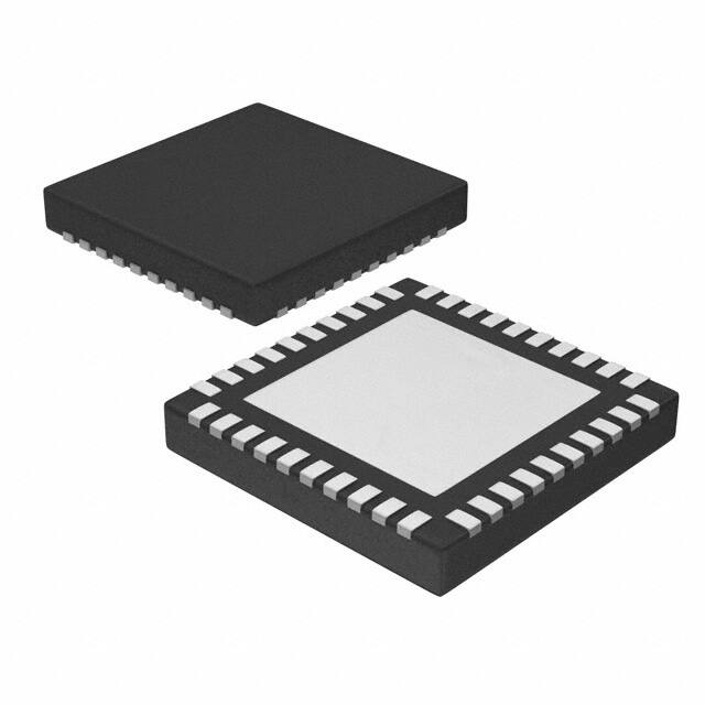


 工商网监
湘ICP备2023018690号
工商网监
湘ICP备2023018690号
