TPS40490
www.ti.com
SLVSCB4 – OCTOBER 2013
5-V to 60-V WIDE-INPUT SYNCHRONOUS PWM BUCK CONTROLLER
Check for Samples: TPS40490
FEATURES
1
•
•
•
•
•
•
•
Wide-Input Voltage Range from 5 V to 60 V
600-mV Reference Voltage With ±1% Accuracy
and External Modulation Capabilities
Programmable UVLO and Hysteresis
Voltage Mode Control With Feed Forward and
High Gain Bandwidth Error Amplifier
100-kHz to 5.4-MHz Programmable Frequency
Smart Low and High Side Driver
– Factory Selectable Gate Drive Voltage VDR
With External Drive Capability and UVLO
Protection
– Matched Low and High Side Propagation
Delay
– Programmable Fixed Delay Dead-time
Low-Side FET Sensing Overcurrent Protection
and High-Side FET Sensing Short-Circuit
Protection
•
•
•
•
•
•
Programmable Closed Loop Soft-Start
Supports Pre-Biased Outputs
Thermal Shutdown at 160°C With Hysteresis
Power Good Detector
Integrated Diode for Bootstrap Supply With
UVLO
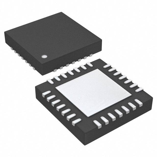
28-Pin 5-mm × 5-mm QFN (RHD) Package
APPLICATIONS
•
•
•
•
POL Modules
Wide Input Voltage, High-Power Density
DC/DC Converters for Industrial, Networking
and Telecomm Equipment
Notebook and Tablet Computers
Envelope Tracking Systems
TYPICAL APPLICATION (Non-Isolated 24V-12V Supply)
GND
VIN
GND
R20A
200K
J1
D1
J2
3.3V
VIN
R20B
10K
DT3
15
DT3
17
DT2
DT2
ILIM
PGOOD
20
19
RT
EN
16
R17
LDRVH
FB
LDRVL
SS
PGND
1
14
BSC123N08NS3G
Co7
0.1μF
OUT
1
L1
1μH
13
12
R13
2.2
11
R12
1.2
R27PM
0
R2
DNI
10
9
8
R10
2.2
R9
1.2
J3
2
Co1
Co2
Co3
Co4
Co5
Co6
47uF
47uF
47uF
47uF
47uF
47uF
SW
J4
GND
C27
2200pF
C4
DNI
R27A
20K
Q2
R27C
130
FB
BSC123N08NS3G
GND
R27B
1.05K
DT1
GND
SYNC
C1
Ci2
2.2μF
Q1
R14
0
OUT
1.0μF
Ci1
2.2μF
DT1
C28
68nF
2.2μF
7
28
C26b
30pF
SW
TPS40490
COMP
SYNC
27
18
R19
33K
R18
100K
FB
U1
V3V
6
C26
1nF
26
HDRVL
NUD
15K
R26
COMP
BOOT
VDR_EXT
NUC
25
C25
1.0uF
Ci4
2.2μF
SW
47nF
C14
HDRVH
5
24
Ci3
VIN
VDR
4
V3p3
GND
VDR_EXT
VIN
VREF
C24
4.7μF
23
3
22
GND
VIN
0.1μF
VOUT
C22
PAD
2
29
UVLO
21
C21
10000pF
C23
1.0uF
100K
V3p3
R21A
200K
R21B
10K
GND
C3
1nF
GND
GND
VDR_EXT
R1
1
2
C24A
0.1μF
C2
NC
220uF
20
OUT
D2
BAT43XV2
J6
JCOMP
1
Please be aware that an important notice concerning availability, standard warranty, and use in critical applications of
Texas Instruments semiconductor products and disclaimers thereto appears at the end of this data sheet.
PRODUCTION DATA information is current as of publication date.
Products conform to specifications per the terms of the Texas
Instruments standard warranty. Production processing does not
necessarily include testing of all parameters.
Copyright © 2013, Texas Instruments Incorporated
�TPS40490
SLVSCB4 – OCTOBER 2013
www.ti.com
DESCRIPTION
TPS40490 is a full-featured, synchronous PWM buck controller that operates with an input voltage from 5 V to
60 V and is optimized for high-power-density, high-reliability DC/DC converter applications using the latest
generation of MOSFET transistors.
TPS40490 can operate in multiple DC systems from 5 V to 60 V and provides accurate output voltage regulation
with ±1% ensured accuracy. The reference voltage can be modulated in applications that require a tracking
envelope supply.
The controller can be configured for voltage-mode control with input-voltage feed-forward compensation that
enables instant response to input voltage change. The switching frequency is programmable from 100 kHz to
5.4 MHz.
The controller has an enable pin that allows for system shutdown in a low-current mode and a delayed start-up
for sequencing purposes, and a soft-start pin that allows adjustable soft-start time by connecting a capacitor to
the pin.
TPS40490 has a complete set of system protection and monitoring features such as programmable UVLO,
programmable overcurrent protection (OCP) by sensing the low-side FET, selectable short-circuit protection
(SCP) by sensing the high-side FET and thermal shutdown. The current limit trip point is set with a resistor fitted
to the ILIM pin that enables the designer to adjust current limit by selecting an external resistor and optimize the
choice of inductor. Once an over-current lasting more than 4 cycles is sensed, the converter will shut down for
100 ms and then the start-up sequencing will begin again. If the overload has been removed, the converter will
ramp up and operate normally. If this is not the case, the converter will sense another over-current event and
shut down again, repeating the cycle (hiccup) until the failure is cleared.
The controller supports pre-biased output and provides an open-drain PGOOD signal. The PGOOD pin is pulled
low when the buck converter is pulled below 80% of the nominal output voltage. The PGOOD is pulled up
through an external resistor when all converter outputs are more than 90% of its nominal output voltage. The
default reset time is 100 ms. The polarity of the PGOOD is active high.
The device implements an internal thermal shutdown to protect itself if the junction temperature exceeds 160°C.
The thermal shutdown forces the device to stop operating when the junction temperature exceeds thermal trip
threshold. Once the die temperature decreases below 140°C, the device reinitiates the power up sequence.
Thermal shutdown hysteresis is 20°C.
ORDERING INFORMATION (1)
TA
–40°C to 125°C
(1)
(2)
2
DEVICE
VIN RANGE (V)
VDR (V)
TPS40490
MOSFET Low VIN
5 to 30
4.8
TPS40490
MOSFET High VIN
5 to 60
PACKAGE (2)
ORDERABLE PART NUMBER
TOP-SIDE MARKING
TPS40490MLRHDR/T
TPS40490ML
TPS40490MHRHDR/T
TPS40490MH
RHD-28
6.8
For the most current package and ordering information, see the Package Option Addendum at the end of this document, or see the TI
web site at www.ti.com.
Package drawings, thermal data, and symbolization are available at www.ti.com/packaging.
Submit Documentation Feedback
Copyright © 2013, Texas Instruments Incorporated
Product Folder Links: TPS40490
�TPS40490
www.ti.com
SLVSCB4 – OCTOBER 2013
These devices have limited built-in ESD protection. The leads should be shorted together or the device placed in conductive foam
during storage or handling to prevent electrostatic damage to the MOS gates.
BLOCK DIAGRAM
V IN
UVLO
V3P3
VIN
Selectable V
UVLO
V DR
VREF
V PULL
Digital Core
FB
VREF
VREF
Dead time
OR
VE X T
25K
PGOOD
controller
PGOOD
V DR _ EXT
OTFALT
OCFALT
Test pins
NUD
LDO_VDR
LDO3V
VO U T
NUC
Run
EN
V
Run
BOOT
DR
Run
HOST
HDRVH
OSCILLATOR
CLK
SYNC
+
HDRVIN
S
H
Q
R
SNSH
Lvlshift
DRVCTRL
LDRVOFF
HDRVOFF
tDEAD
HDRVIN
S
DRVCTRL
Q
R
Lvlshift
Control mode
OSC
V
HDRVL
SNSH
SW
SNSH
DR
V OUT
LDRV H
HDRVOFF
SNSL
Fault
Run
SS
Soft start
FB
LDRVL
LDRVOFF
- Soft Start
SNSL
SNSL
VOUT
VOUT
+ VREF
ILIMDET
ILIM
Overcurrent
controller
COMP
OC Fault
Run
CLK
EEPROM setting
Over Temperature
controller
DT1
1=Tie to 3v3
0 = open
DT2
DT3
FB
- Soft Start
+ VREF
OT Fault
VIN
+
-
ILIMDET
SW
+
-
tDEAD
Current limit detection
AGND
PGND
Submit Documentation Feedback
Copyright © 2013, Texas Instruments Incorporated
Product Folder Links: TPS40490
3
�TPS40490
SLVSCB4 – OCTOBER 2013
www.ti.com
4
UVLO
EN
RT
ILIM
PGOOD
DT2
DT3
PIN-OUT and TERMINAL FUNCTIONS
21
20
19
18
17
16
15
VIN
22
14
BOOT
VDR
23
13
HDRVH
VDR_EXT
24
12
HDRVL
V3V
25
11
SW
COMP
26
10
LDRVH
FB
27
9
LDRVL
SS
28
8
PGND
1
2
3
4
5
6
7
VOUT
AGND
VREF
NUC
NUD
SYNC
DT1
TPS40490
QFN RGE28
Submit Documentation Feedback
Copyright © 2013, Texas Instruments Incorporated
Product Folder Links: TPS40490
�TPS40490
www.ti.com
SLVSCB4 – OCTOBER 2013
PIN FUNCTIONS
NAME
I/O
PIN
DESCRIPTION
VOUT
I
1
Output voltage for the controller
AGND
GND
2
Analog signal ground. This pin must be electrically connected to power ground PGND externally.
VREF
O
3
Reference pin. A ceramic capacitor with a value between 1 nF and 100 nF must be connected between
this pin and the AGND pin and placed closely to this pin. This provides an RC filter with 25-kΩ resistor
inside the die.
NUC
-
4
Pin not used. Connect to ground during normal operation.
NUD
-
5
Pin not used. Connect to ground during normal operation.
SYNC
I
6
External synchronization pin.
DT1
I
7
Dead time set bit 1. Connect to 3V3 for 1, leave open for 0.
8
Power ground. This pin must externally connect to the AGND at a single point.
PGND
LDRVL
O
9
Low side gate driver turn-off output. Connect the gate of the low side transistor with a short, low
inductance path.
LDRVH
O
10
Low side gate driver turn-on output. Connect the gate of the low side transistor with a short, low
inductance path.
SW
O
11
This pin must connect to the switching node of the synchronous buck converter.
HDRVL
O
12
High side gate driver turn-off output. Connect the gate of the high side transistor with a short, low
inductance path.
HDRVH
O
13
High side gate driver turn-on output. Connect the gate of the high side transistor with a short, low
inductance path.
BOOT
O
14
Boot capacitor node for high-side FET gate driver supply. The boot capacitor is connected from this pin to
SW.
DT3
I
15
Dead time set bit 3. Connect to ground for 0, leave open for 1.
DT2
I
16
Dead time set bit 2. Connect to ground for 0, leave open for 1.
PGOOD
O
17
Power good indicator. This pin is an open-drain output pin and a 10-kΩ pull-up resistor is recommended
to be connected between this pin and V3V.
ILIM
I
18
A resistor from this pin to AGND sets the current limit. This pin provides source current used for over
current protection threshold setting.
RT
I
19
A resistor from this pin to AGND sets the oscillator frequency. Even if operating with an external
synchronization clock, it is required to have a resistor at this pin to set the free running switching
frequency.
EN
I
20
This pin must be high for the device to be enabled. If this pin is pulled low, the device is put in a lowpower consumption shutdown mode. Care must be taken to make sure the voltage at this pin does not
exceed 3.6 V.
UVLO
I
21
Undervoltage lockout. A resistor divider on this pin from VIN to AGND can be used to set the UVLO
threshold.
VIN
I
22
Input voltage for the controller which is also the input voltage for the DC/DC converter. A 1-µF to 10-µF
capacitor from this pin to AGND must be added and placed closed to VIN.
VDR
O
23
Regulated output for gate driver. A ceramic capacitor with a value between 1 µF and 10 µF must be
connected from this pin to PGND.
VDR_EXT
I
24
Optional External supply to gate driver. A ceramic capacitor with a value between 1 µF and 10 µF must
be connected from this pin to PGND. A supply of 5 V to 12 V can be connected to this input providing
drive voltage for better efficiency.
V3V
O
25
3.3-V regulated output. A ceramic by-pass capacitor of 1 µF must be connected between this pin and the
AGND pin and placed closely to this pin.
COMP
O
26
Output of the internal error amplifier. The feedback loop compensation network is connected from this pin
to the FB pin.
FB
I
27
Negative input to the error amplifier. The output voltage is fed back to this pin through a resistor divider
network.
SS
I
28
A capacitor must be connected at this pin to AGND. The capacitor value sets the soft-start time.
PAD
Power pad. Must be connected to PCB ground.
Submit Documentation Feedback
Copyright © 2013, Texas Instruments Incorporated
Product Folder Links: TPS40490
5
�TPS40490
SLVSCB4 – OCTOBER 2013
www.ti.com
ABSOLUTE MAXIMUM RATINGS
over operating free-air temperature range, (unless otherwise noted)
Input
(1) (2)
MIN
MAX
VIN, VOUT
–0.3
66
V
VDR_EXT
-0.3
13.2
V
RT, SS, FB, VREF, EN, PGOOD, V3V, ILIM, NUC, NUD, UVLO, SYNC, DT1,
DT2, DT3
–0.3
3.6
V
VDR, LDRVH, LDRVL, LDRV, COMP
–0.3
8.8
V
HDRVH, HDRVL
VSW
BOOT
V
BOOT-SW, HDRVH/HDRVL-SW, differential from BOOT or HDRVH/HDRVL
to SW
–0.3
VDR
V
–8
VIN
V
BOOT
–0.3
80V(VSW +
VDR)
V
GND-PGND, PGND-GND
–0.3
0.3
V
SW
Output
Ground
Power PAD to AGND (must be electrically connected externally to device)
Electrostatic discharge
(ESD)
Human body model (HBM)
UNIT
0
All pins excluding LDRVH and LDRVL
2000
LDRVH and LDRVL pins
1500
Charge device model (CDM)
V
500
Lead Temperature
260
°C
Operating junction temperature range, TJ
–40
150
°C
Storage temperature TSTG
–55
150
°C
(1)
(2)
Stresses beyond those listed under absolute maximum ratings may cause permanent damage to the device. These are stress ratings
only, and functional operatIon of the device at these or any other conditions beyond those indicted under recommended operating
conditions is not implied. Exposure it absolute maximum rated condtions for extended periods may affect device reliability.
Unless noted, all voltages are with respect to GND.
RECOMMENDED OPERATING CONDITIONS
over operating free-air temperature range (unless otherwise noted)
MIN
VIN
TA
(1)
6
TYP
MAX
UNIT
Input operating voltage, TPS40490MHRHDR
6
60
Input operating voltage, TPS40490MLRHDR
5 (1)
25
V
V
Ambient temperature
–40
125
°C
Operation with 5-V input is possible by connecting VIN pin to VDR. Consult with the factory.
Submit Documentation Feedback
Copyright © 2013, Texas Instruments Incorporated
Product Folder Links: TPS40490
�TPS40490
www.ti.com
SLVSCB4 – OCTOBER 2013
THERMAL INFORMATION
TPS40490
THERMAL METRIC (1)
θJA
Junction-to-ambient thermal resistance (1)
36.6
θJC(top)
Junction-to-case(top) thermal resistance (2)
26.2
θJB
Junction-to-board thermal resistance (3)
8.8
ψJT
Junction-to-top characterization parameter (4)
0.3
ψJB
Junction-to-board characterization parameter (5)
8.7
θJC(bottom)
(1)
(2)
(3)
(4)
(5)
(6)
Junction-to-case(bottom) thermal resistance
UNITS
RHD 28 pins
(6)
°C/W
1.9
For more information about traditional and new thermal metrics, see the IC Package Thermal Metrics application report, SPRA953.
The junction-to-case (top) thermal resistance is obtained by simulating a cold plate test on the package top. No specific JEDECstandard test exists, but a close description can be found in the ANSI SEMI standard G30-88.
The junction-to-board thermal resistance is obtained by simulating in an environment with a ring cold plate fixture to control the PCB
temperature, as described in JESD51-8.
The junction-to-top characterization parameter, ψJT, estimates the junction temperature of a device in a real system and is extracted
from the simulation data for obtaining θJA, using a procedure described in JESD51-2a (sections 6 and 7).
The junction-to-board characterization parameter, ψJB, estimates the junction temperature of a device in a real system and is extracted
from the simulation data for obtaining θJA, using a procedure described in JESD51-2a (sections 6 and 7.
The junction-to-case (bottom) thermal resistance is obtained by simulating a cold plate test on the exposed (power) pad. No specific
JEDEC standard test exists, but a close description can be found in the ANSI SEMI standard G30-88.
ELECTRICAL CHARACTERISTICS
TJ = –40°C to 150°C, VIN = 48 V, unless otherwise noted.
PARAMETER
TEST CONDITIONS
MIN
TYP
MAX
UNITS
INPUT SUPPLY
VIN
Input Voltage range
IDDSDN
Shutdown
VEN < 100 mV
5
2
60
µA
V
IDDQ
Quiescent, drivers not switching
VEN > 2 V, fSW = 1 MHz
2
mA
ENABLE
VDIS
Enable pin voltage to disable the
device
VEN
Enable pin voltage to enable the
device
IEN
Enable pin source current
300
1200
50
mV
mV
150
300
nA
VDR AND 3.3-V REGULATORS
VDR_MOSFET
Driver voltage regulator output
voltage
VDR_MOSFET_UVLO
Driver voltage UVLO MOSFET
rising edge
VDR_ACCURACY
Drive voltage accuracy
VDR_EXT_UVLO
External drive UVLO
V3p3
Internal biasing supply
TPS40490MLRHD: VEN ≥ 2 V, 5.6 V < VIN ≤ 60 V
4.8
TPS40490MHRHD: VEN ≥ 2 V, 6.8 V < VIN ≤ 60 V
6.8
TPS40490MHRHD
6.25
TPS40490MLRHD
4.4
-4.5
V
V
4.5
%
TPS40490MHRHD
11
TPS40490MLRHD
5
V
V
ILOAD = 0 to 10 mA
3.2
V
FIXED AND PROGRAMMABLE UVLO
VUVLO
Programmable UVLO ON voltage
IUVLO
Hysteresis current out of UVLO pin
870
900
930
5
mV
µA
REFERENCE
VREF
Reference voltage (+ input of the
error amplifier)
TJ = 25°C, 6 V < VVIN < 60 V
594
600
606
–40°C ≤ TJ 125°C, 6 V < VVIN ≤ 60 V
588
600
612
–40°C ≤ TJ 125°C, 5 V < VVIN ≤ 60 V
576
600
624
mV
OSCILLATOR
fsw
Switching frequency range
Set by external resistor
TPS40490MHRHD:
VVIN = 48 V
100
5400
TPS40490MLRHD:
VVIN = 12 V
100
5400
kHz
Submit Documentation Feedback
Copyright © 2013, Texas Instruments Incorporated
Product Folder Links: TPS40490
7
�TPS40490
SLVSCB4 – OCTOBER 2013
www.ti.com
ELECTRICAL CHARACTERISTICS (continued)
TJ = –40°C to 150°C, VIN = 48 V, unless otherwise noted.
PARAMETER
fsw_acc
Switching frequency set accuracy
VVALLEY
TEST CONDITIONS
MIN
PWM gain (VIN/VRAMP )
MAX
–12.5
12.5
TPS40490MLRHD:
VIN = 12 V, Rset = 100 kΩ, fSW = 1.75 MHz
–12.5
12.5
UNITS
%
Valley voltage
KPWM
TYP
TPS40490MHRHD:
VIN = 48 V, Rset = 31.6 kΩ, fSW = 1.15 MHz
0.7
1
1.31
V
TPS40490MLRHD: 5 V < VVIN ≤ 25 V
7.5
V/V
TPS40490MHRHD: 5 V < VVIN ≤ 60 V
20
V/V
5 V < VIN < 60 V
70
ns
PWM AND DUTY CYCLE (PWM control)
toff(MIN)
Minimum off-time
ERROR AMPLIFIER
GBWP
Gain bandwidth product
5 V < VIN < 60 V
40
MHz
AOL
Open loop gain
VREF = 0.6 V
75
dB
IIB
Input bias current
IEAOP
Output source current
VVFB = 0 V, VREF = 0.6 V, output grounded
4.2
mA
IEAOM
Output sink current
VVFB = 1 V, VREF = 0.6 V, output connected to 3-V supply
2.5
mA
100
nA
PROGRAMMABLE SOFT-START
Soft-start source current at
VSS < 0.5 V
ISS
VSS = 0.5 V
8.5
10.5
12.5
µA
GATE DRIVERS
VG
Gate voltage
RHDHI
High-side driver pull-up resistance
RHDLO
High-side driver pull-down
resistance
RLDHI
Low-side driver pull-up resistance
RLDLO
Low-side driver pull-down resistance
tRC
tFC
High side
VDR-0.6
Low side
VDR
V
0.7
Ω
0.35
Ω
0.7
Ω
CL = 1 nF, VDR = 5 V
0.35
Ω
Drive rise time
5
ns
Drive fall time
5
ns
DEAD TIME CONTROLLER (DTC) AND PROPAGATION DELAY
tDT_H2L_EXT
tDT_L2H_EXT
Dead time range HDRV fall and
LDRV rise
HDRV rise and LDRV fall
DT3
DT2
DT1
T(ns)
0
0
1
7.5
0
1
1
18
1
0
1
32
1
1
1
45
DT3
DT2
DT1
T(ns)
0
0
1
5
0
1
1
18
1
0
1
32
1
1
1
44
ns
ns
tDT_H2L_INT
Dead time internal
HDRV fall and LDRV rise
(Internal value fixed 001)
Measured dead time will be the highest of
tDEAD_TIME_INT, tDEAD_TIME_EXT
7.5
ns
tDT_L2H_INT
Dead time internal
HDRV rise and LDRV fall
(Internal value fixed 001)
Measured dead time will be the highest of
tDEAD_TIME_INT, tDEAD_TIME_EXT
5
ns
tDEAD_TIME_ACC
Accuracy dead time setting
Percentage of set time 001 setting
tHPHL
high turn-off propagation delay
Falling gate voltage, 0 ns DTC time
25
ns
tHPLH
High turn-off propagation delay
Rising gate voltage, 0 ns DTC time
25
ns
tLPHL
Low turn-off propagation delay
Falling gate voltage, 0 ns DTC time
25
ns
tLPLH
Low turn-off propagation delay
Rising gate voltage, 0 ns DTC time
25
Delay matching
HS gate off to LS gate ON, 0 ns DTC time
8
Submit Documentation Feedback
–10%
–4
10%
0
ns
4
ns
Copyright © 2013, Texas Instruments Incorporated
Product Folder Links: TPS40490
�TPS40490
www.ti.com
SLVSCB4 – OCTOBER 2013
ELECTRICAL CHARACTERISTICS (continued)
TJ = –40°C to 150°C, VIN = 48 V, unless otherwise noted.
PARAMETER
TEST CONDITIONS
MIN
TYP
MAX
UNITS
OVERCURRENT PROTECTION (LOW-SIDE MOSFET SENSING)
ILIM_PIN
ILIM pin voltage
5 V < VIN < 60 V, TJ = 25°C
ILIM_Tc
Temperature coefficient of ILIM
current
5 V < VIN < 60 V
1.23
V
25
ppm
°C
THERMAL SHUTDOWN
TTRIP
Thermal S/D trip point
Rising temperature
160
THYST
Thermal S/D hysteresis
Device re-starts
140
°C
TTRIP_DEGLITCH
Thermal S/D deglitch
110
µS
Output falling
80
%
Output rising (PGOOD asserted)
90
%
us
POWER GOOD
VUVBUCKX
Under voltage threshold
tBUCKUV_deglitch
Deglitch time
Both edges
110
tVINUV_deglitch
Deglitch time
Both edges
110
us
tON_HICCUP
Hiccup mode ON time
VUVBUCKX asserted
10
ms
tOFF_HICCUP
Hiccup mode OFF time
Converter disabled. Once tOFF_HICCUP elapses, converter
will go through start-up again
100
ms
VOVBUCKX
Threshold voltage for buck OVP %
of Vset
Output rising (high side FET will be forced off)
114
%
Submit Documentation Feedback
Copyright © 2013, Texas Instruments Incorporated
Product Folder Links: TPS40490
9
�TPS40490
SLVSCB4 – OCTOBER 2013
www.ti.com
TYPICAL CHARACTERISTICS
10
Figure 1. Vref and Vout start-Up Vin=48V Vo=12V
Figure 2. SS Vin=24V, Cref=1nF, CVdr=1µF,
Cv3V=1µF, css=68nF, Io=5.5A
Figure 3. Start-up 15Vin Vo=5.8V, 6A, 5MHz
Figure 4. Start-up 22Vin Vo=5.8V, 6A, 5MHz
Figure 5. Soft-Start with Vout connected to Vdr_ext with
diode +20 Ω 200µF Yellow=Vout, Purple=Vdr_ext Blue=Vdr,
Green=IC current
Figure 6. Detailed start-up operation, 24Vin, Vo=12V, 6A
Ch1 (yellow): FB pin (negative input to the error amplifier),
Ch2 (blue): Vout,
Submit Documentation Feedback
Copyright © 2013, Texas Instruments Incorporated
Product Folder Links: TPS40490
�TPS40490
www.ti.com
SLVSCB4 – OCTOBER 2013
TYPICAL CHARACTERISTICS (continued)
Figure 7. Switching node signals 24Vin, Vo=12V, 0A
Ch1 (yellow): Vgate_high (measured on FET),
Ch2 (blue): switching node, Ch3 (purple): Vgate_low
(measured on FET), Ch4 (green): Load current
Figure 8. Switching node signals 24Vin, Vo=12V, 6A
Ch1 (yellow): Vdrive_external), Ch2 (blue): switching node
Ch3 (purple): Vout, Ch4 (green): Vin
Figure 9. Detailed fall time plots, 24Vin, Vo=12V 6A out
Ch1 (yellow): Vgate_high (measured on FET),
Ch2 (blue): switching node Ch3 (purple): Vgate_low
(measured on FET), Ch4 (green): Load current.
Figure 10. Detailed rise time plots, 24Vin, Vo=12V 6A out
Ch1 (yellow): Vgate_high (measured on FET),
Ch2 (blue): switching node Ch3 (purple): Vgate_low
(measured on FET), Ch4 (green): Load current.
Figure 11. Sw node 1.8MHz
Figure 12. Sw node 4.7MHz operation 22Vin Vo=4.7V, Io=6A
Ch1 (yellow): Switching node, Ch2 (blue): Vout
Ch3 (purple): COMP, Ch4 (green): Load current.
Submit Documentation Feedback
Copyright © 2013, Texas Instruments Incorporated
Product Folder Links: TPS40490
11
�TPS40490
SLVSCB4 – OCTOBER 2013
www.ti.com
TYPICAL CHARACTERISTICS (continued)
12
Figure 13. Gate drive and switching node fsw=1.5MHz,
no load
Figure 14. Gate drive and switching node
fsw=1.5MHz, Io=7A
Figure 15. High Gate drive and switching node, fsw= 5MHz
Figure 16. Low Gate drive and switching node, fsw=5MHz
Figure 17. Current limit operation Rds_on= 13mΩ,
Rlim=128kΩ Ch1 (yellow): output current,
Ch2 (blue): switching node Ch3 (purple): output voltage,
Ch4 (green): input voltage
Figure 18. Expanded Current limit operation
Rds_on= 13mΩ, Rlim=128kΩ Ch1 (yellow): output current,
Ch2 (blue): switching node Ch3 (purple): output voltage,
Ch4 (green): input voltage.
Submit Documentation Feedback
Copyright © 2013, Texas Instruments Incorporated
Product Folder Links: TPS40490
�TPS40490
www.ti.com
SLVSCB4 – OCTOBER 2013
TYPICAL CHARACTERISTICS (continued)
Figure 19. Sync at 2MHz, Vin=24V, Vo=5V From top to
bottom COMP, Iout, Vsw, vsync
Figure 20. Sync at 3MHz, Vin=24V, Vo=5V COMP, Iout, Vsw,
vsync
Figure 21. Dead time setting to 111 (42ns typ)
Ch1 (yellow): Switching node, Ch2 (blue): Vg high side
Ch3 (purple): Vg low side
Figure 22. Dead time setting to 011 (18ns typ)
Ch1 (yellow): Switching node, Ch2 (blue): Vg high side
Ch3 (purple): Vg low side
Figure 23. System efficiency improvement with different
dead times Vin=12 Vo= 3.3V 1.25MHz
Figure 24. System efficiency variation with
gate drive voltage Vin=48V, Vo=30V,
f=1.25MHz 80V MOSFETs (for information only)
Submit Documentation Feedback
Copyright © 2013, Texas Instruments Incorporated
Product Folder Links: TPS40490
13
�TPS40490
SLVSCB4 – OCTOBER 2013
www.ti.com
TYPICAL CHARACTERISTICS (continued)
14
Figure 25. Efficiency at Vo=30V
Figure 26. Thermal plot (forced air) Vin=36V Vo=30V,
Io=6A fsw=1MHz, TA=25°C
Figure 27. 1.1MHz Vo=12V efficiency
with MOSFET BSC123N08NS3G
Figure 28. 2.5MHz Vo=12V efficiency
with MOSFET BSC123N08NS3G
Figure 29. 200kHz Modulated output
10-30V, 3Ω load, fsw=1.5MHz
Figure 30. 200kHz modulated output
5-15V, 1.5Ω load, fsw= 1.5MHz
Submit Documentation Feedback
Copyright © 2013, Texas Instruments Incorporated
Product Folder Links: TPS40490
�TPS40490
www.ti.com
SLVSCB4 – OCTOBER 2013
TYPICAL CHARACTERISTICS (continued)
Figure 31. Ripple 18Vin Vo=3.3V, 10A 2.25MHz
Figure 32. Ripple 8Vin Vo=6V, 6A 5MHz
Figure 33. Ripple at 1MHz Vin=48V, Vo=30V,
Io=10A Lo=1µH, Co=12µF ceramic
Figure 34. Ripple at 1MHz Vin=48V,
Vo=30V, Io=10A Lo=1µH,
Co=12µF ceramic +470µF electrolytic
Figure 35. Transient response,
10A step down load1MHz Vin=48V, Vo=30V,
Io=10A Lo=1µH, Co=12µF ceramic
Figure 36. Transient response,
10A step down load1MHz Vin=48V, Vo=30V,
Io=10A Lo=1µH, Co=12µF ceramic
Submit Documentation Feedback
Copyright © 2013, Texas Instruments Incorporated
Product Folder Links: TPS40490
15
�TPS40490
SLVSCB4 – OCTOBER 2013
www.ti.com
TYPICAL CHARACTERISTICS (continued)
16
Figure 37. Transient step response
Vin=15V, Vo=3.3V 2.2MHz 1-8A
Figure 38. Transient step response
Vin=24V, Vo=5V 5MHz 1-10A Fc=140kHz
Figure 39. Transient step response
Vin=24V, Vo=5V 5MHz 1-7A,Fc=140kHz
Ch1 (yellow):Switching node, Ch2 (blue):Vo,
Ch3 (purple): COMP, CH4(green): Io
Figure 40. Transient step response
Vin=24V, Vo=5V 5MHz 1-7A,Fc=600kHz
Ch1 (yellow): Switching node, Ch2 (blue):COMP,
Ch3 (purple): Vo, CH4(green): Io
Figure 41. Steady state operation
Vin=12, Vo=3.3V 5MHz No load Ch1 (yellow):
Switching node, Ch3 (purple): Vout, CH4(green): Io
Figure 42. Steady state operation
Vin=12, Vo=3.3V 5MHz 5A Ch1 (yellow):
Switching node, Ch3 (purple): Vout, CH4(green): Io
Submit Documentation Feedback
Copyright © 2013, Texas Instruments Incorporated
Product Folder Links: TPS40490
�TPS40490
www.ti.com
SLVSCB4 – OCTOBER 2013
TYPICAL CHARACTERISTICS (continued)
Figure 43. 0-5A step load Vin=12 Vo=3.3V fsw=5MHz,
Ch3 (purple): Vout, CH4(green): Io
Figure 44. 5-0A load dump Vin=12 Vo=3.3V fsw=5MHz,
Ch3 (purple): Vout, CH4(green): Io
Submit Documentation Feedback
Copyright © 2013, Texas Instruments Incorporated
Product Folder Links: TPS40490
17
�TPS40490
SLVSCB4 – OCTOBER 2013
www.ti.com
TPS40490 STATE MACHINE
nPUC=0
(nPUC=(EN=1) && (V3V>2.6V)
Reset State
nPUC=1
Read EEPROM
nPUC=1
Wait for 1msec
FaultINT=1
nPUC=1
Check Internal
Biases
FaultINT=0
Pre enable state
BUCK_EN_PRE=1
BUCK_EN=0
FaultINT=0
Wait for 100usec
Wait for
100msec
FaultINT=0
FaultINT=1 || FaultEXT=1
Enable state
BUCK_EN_PRE=1
BUCK_EN=1
FaultINT=(VDRV_UVdeg=1) || (VINUVdeg=1) || (OTSdeg=1)
FaultEXT=(VBUCK_UVdeg=1) || (ILIM_LATCH=1)
18
Submit Documentation Feedback
Copyright © 2013, Texas Instruments Incorporated
Product Folder Links: TPS40490
�TPS40490
www.ti.com
SLVSCB4 – OCTOBER 2013
APPLICATION INFORMATION
TYPICAL APPLICATION CIRCUIT
The following page contains the TPS40490 application circuit.
GND
VIN
GND
R20A
200K
J1
D1
J2
3.3V
VIN
R20B
10K
DT3
DT2
15
DT3
DT2
ILIM
PGOOD
18
20
19
RT
EN
FB
LDRVL
SS
PGND
1
14
R14
0
BSC123N08NS3G
12
R13
2.2
0.1μF
11
R12
1.2
R27PM
0
R2
DNI
10
R10
2.2
R9
1.2
9
8
J3
2
Co1
Co2
Co3
Co4
Co5
Co6
47uF
47uF
47uF
47uF
47uF
47uF
SW
J4
GND
C27
2200pF
C4
DNI
R27A
20K
Q2
R27C
130
FB
BSC123N08NS3G
R27B
1.05K
DT1
GND
Co7
OUT
1
L1
1μH
13
GND
SYNC
1.0μF
Ci2
2.2μF
Q1
OUT
C1
Ci1
2.2μF
DT1
C28
68nF
2.2μF
7
28
C26b
30pF
16
R17
27
LDRVH
SYNC
FB
SW
TPS40490
COMP
NUD
C26
1nF
U1
V3V
6
15K
R26
26
17
R19
33K
R18
100K
COMP
HDRVL
NUC
25
C25
1.0uF
47nF
C14
BOOT
VDR_EXT
5
24
Ci4
2.2μF
VIN
HDRVH
4
V3p3
GND
VDR_EXT
Ci3
SW
VDR
VREF
C24
4.7μF
23
VIN
3
0.1μF
PAD
GND
22
VOUT
VIN
2
29
C22
UVLO
21
C21
10000pF
C23
1.0uF
100K
V3p3
R21A
200K
R21B
10K
GND
C3
1nF
GND
GND
VDR_EXT
R1
1
2
C24A
0.1μF
C2
NC
220uF
20
OUT
D2
BAT43XV2
J6
JCOMP
ENABLE CIRCUIT
VIN
R EN_H
VIN
EN
–
R EN_L
V DIS
(300 mV)
Disable
+
AGND
The internal LDOs are enabled if the enable pin is higher than VEN. When VEN is less than 300 mV, the device is
fully disabled and the current consumption is less than 2 µA. The internal LDOs are actively discharged. The
enable pin must not be allowed to float. If the function is not needed for the design, EN should be pulled up to
VIN by a high value resistor ensuring that the current into the enable pin does not exceed 10 μA. If it is not
possible to meet this clamp current requirement, a resistor divider from VIN to GND be used to connect to EN.
The resistor divider should be such that the enable pin should be higher than VEN and lower than 3.3 V. A
capacitor can be used to provide additional start-up delay. To avoid potential erroneous behavior of the enable
function, the enable signal applied must have a minimum slew rate of 20 V/s.
Submit Documentation Feedback
Copyright © 2013, Texas Instruments Incorporated
Product Folder Links: TPS40490
19
�TPS40490
SLVSCB4 – OCTOBER 2013
www.ti.com
UVLO CIRCUIT
I UVLO
V IN
R UV_H
VIN
UVLO
V IN _ OK
+
V UVLO
C UVLO
-
R UV_L
A GND
TPS40490 has both fixed and programmable input UVLO. For the device to turn-on, the enable pin must be
greater than VEN and the UVLO voltage higher than 900 mV (typ). Once the input voltage reaches UVLO, a small
5-µA hysteresis current source is switched on.
To calculate the UVLO divider use the following formula:
RUV_H = (VON – VOFF)/IUVLO
RUV_L = RUV_H × VUVLO/(VON–VUVLO)
Where:
VON = Desired turn-on voltage
VOFF = Desired turn-off voltage
IUVLO = Hysteresis current (5 µA)
VUVLO = UVLO threshold voltage
20
Submit Documentation Feedback
Copyright © 2013, Texas Instruments Incorporated
Product Folder Links: TPS40490
�TPS40490
www.ti.com
SLVSCB4 – OCTOBER 2013
SOFT-START
I UVLO
SS
Soft-start
chrge/
discharge
control
V3P3
C SS
V3P3
VREF
+
+
A GND
FB
COMP
As the SS pin voltage approaches 0.65 V, the positive input to the error amplifier begins to rise and the output of
the error amplifier (COMP pin) starts rising. The rate of rise of the COMP voltage is mainly limited by the
feedback loop compensation network. Switching begins once VCOMP reaches the valley of the PWM ramp. The
output is regulated to the error amplifier input through the FB pin in the feedback loop. When the FB pin reaches
the 600-mV reference voltage, the feedback node is regulated to the reference voltage, VREF. The SS pin
continues to rise and is clamped to VDD.
The formula to calculate the soft-start capacitor is
CSS = tss/0.09
CSS = Soft-Start capacitance (nF)
tSS = Soft-Start time (ms)
Submit Documentation Feedback
Copyright © 2013, Texas Instruments Incorporated
Product Folder Links: TPS40490
21
�TPS40490
SLVSCB4 – OCTOBER 2013
www.ti.com
OSCILLATOR AND VIN FEED-FORWARD
The resistor at the RT pin sets the current. The proportional current charges an internal 20-pF oscillator
capacitor. The ramp voltage on this capacitor is compared with the RT pin voltage, VRT. Once the ramp voltage
reaches VRT, the oscillator capacitor is discharged. The ramp that is generated by the oscillator (which is
proportional to the input voltage) acts as a voltage feed-forward ramp to be used in the PWM comparator.
The frequency of operation of the device can be set according to the following formulae:
TPS40490MHRHDR: RT (kΩ) = 37.5/fSW (MHz)
TPS40490MLRHDR: RT (kΩ) = 176.5/fSW (MHz)
(1)
(2)
It is important to keep in mind the following two requirements when using TPS40490MLRHDR with operating
voltage in the 24 V to 30 V range:
1. There is a restriction on the minimum set frequency for voltages as the following graph shows.
2. There is a shift in the switching frequency as the following graph shows for a setting of 1.7 MHz at 12 V.
External Clock
When synchronization is applied, the PWM oscillator frequency must be lower (70-80%) than the sync pulse
frequency. The SYNC pin will be ignored during start-up and when PGOOD is not asserted. The SYNC pin must
be tied to GND when the feature is not used.
22
Submit Documentation Feedback
Copyright © 2013, Texas Instruments Incorporated
Product Folder Links: TPS40490
�TPS40490
www.ti.com
SLVSCB4 – OCTOBER 2013
+
Iref
–
ILSref2=1X-2X of Iref
1.23V
ILSref1=1X-2X of Iref
Current Limit Operation
IHSref=Kx of Iref
Rext
There are two different current limit mechanisms in TPS40490, high-side (HS) and low-side (LS). HS and LS
values are adjustable through an external resistor Rext. A reference current of 1.23 V/RESext is generated first.
This current is going to be mirrored for HS and LS. The current limit circuit does not have temperature
adjustment.
-
10k
ILSref2=1X-2X of Iref
5k
-
VSW
ILSref1=1X-2X of Iref
LS_ON
ISW
Low Side Current Limit
LS
FET
LSdet
+
5k
+
The formula to calculate the low side current limit is,
10k 1.23
ILS -lim = 1.75
RLS _ ON Rext
(3)
where RLS_ON is LS switch on resistance.
Submit Documentation Feedback
Copyright © 2013, Texas Instruments Incorporated
Product Folder Links: TPS40490
23
�TPS40490
SLVSCB4 – OCTOBER 2013
www.ti.com
High Side Current Limit
VBOOT
VIN
VIN
10k
HS
FET
HSdet
+
-
IHSref k of Iref
VSW
IL=Inductor current
HS_ON
inverted
The formula to calculate the high side current limit is,
10k 1.23
IHS -lim = K
RHS _ ON Rext
(4)
where RHS_ON is high-side switch on resistance and K is the current limit multiple (5).
Shut-Down Counter
HS and LS current detect signals will go to the input of a 4x up/down counter. If there is a current limit detect, the
counter will count up. In the next cycle, if there is another current limit detect, the counter counts up again, but if
there is no current limit detected, the counter counts down and when at zero count, it stays there.
If there are consecutive current faults, the counter overflows, and ILIMlatched will be set to 1. This will inform the
digital core of a current limit fault, the driver and oscillator will be disabled and a new soft-start will be initiated
after 100 ms.
24
Submit Documentation Feedback
Copyright © 2013, Texas Instruments Incorporated
Product Folder Links: TPS40490
�TPS40490
www.ti.com
SLVSCB4 – OCTOBER 2013
VDR and VDR_EXT
VIN
EN_ Vext
EN pin
Vtarget
EN
Vtarget
+
-
+
EN_Vext
-
EN pin
80 V
device
-
EN
EN_ Vext
VIN
+
-
12 V
device
VDRVuvlo
- .
Max
13.2V
+
VDRV
C DRVext
VDRVext
C DRV
The driver voltage is set to 4.8 V or 6.8 V according to the device version. If an external drive voltage is applied,
the internal driver voltage will be regulated internally to pre-set factory voltage. The decoupling capacitor should
be fitted very close to the VDR and VDR_EXT.
Submit Documentation Feedback
Copyright © 2013, Texas Instruments Incorporated
Product Folder Links: TPS40490
25
�TPS40490
SLVSCB4 – OCTOBER 2013
www.ti.com
Driver Circuits
The high side driver is designed as a floating driver that can be connected either as a high side in a system
operating up to 60 V or connected to ground with a programmable dead time controller.
VIN
Boot
VDRV
V3V
HS_ON
Lvlshift
V3V
Driver
Deadtime
control
IN
SW
VDRV
LS_ON
Lvlshift
V3V
Driver
PGND
Fixed Dead Time Control
DT1 DT2 DT3
VIN
IN
S
DRV_CTRL
Q
Lvlshift
HDRVIN
External
setting
Driver
R
S
DRV_EN
Q
DRV_CTRL
Lvlshift
SW
Driver
R
GND
The device is provided with a programmed dead time of 6 ns and can be increased by setting the DT1 to DT3
pins.
26
Submit Documentation Feedback
Copyright © 2013, Texas Instruments Incorporated
Product Folder Links: TPS40490
�TPS40490
www.ti.com
SLVSCB4 – OCTOBER 2013
Feed-Forward PWM Mode
The configuration for PWM operation is shown in the following figure.
OSC
V3P3
ΔVOSC
C CMP
VOUT
2
+
COMP
C FB _H
R FB _H
C CMP 1
R FB _H1
PWM
Comparator
R CMP 1
V3P3
FB
R FB _L
+
VREF
A type 3 compensation circuit is recommended for this type of operation. It's transfer function is:
GAINT3 =
RFB _ H1 + RFB _ H
RFB _ H1 * RFB _ H * CCMP2
*
ö
æ
ö æ
1
1
ç
÷
s
s
+
*
+
ç
÷
RCMP1 * CCMP1 ø ç
RFB _ H1 + RFB _ H * CFB _ H ÷
è
è
ø
(
)
ö
æ
ö æ
CCMP1 + CCMP
1
÷
s * çs +
÷ *çs +
ç
÷
R
*
C
*
C
R
*
C
CMP1
CMP1
CMP1
è
ø è
FB _ H1
FB _ H ø
(
)
Submit Documentation Feedback
Copyright © 2013, Texas Instruments Incorporated
Product Folder Links: TPS40490
(5)
27
�TPS40490
SLVSCB4 – OCTOBER 2013
www.ti.com
A typical transfer function plot is:
1/(2(RFB_H+RFB_HI)CFB_H)
GAIN (dB)
1/(2RCMP1(CCMP1CCMP2 /(CCMP1+CCMP2)))
1/(2RFB_HICFB_H)
20*log(RCOMP/RFB_H
Frequency (Hz)
PHASE (°)
1/(2RCMP1CCMP1)
180° BOOST
Frequency (Hz)
The system gain is:
SYSGAIN =
RFB _ H1 + RFB _ H
RFB _ H1 * RFB _ H * CCMP2
*
ö
æ
ö æ
1
1
÷
çs +
÷ *çs +
ç
RCMP1 * CCMP1 ø
RFB _ H1 + RFB _ H * CFB _ H ÷
è
è
ø
(
)
ö
æ
ö æ
CCMP1 + CCMP
1
÷
s * çs +
÷ *çs +
ç
RCMP1 * CCMP1 * CCMP1 ø
RFB _ H1 * CFB _ H ÷
è
è
ø
(
*
1 + s * ESR * COUT
VIN
*
DVOSC 1 + s * (ESR + DCR )* COUT + s2 * LOUT * COUT
)
(6)
28
Submit Documentation Feedback
Copyright © 2013, Texas Instruments Incorporated
Product Folder Links: TPS40490
�TPS40490
www.ti.com
SLVSCB4 – OCTOBER 2013
To calculate the external compensation components follow the following steps:
ACTION
Define switching frequency (fSW), output
filter parameters, L and C, output filter
resonant frequency and output capacitor
ESR zero frequency.
FORMULA
fLC =
fESR =
COMMENT
1
2p IOUT · COUT
(7)
1
2p•ESR•COUT
(8)
Pick RFB_H
Calculate RFB_L
Suggested to use a value lower than 10 kΩ.
RFB_H
VOUT
-1
VREF
RFB_L =
th
Set the value according to required output
voltage.
(9)
th
Determine loop desired bandwidth
BW = 1/5 to 1/10 of fSW
Calculate RCMP1
RCMP1 =
Calculate CCMP1
Calculate CCMP2
Calculate RFB_H1
Calculate CFB_H
BW
•RFB_H
fLC · KPWM
Used to achieve the desired bandwidth
(11)
1
CCMP1 =
p · fLC · KPWM
(12)
1
2p · RCMP1 · CPCMP1 · fESR -1 (13)
CCMP2 =
RFB_H1 =
CFB_H =
(10) Suggested range
RFB_H
fSW
-1
2•fLC
1
p · RFB_H1 · fSW
Places a zero at ~50% of the output filter double
pole frequency
Places first pole at the output capacitor ESR
frequency
Places second pole at half the switching
frequency
(14)
(15)
Places second zero at the output filter double
pole
Submit Documentation Feedback
Copyright © 2013, Texas Instruments Incorporated
Product Folder Links: TPS40490
29
�TPS40490
SLVSCB4 – OCTOBER 2013
www.ti.com
Minimum Controllable On-Time
When operating in voltage mode control TPS40490 does not have any restrictions associated with a minimum
on-time (as it occurs with current mode control circuits due to the blanking of the leading edge inductor current).
Figure 45. Simulation Plot Showing Error (COMP)
VoltageRequired to Provide a Narrow Switching
Pulse
Figure 46. Detail of Error (COMP) Voltage and PWM
Ramp
As the simulation plots show the difference between the start of the PWM ramp and the error voltage is around
100 mV or less, therefore generating specific challenges on applications requiring a narrow pulse operation:
1. Attention must be paid to layout to avoid noise imposed on the COMP and internal ramp to avoid spurious
trips of the PWM comparator.
2. It is important to pick the right transistor for the application. If rise and fall times are comparable to the
minimum on time, it is possible to have a jitter effect on the switching node.
SW node
t on(MIN)
tr
Controllable
on-time
tf
The combined rise and fall time (tr and tf shown above) should meet the following:
tr + tf < 0.1 × ton(MIN)
30
Submit Documentation Feedback
Copyright © 2013, Texas Instruments Incorporated
Product Folder Links: TPS40490
�PACKAGE OPTION ADDENDUM
www.ti.com
17-Nov-2013
PACKAGING INFORMATION
Orderable Device
Status
(1)
Package Type Package Pins Package
Drawing
Qty
Eco Plan
Lead/Ball Finish
MSL Peak Temp
(2)
(6)
(3)
Op Temp (°C)
Device Marking
(4/5)
TPS40490MHRHDR
ACTIVE
VQFN
RHD
28
3000
Green (RoHS
& no Sb/Br)
CU NIPDAU
Level-3-260C-168 HR
-40 to 150
TPS
40490MH
TPS40490MHRHDT
ACTIVE
VQFN
RHD
28
250
Green (RoHS
& no Sb/Br)
CU NIPDAU
Level-3-260C-168 HR
-40 to 150
TPS
40490MH
TPS40490MLRHDR
PREVIEW
VQFN
RHD
28
3000
Green (RoHS
& no Sb/Br)
CU NIPDAU
Level-3-260C-168 HR
-40 to 150
TPS
40490ML
TPS40490MLRHDT
PREVIEW
VQFN
RHD
28
250
Green (RoHS
& no Sb/Br)
CU NIPDAU
Level-3-260C-168 HR
-40 to 150
TPS
40490ML
(1)
The marketing status values are defined as follows:
ACTIVE: Product device recommended for new designs.
LIFEBUY: TI has announced that the device will be discontinued, and a lifetime-buy period is in effect.
NRND: Not recommended for new designs. Device is in production to support existing customers, but TI does not recommend using this part in a new design.
PREVIEW: Device has been announced but is not in production. Samples may or may not be available.
OBSOLETE: TI has discontinued the production of the device.
(2)
Eco Plan - The planned eco-friendly classification: Pb-Free (RoHS), Pb-Free (RoHS Exempt), or Green (RoHS & no Sb/Br) - please check http://www.ti.com/productcontent for the latest availability
information and additional product content details.
TBD: The Pb-Free/Green conversion plan has not been defined.
Pb-Free (RoHS): TI's terms "Lead-Free" or "Pb-Free" mean semiconductor products that are compatible with the current RoHS requirements for all 6 substances, including the requirement that
lead not exceed 0.1% by weight in homogeneous materials. Where designed to be soldered at high temperatures, TI Pb-Free products are suitable for use in specified lead-free processes.
Pb-Free (RoHS Exempt): This component has a RoHS exemption for either 1) lead-based flip-chip solder bumps used between the die and package, or 2) lead-based die adhesive used between
the die and leadframe. The component is otherwise considered Pb-Free (RoHS compatible) as defined above.
Green (RoHS & no Sb/Br): TI defines "Green" to mean Pb-Free (RoHS compatible), and free of Bromine (Br) and Antimony (Sb) based flame retardants (Br or Sb do not exceed 0.1% by weight
in homogeneous material)
(3)
MSL, Peak Temp. - The Moisture Sensitivity Level rating according to the JEDEC industry standard classifications, and peak solder temperature.
(4)
There may be additional marking, which relates to the logo, the lot trace code information, or the environmental category on the device.
(5)
Multiple Device Markings will be inside parentheses. Only one Device Marking contained in parentheses and separated by a "~" will appear on a device. If a line is indented then it is a continuation
of the previous line and the two combined represent the entire Device Marking for that device.
(6)
Lead/Ball Finish - Orderable Devices may have multiple material finish options. Finish options are separated by a vertical ruled line. Lead/Ball Finish values may wrap to two lines if the finish
value exceeds the maximum column width.
Addendum-Page 1
Samples
�PACKAGE OPTION ADDENDUM
www.ti.com
17-Nov-2013
Important Information and Disclaimer:The information provided on this page represents TI's knowledge and belief as of the date that it is provided. TI bases its knowledge and belief on information
provided by third parties, and makes no representation or warranty as to the accuracy of such information. Efforts are underway to better integrate information from third parties. TI has taken and
continues to take reasonable steps to provide representative and accurate information but may not have conducted destructive testing or chemical analysis on incoming materials and chemicals.
TI and TI suppliers consider certain information to be proprietary, and thus CAS numbers and other limited information may not be available for release.
In no event shall TI's liability arising out of such information exceed the total purchase price of the TI part(s) at issue in this document sold by TI to Customer on an annual basis.
Addendum-Page 2
�PACKAGE MATERIALS INFORMATION
www.ti.com
18-Nov-2013
TAPE AND REEL INFORMATION
*All dimensions are nominal
Device
Package Package Pins
Type Drawing
SPQ
Reel
Reel
A0
Diameter Width (mm)
(mm) W1 (mm)
B0
(mm)
K0
(mm)
P1
(mm)
W
Pin1
(mm) Quadrant
TPS40490MHRHDR
VQFN
RHD
28
3000
330.0
12.4
5.3
5.3
1.5
8.0
12.0
Q2
TPS40490MHRHDT
VQFN
RHD
28
250
180.0
12.4
5.3
5.3
1.5
8.0
12.0
Q2
Pack Materials-Page 1
�PACKAGE MATERIALS INFORMATION
www.ti.com
18-Nov-2013
*All dimensions are nominal
Device
Package Type
Package Drawing
Pins
SPQ
Length (mm)
Width (mm)
Height (mm)
TPS40490MHRHDR
VQFN
RHD
28
3000
367.0
367.0
35.0
TPS40490MHRHDT
VQFN
RHD
28
250
210.0
185.0
35.0
Pack Materials-Page 2
����IMPORTANT NOTICE
Texas Instruments Incorporated and its subsidiaries (TI) reserve the right to make corrections, enhancements, improvements and other
changes to its semiconductor products and services per JESD46, latest issue, and to discontinue any product or service per JESD48, latest
issue. Buyers should obtain the latest relevant information before placing orders and should verify that such information is current and
complete. All semiconductor products (also referred to herein as “components”) are sold subject to TI’s terms and conditions of sale
supplied at the time of order acknowledgment.
TI warrants performance of its components to the specifications applicable at the time of sale, in accordance with the warranty in TI’s terms
and conditions of sale of semiconductor products. Testing and other quality control techniques are used to the extent TI deems necessary
to support this warranty. Except where mandated by applicable law, testing of all parameters of each component is not necessarily
performed.
TI assumes no liability for applications assistance or the design of Buyers’ products. Buyers are responsible for their products and
applications using TI components. To minimize the risks associated with Buyers’ products and applications, Buyers should provide
adequate design and operating safeguards.
TI does not warrant or represent that any license, either express or implied, is granted under any patent right, copyright, mask work right, or
other intellectual property right relating to any combination, machine, or process in which TI components or services are used. Information
published by TI regarding third-party products or services does not constitute a license to use such products or services or a warranty or
endorsement thereof. Use of such information may require a license from a third party under the patents or other intellectual property of the
third party, or a license from TI under the patents or other intellectual property of TI.
Reproduction of significant portions of TI information in TI data books or data sheets is permissible only if reproduction is without alteration
and is accompanied by all associated warranties, conditions, limitations, and notices. TI is not responsible or liable for such altered
documentation. Information of third parties may be subject to additional restrictions.
Resale of TI components or services with statements different from or beyond the parameters stated by TI for that component or service
voids all express and any implied warranties for the associated TI component or service and is an unfair and deceptive business practice.
TI is not responsible or liable for any such statements.
Buyer acknowledges and agrees that it is solely responsible for compliance with all legal, regulatory and safety-related requirements
concerning its products, and any use of TI components in its applications, notwithstanding any applications-related information or support
that may be provided by TI. Buyer represents and agrees that it has all the necessary expertise to create and implement safeguards which
anticipate dangerous consequences of failures, monitor failures and their consequences, lessen the likelihood of failures that might cause
harm and take appropriate remedial actions. Buyer will fully indemnify TI and its representatives against any damages arising out of the use
of any TI components in safety-critical applications.
In some cases, TI components may be promoted specifically to facilitate safety-related applications. With such components, TI’s goal is to
help enable customers to design and create their own end-product solutions that meet applicable functional safety standards and
requirements. Nonetheless, such components are subject to these terms.
No TI components are authorized for use in FDA Class III (or similar life-critical medical equipment) unless authorized officers of the parties
have executed a special agreement specifically governing such use.
Only those TI components which TI has specifically designated as military grade or “enhanced plastic” are designed and intended for use in
military/aerospace applications or environments. Buyer acknowledges and agrees that any military or aerospace use of TI components
which have not been so designated is solely at the Buyer's risk, and that Buyer is solely responsible for compliance with all legal and
regulatory requirements in connection with such use.
TI has specifically designated certain components as meeting ISO/TS16949 requirements, mainly for automotive use. In any case of use of
non-designated products, TI will not be responsible for any failure to meet ISO/TS16949.
Products
Applications
Audio
www.ti.com/audio
Automotive and Transportation
www.ti.com/automotive
Amplifiers
amplifier.ti.com
Communications and Telecom
www.ti.com/communications
Data Converters
dataconverter.ti.com
Computers and Peripherals
www.ti.com/computers
DLP® Products
www.dlp.com
Consumer Electronics
www.ti.com/consumer-apps
DSP
dsp.ti.com
Energy and Lighting
www.ti.com/energy
Clocks and Timers
www.ti.com/clocks
Industrial
www.ti.com/industrial
Interface
interface.ti.com
Medical
www.ti.com/medical
Logic
logic.ti.com
Security
www.ti.com/security
Power Mgmt
power.ti.com
Space, Avionics and Defense
www.ti.com/space-avionics-defense
Microcontrollers
microcontroller.ti.com
Video and Imaging
www.ti.com/video
RFID
www.ti-rfid.com
OMAP Applications Processors
www.ti.com/omap
TI E2E Community
e2e.ti.com
Wireless Connectivity
www.ti.com/wirelessconnectivity
Mailing Address: Texas Instruments, Post Office Box 655303, Dallas, Texas 75265
Copyright © 2013, Texas Instruments Incorporated
�