www.ti.com
Table of Contents
User’s Guide
TPS51020 Buck Controller Evaluation Module User's
Guide
Table of Contents
1 Introduction.............................................................................................................................................................................2
2 Electrical Performance Specifications................................................................................................................................. 2
2.1 Performance Specification Summary.................................................................................................................................2
3 TPS51020EVM-001 Circuit Module Schematic.....................................................................................................................4
4 Test Setup and Results.......................................................................................................................................................... 5
4.1 Test Setup.......................................................................................................................................................................... 5
4.2 Power Up and Power Down............................................................................................................................................... 5
4.3 Efficiency and Power Loss................................................................................................................................................. 6
4.4 Output Ripple..................................................................................................................................................................... 6
4.5 Load Transient................................................................................................................................................................... 6
4.6 Loop Characteristics.......................................................................................................................................................... 7
5 Assembly Drawing and PCB Layout.....................................................................................................................................8
6 Circuit Module List of Materials...........................................................................................................................................11
7 References............................................................................................................................................................................ 12
8 Revision History................................................................................................................................................................... 12
Trademarks
All trademarks are the property of their respective owners.
SLUU194A – MAY 2004 – REVISED MARCH 2022
Submit Document Feedback
TPS51020 Buck Controller Evaluation Module User's Guide
Copyright © 2022 Texas Instruments Incorporated
1
�Introduction
www.ti.com
1 Introduction
The TPS51020 is a multi-function dual-synchronous step-down controller. The part is specifically designed
for high performance, high-efficiency applications where the loss associated with a current sense resistor is
unacceptable. The TPS51020 uses feedforward voltage mode control to improve the line response. Efficiency at
light load conditions can be maintained high as well by incorporating auto-skip operation. The TPS51020 can be
used in the following:
•
•
•
•
•
Notebook computer system bus and I/O, DDR I, or DDR II termination applications
Distributed power and point-of-load regulation for DSPs, FPGAs, ASICs, and so forth
Servers
Base stations
Broadband, networking or optical communications systems
The TPS51020EVM−001 evaluation module (EVM) is a high-efficiency, dual synchronous buck converter
providing 5 V at 6.0 A and 3.3 V at 6.0 A from an 8.0-V to 20-V input. The TPS51020 operates at 300 kHz with
a peak efficiency of 94.8% with both channels enabled. This user’s guide describes the TPS51020EVM−001
performance in dual mode.
2 Electrical Performance Specifications
A summary of performance specifications for the TPS51020EVM−001 is provided in Table 2-1.
2.1 Performance Specification Summary
Table 2-1. Performance Specification Summary
SPECIFICATION
TEST CONDITIONS
MIN
TYP
MAX
12
20
UNIT
GENERAL
Input voltage range, VIN (DC)
8
Operating frequency
Input ripple voltage (RMS value)
VIN = 12 V, IOUT1 = 6 A, IOUT2 = 6 A
V
300
kHz
194
mV
CHANNEL1(VO1, GND)
Maximum output current
8 V ≤ VIN ≤ 20 V
Output voltage
6
4.85
A
5.00
Line regulation
IOUT1 = 6 A, 8 V ≤ VIN ≤ 20 V
Load regulation
VIN = 12 V, 0 A ≤ IOUT1 ≤ 6 A
Load transient response voltage
change
IOUT1 rising from 0 A to 5 A
30
IOUT1 falling from 5 A to 0 A
60
5.13
V
0.1%
0.1%
Load transient response recovery IOUT1 rising from 0 A to 5 A
time
IOUT1 falling from 5 A to 0 A
mVP−P
500
500
Loop bandwidth
IOUT1 = 6 A, VIN = 12 V
14
Phase margin
IOUT1 = 6 A, VIN = 12 V
32
Output ripple voltage
IOUT1 = 6 A, VIN = 12 V
36
Output rise time
IOUT1 = 6 A, VIN = 12 V, VO1 = 5 V
Full load efficiency
IOUT1 = 6 A, VO1 = 5 V, IOUT2 = 0 A, VIN = 12 V
ms
kHz
60
4.6
mVP−P
ms
93.9%
CHANNEL2(VO2, GND)
Maximum output current
8 V ≤ VIN ≤ 20V
Output voltage
6
3.21
A
3.30
Line regulation
IOUT2 = 6 A, 8 V ≤ VIN ≤ 20 V
Load regulation
VIN = 12 V, 0 A ≤ IOUT2 ≤ 6 A
Load transient response voltage
change
IOUT2 rising from 0 A to 5 A
50
IOUT2 falling from 5 A to 0 A
50
2
IOUT2 = 6 A, VIN = 12 V
TPS51020 Buck Controller Evaluation Module User's Guide
Copyright © 2022 Texas Instruments Incorporated
V
0.2%
Load transient response recovery IOUT2 rising from 0 A to 5 A
time
IOUT2 falling from 5 A to 0 A
Loop bandwidth
3.38
0.1%
mVP−P
500
500
15
ms
kHz
SLUU194A – MAY 2004 – REVISED MARCH 2022
Submit Document Feedback
�www.ti.com
Electrical Performance Specifications
Table 2-1. Performance Specification Summary (continued)
SPECIFICATION
TEST CONDITIONS
Phase margin
IOUT2 = 6 A, VIN = 12 V
41
Output ripple voltage
IOUT2 = 6 A, VIN = 12 V
34
Output rise time
IOUT2 = 6 A, VIN = 12 V, VO2 = 3.3 V
Full load efficiency
IOUT1 = 0 A, VO2 = 3.3 V, IOUT2 = 6 A, VIN = 12 V
SLUU194A – MAY 2004 – REVISED MARCH 2022
Submit Document Feedback
MIN
TYP
4.72
MAX
UNIT
60
mVP−P
ms
91.3%
TPS51020 Buck Controller Evaluation Module User's Guide
Copyright © 2022 Texas Instruments Incorporated
3
�TPS51020EVM-001 Circuit Module Schematic
www.ti.com
3 TPS51020EVM-001 Circuit Module Schematic
Figure 3-1 shows the TPS51020EVM−001 circuit module schematic diagram.
+
+
+
+
+
Figure 3-1. TPS51020EVM-001 Schematic
4
TPS51020 Buck Controller Evaluation Module User's Guide
SLUU194A – MAY 2004 – REVISED MARCH 2022
Submit Document Feedback
Copyright © 2022 Texas Instruments Incorporated
�www.ti.com
Test Setup and Results
4 Test Setup and Results
4.1 Test Setup
The HPA064 has the following input/output connections: 12-V input through J3 (VIN and GND), 5.0-V output
through J1 (VO1 and GND), and 3.3-V output through J2 (VO2 and GND). Figure 4-1 shows the connection
points. A power supply capable of supplying 6 A should be connected to VIN and GND through a pair of 16 AWG
wires. The 5.0-V and 3.3-V loads should be connected respectively to VO1, GND and VO2, GND2 through pairs
of 16 AWG wires. Wire lengths should be minimized to reduce losses in the wires.
OSCILOSCOPE
CHANNEL1
FLUKE 45
GND
+
ELECTRONIC
LOAD1
IIN
DC
VO1
12 V
8A
POWER
SUPPLY
VIN
HPA064 EVM
GND
+
VO2
ELECTRONIC
LOAD2
GND
OSCILOSCOPE
CHANNEL2
Figure 4-1. TPS51020EVM-001 Schematic
4.2 Power Up and Power Down
Figure 4-2 and Figure 4-3 show the power-up and power-down waveforms. The power good (PGOOD) pin jumps
to high after both outputs have started and have been in regulation for 2048 clock pulses (6.8 ms).
Figure 4-2. Power-Up Waveform
SLUU194A – MAY 2004 – REVISED MARCH 2022
Submit Document Feedback
Figure 4-3. Power-Down Waveform
TPS51020 Buck Controller Evaluation Module User's Guide
Copyright © 2022 Texas Instruments Incorporated
5
�Test Setup and Results
www.ti.com
4.3 Efficiency and Power Loss
Figure 4-4 and Figure 4-5 show the test efficiency and power losses versus load current at different conditions.
The maximum efficiency is approximately 94.8% when both channels are enabled. The total power loss is 3.5 W
when both channels are on and delivering 6.0 A.
100
3.5
98
Channel 1 Enabled Only
Channel 1
Enabled Only
3.0
PDISS − Power Loss − W
96
Efficiency − %
94
92
90
Channel 2
Enabled Only
88
Both
Channels
Enabled
86
2.5
Both
Channels
Enabled
2.0
1.5
1.0
Channel 2
Enabled Only
84
0.5
82
80
0.0
0
1
2
3
4
5
IOUT1, IOUT2 − Load Current − A
Figure 4-4. Efficiency vs Load Current
6
0
1
2
3
4
5
6
IOUT1, IOUT2 − Load Current − A
Figure 4-5. Power Loss vs Current
4.4 Output Ripple
In Figure 4-6, the output ripple waveform shows that two channels are running at 180º phase shift. The peak-topeak ripple voltage is less than 40 mV in each channel.
Figure 4-6. Output Ripple
4.5 Load Transient
Figure 4-7 and Figure 4-8 show the load transient waveforms for each channel. When load is stepped from 0 A
to 5 A, the undershoot voltage is less than 60 mV and the settling time is less than 30 μs. When load is stepped
down from 5 A to 0 A, the overshoot voltage is less than 50 mV and the settling time is less than 50 μs.
6
TPS51020 Buck Controller Evaluation Module User's Guide
Copyright © 2022 Texas Instruments Incorporated
SLUU194A – MAY 2004 – REVISED MARCH 2022
Submit Document Feedback
�www.ti.com
Test Setup and Results
Figure 4-7. Channel 1 Load Transient Waveform
Figure 4-8. Channel 2 Load Transient Waveform
4.6 Loop Characteristics
Figure 4-9 and Figure 4-10 show the bode plot of each channel. The crossover frequency is approximately 14
kHz and the phase margin is 32° for Channel 1 when the output is 5 V and 6 A. Channel 2 shows a 15-kHz
crossover frequency and a 41° phase margin.
GAIN
30
180
50
VO2 = 3.3 V
IOUT1 = 0 A
IOUT2 = 6 A
VIN = 12 V
140
30
10
120
20
120
0
100
10
100
−10
PHASE
80
−20
−30
−40
100
Figure 4-9. Channel 1 Bode Plot
SLUU194A – MAY 2004 – REVISED MARCH 2022
Submit Document Feedback
GAIN
160
140
PHASE
0
80
60
−10
60
40
−20
40
20
100 k
1k
10 k
f − Frequency − Hz
Gain − dB
40
Phase − °
160
20
Gain − dB
VO1 = 5 V
IOUT1 = 6 A
IOUT2 = 0 A
VIN = 12 V
−30
100
1k
10 k
f − Frequency − Hz
Phase − °
180
40
20
100 k
Figure 4-10. Channel 2 Bode Plot
TPS51020 Buck Controller Evaluation Module User's Guide
Copyright © 2022 Texas Instruments Incorporated
7
�Assembly Drawing and PCB Layout
www.ti.com
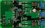
5 Assembly Drawing and PCB Layout
Figure 5-1 through Figure 5-5 show the assembly drawing and each layer.
Figure 5-1. Top Assembly
Figure 5-2. Top Layer
8
TPS51020 Buck Controller Evaluation Module User's Guide
Copyright © 2022 Texas Instruments Incorporated
SLUU194A – MAY 2004 – REVISED MARCH 2022
Submit Document Feedback
�www.ti.com
Assembly Drawing and PCB Layout
Figure 5-3. Inner Layer 1
Figure 5-4. Inner Layer 2
SLUU194A – MAY 2004 – REVISED MARCH 2022
Submit Document Feedback
TPS51020 Buck Controller Evaluation Module User's Guide
Copyright © 2022 Texas Instruments Incorporated
9
�Assembly Drawing and PCB Layout
www.ti.com
Figure 5-5. Bottom Layer
10
TPS51020 Buck Controller Evaluation Module User's Guide
Copyright © 2022 Texas Instruments Incorporated
SLUU194A – MAY 2004 – REVISED MARCH 2022
Submit Document Feedback
�www.ti.com
Circuit Module List of Materials
6 Circuit Module List of Materials
RERERENCE
DESIGNATOR
QTY
DESCRIPTION
SIZE
MFR
PART NUMBER
C1, C4, C12, C13, C16,
C17
6
Capacitor, ceramic, 2.2 mF, 25 V, X5R, 10%
1210
Panasonic
ECJ−4YB1E225K
C2, C15
2
Capacitor, ceramic, 6800 pF, 25 V, X7R, 10%
805
Std
Std
C3, C11, C19, C25
0
Capacitor, ceramic, TBD
805
Std
Std
C24
1
Capacitor, ceramic, 4.7 mF,25 V, X5R, 10%
805
Panasonic
ECJ−2FB1E475M
C22
1
Capacitor, ceramic, 3300 pF, 25 V, X7R, 5%
805
Std
Std
C14
1
Capacitor, aluminum solid cap, with conductive
polymer 22 mF, 35 V, 20%
8.3m (E7)
Sanyo
35SVPD22M
C5
1
Capacitor, ceramic, 3900 pF, 25 V, X7R, 5%
805
Std
Std
C6, C18, C27
3
Capacitor, ceramic, 0.1 mF,25 V, X7R, 10%
805
Std
Std
C7, C26
2
Capacitor, aluminum, 150 mF, 6.3 V, 20% (UE
Series)
7343
Panasonic
EEF−UE0J151R
C8, C20
0
Capacitor, aluminum, 150 mF, 6.3 V, 20% (UE
Series)
7343
Panasonic
EEF−UE0J151R
C9, C10, C21, C23
4
Capacitor, ceramic, 0.01 mF, 25 V, X7R, 10%
805
Std
Std
L1, L2
2
Inductor, SMT, 4.0 mH,10.3 A, 8.0 mW
0.492 sq”
Sumida
CEP125(H)−4R0
ShortsJumper
3
STC02SYAN
Shorts Jumper
Sullins
N/A
JP, JP2, JP3
3
Header, 3 pin, 100-mil spacing (36-pin strip)
0.100´ 3
Sullins
PTC36SAAN
R1, R9
2
Resistor, chip, 49.9 W,1/10−W, 1%
805
Vishay
Std
R10, R18
2
Resistor, chip, 1M W,1/10W, 1%
805
Vishay
Std
R4
1
Resistor,chip, 1.82 kW,1/10W, 1%
805
Vishay
Std
R21
1
Resistor, chip, 2.74 kW,1/10W, 1%
805
Vishay
Std
R11
1
Resistor, chip, 3.92 kW,1/10W, 1%
805
Vishay
Std
R2, R24
2
Resistor, chip, 10.0 kW,1/10W, 1%
805
Vishay
Std
R7, R26
2
Resistor, chip, 15 W,1/10W, 1%
805
Vishay
Std
R12, R13
2
Resistor, chip, 18.2 kW,1/10W, 1%
805
Vishay
Std
R22
1
Resistor, chip, 28.7 kW,1/10W, 1%
805
Vishay
Std
R5
1
Resistor, chip, 48.7 kWs,1/10W, 1%
805
Vishay
Std
R14,R15, R16, R27
4
Resistor, chip, 100 kW,1/10W, 1%
805
Vishay
Std
R3, R25
2
Resistor, chip, 332 W,1/10W, 1%
805
Vishay
Std
R8, R19
2
Resistor, chip, 0 W,1/10W, 1%
805
Vishay
Std
J1, J2, J3
3
Terminal block, 2 pin, 15 A, 5.1 mm
0.40´ 0.35
OST
ED1609
TP1,TP3, TP6, TP8,
TP10
5
Test point, 0.062 hole, red
0.25
Keystone
5011
TP2, TP4, TP5, TP7,
TP9, TP14
6
Test point, 0.062 hole, black
0.25
Keystone
5010
U1
1
Dual voltage mode, DDR selectable,
synchronous, step-down controller for notebook
TSSOP30
TI
TPS51020DBT
TP11,T12, TP13
3
Adaptor, 3.5-mm probe clip (or 131−5031−00)
0.2
Tektronix
131−4244−00
Q1, Q6
2
Transistor, MOSFET, N-channel, 30 V, 8.4 A, Rds SO−8
22 mW
Fairchild
FDS6612A
Q2, Q4
2
Transistor, MOSFET, N-channel, 30 V, 10 A, Rds
16 mW
SO−8
Fairchild
FDS6690S
Q3, Q5
0
Transistor, MOSFET, N-channel, 30 V, 10 A, Rds
16 mW
SO−8
Fairchild
FDS6690S
SLUU194A – MAY 2004 – REVISED MARCH 2022
Submit Document Feedback
TPS51020 Buck Controller Evaluation Module User's Guide
Copyright © 2022 Texas Instruments Incorporated
11
�References
www.ti.com
7 References
Texas Instruments, TPS51020 Dual, Voltage Mode, DDR Selectable, Synchronous, Step−down Controller for
Notebook System
8 Revision History
NOTE: Page numbers for previous revisions may differ from page numbers in the current version.
Changes from Revision * (May 2004) to Revision A (March 2022)
Page
• Updated the numbering format for tables, figures, and cross-references throughout the document. ................2
• Updated the user's guide title............................................................................................................................. 2
12
TPS51020 Buck Controller Evaluation Module User's Guide
Copyright © 2022 Texas Instruments Incorporated
SLUU194A – MAY 2004 – REVISED MARCH 2022
Submit Document Feedback
�IMPORTANT NOTICE AND DISCLAIMER
TI PROVIDES TECHNICAL AND RELIABILITY DATA (INCLUDING DATA SHEETS), DESIGN RESOURCES (INCLUDING REFERENCE
DESIGNS), APPLICATION OR OTHER DESIGN ADVICE, WEB TOOLS, SAFETY INFORMATION, AND OTHER RESOURCES “AS IS”
AND WITH ALL FAULTS, AND DISCLAIMS ALL WARRANTIES, EXPRESS AND IMPLIED, INCLUDING WITHOUT LIMITATION ANY
IMPLIED WARRANTIES OF MERCHANTABILITY, FITNESS FOR A PARTICULAR PURPOSE OR NON-INFRINGEMENT OF THIRD
PARTY INTELLECTUAL PROPERTY RIGHTS.
These resources are intended for skilled developers designing with TI products. You are solely responsible for (1) selecting the appropriate
TI products for your application, (2) designing, validating and testing your application, and (3) ensuring your application meets applicable
standards, and any other safety, security, regulatory or other requirements.
These resources are subject to change without notice. TI grants you permission to use these resources only for development of an
application that uses the TI products described in the resource. Other reproduction and display of these resources is prohibited. No license
is granted to any other TI intellectual property right or to any third party intellectual property right. TI disclaims responsibility for, and you
will fully indemnify TI and its representatives against, any claims, damages, costs, losses, and liabilities arising out of your use of these
resources.
TI’s products are provided subject to TI’s Terms of Sale or other applicable terms available either on ti.com or provided in conjunction with
such TI products. TI’s provision of these resources does not expand or otherwise alter TI’s applicable warranties or warranty disclaimers for
TI products.
TI objects to and rejects any additional or different terms you may have proposed. IMPORTANT NOTICE
Mailing Address: Texas Instruments, Post Office Box 655303, Dallas, Texas 75265
Copyright © 2022, Texas Instruments Incorporated
�