Product
Folder
Sample &
Buy
Support &
Community
Tools &
Software
Technical
Documents
TPS51100
SLUS600E – APRIL 2004 – REVISED DECEMBER 2014
TPS51100 3-A Sink / Source DDR Termination Regulator
1 Features
3 Description
•
•
•
The TPS51100 is a 3-A, sink/source tracking
termination regulator. The device is specifically
designed for low-cost and low-external component
count systems where space is a premium.
1
•
•
•
•
•
•
•
•
•
•
Input Voltage Range: 4.75 V to 5.25 V
VLDOIN Voltage Range: 1.2 V to 3.6 V
3-A Sink/Source Termination Regulator Includes
Droop Compensation
Requires Only 20-μF Ceramic Output Capacitance
Supports Hi-Z in S3 and Soft-Off in S5
1.2-V Input (VLDOIN) Helps Reduce Total Power
Dissipation
Integrated Divider Tracks 0.5 VDDQSNS for VTT
and VTTREF
Remote Sensing (VTTSNS)
±20-mV Accuracy for VTT and VTTREF
10-mA Buffered Reference (VTTREF)
Built-In Soft-Start, UVLO, and OCL
Thermal Shutdown
Supports JEDEC Specifications
The TPS51100 maintains fast transient response,
only requiring 20 μF (2 × 10 μF) of ceramic output
capacitance. The TPS51100 supports remote sensing
functions and all features required to power the DDR
and DDR2 VTT bus termination according to the
JEDEC specification. The part also supports DDR3
VTT termination with VDDQ at 1.5 V (typical). In
addition, the TPS51100 includes integrated sleepstate controls, placing VTT in Hi-Z in S3 (suspend to
RAM) and soft-off for VTT and VTTREF in S5
(suspend to disk). The TPS51100 is available in the
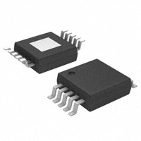
thermally efficient 10-pin MSOP PowerPAD™
package and is specified from –40°C to 85°C.
Device Information(1)
PART NUMBER
PACKAGE
BODY SIZE (NOM)
HVSSOP (10)
3.00 mm x 3.00 mm
2 Applications
TPS51100
•
•
(1) For all available packages, see the orderable addendum at
the end of the datasheet.
DDR, DDR2, DDR3 Memory Termination
SSTL-2, SSTL-18, and HSTL Termination
Simplified Schematic
TPS51100DGQ
C1
2 x 10 µF
1
VDDQSNS
2
VLDOIN
3
VTT
5V_IN
VIN 10
S5
9
GND
8
S5
C2
0.1 µF
4
PGND
5
VTTSNS
S3
7
VTTREF
6
Capacitor Manuf
S3
VTTREF
Part Number
C1
TDK
C2012JB0J106K
C2
TDK
C1608JB1H104K
1
An IMPORTANT NOTICE at the end of this data sheet addresses availability, warranty, changes, use in safety-critical applications,
intellectual property matters and other important disclaimers. PRODUCTION DATA.
�TPS51100
SLUS600E – APRIL 2004 – REVISED DECEMBER 2014
www.ti.com
Table of Contents
1
2
3
4
5
6
7
Features ..................................................................
Applications ...........................................................
Description .............................................................
Revision History.....................................................
Pin Configuration and Functions .........................
Specifications.........................................................
1
1
1
2
3
4
6.1
6.2
6.3
6.4
6.5
4
4
4
5
7
Absolute Maximum Ratings ......................................
Recommended Operating Conditions.......................
Thermal Information ..................................................
Electrical Characteristics...........................................
Typical Characteristics ..............................................
Detailed Description ............................................ 11
7.1 Overview ................................................................. 11
7.2 Functional Block Diagram ....................................... 11
7.3 Feature Description................................................. 11
7.4 Device Functional Modes........................................ 12
8
Application and Implementation ........................ 13
8.1 Application Information............................................ 13
8.2 Typical Application ................................................. 13
9 Power Supply Recommendations...................... 16
10 Layout................................................................... 16
10.1 Layout Guidelines ................................................. 16
10.2 Layout Example .................................................... 17
10.3 Thermal Considerations ........................................ 17
11 Device and Documentation Support ................. 19
11.1
11.2
11.3
11.4
Device Support......................................................
Trademarks ...........................................................
Electrostatic Discharge Caution ............................
Glossary ................................................................
19
19
19
19
12 Mechanical, Packaging, and Orderable
Information ........................................................... 19
4 Revision History
NOTE: Page numbers for previous revisions may differ from page numbers in the current version.
Changes from Revision D (May 2012) to Revision E
•
Added Pin Configuration and Functions section, Feature Description section, Device Functional Modes, Application
and Implementation section, Power Supply Recommendations section, Layout section, Device and Documentation
Support section, and Mechanical, Packaging, and Orderable Information section ............................................................... 1
Changes from Revision C (June 2008) to Revision D
•
2
Page
Page
Added updated Thermal data ................................................................................................................................................. 4
Submit Documentation Feedback
Copyright © 2004–2014, Texas Instruments Incorporated
Product Folder Links: TPS51100
�TPS51100
www.ti.com
SLUS600E – APRIL 2004 – REVISED DECEMBER 2014
5 Pin Configuration and Functions
DGQ Package
(Top View)
VDDQSNS
1
10
VIN
VLDOIN
2
9
S5
VTT
3
8
GND
PGND
4
7
S3
VTTSNS
5
6
VTTREF
Actual Size
3,05 mm x 4,98 mm
P0083-01
NOTE: For more information on the DGQ package, see the PowerPAD Thermally Enhanced Package application report
(SLMA002).
Pin Functions
PIN
NAME
NO.
I/O
DESCRIPTION
GND
8
–
Signal ground. Connect to negative terminal of the output capacitor
PGND
4
–
Power ground output for the VTT LDO
S3
7
I
S3 signal input
S5
9
I
S5 signal input
VDDQSNS
1
I
VDDQ sense input
VIN
10
I
5-V power supply
VLDOIN
2
I
Power supply for the VTT LDO and VTTREF output stage
VTT
3
O
Power output for the VTT LDO
VTTREF
6
O
VTT reference output. Connect to GND through 0.1-μF ceramic capacitor.
VTTSNS
5
I
Voltage sense input for the VTT LDO. Connect to plus terminal of the output capacitor.
Submit Documentation Feedback
Copyright © 2004–2014, Texas Instruments Incorporated
Product Folder Links: TPS51100
3
�TPS51100
SLUS600E – APRIL 2004 – REVISED DECEMBER 2014
www.ti.com
6 Specifications
6.1 Absolute Maximum Ratings
over operating free-air temperature range (unless otherwise noted) (1)
Input voltage (2)
Output voltage (2)
MIN
MAX
VIN, VLDOIN, VTTSNS, VDDQSNS, S3, S5
–0.3
6
PGND
–0.3
0.3
VTT, VTTREF
UNIT
V
–0.3
6
V
TA
Operating ambient temperature
–40
85
°C
Tstg
Storage temperature
–55
150
°C
(1)
(2)
Stresses beyond those listed under Absolute Maximum Ratings may cause permanent damage to the device. These are stress ratings
only, and functional operation of the device at these or any other conditions beyond those indicated under RecommendedOperating
Conditions is not implied. Exposure to absolute-maximum-rated conditions for extended periods may affect device reliability.
All voltage values are with respect to the network ground terminal unless otherwise noted.
6.2 Recommended Operating Conditions
over operating free-air temperature range (unless otherwise noted)
VIN
Supply voltage
TA
MAX
UNIT
V
4.75
5.25
–0.10
5.25
VLDOIN, VDDQSNS, VTT, VTTSNS
–0.1
3.6
VTTREF
–0.1
1.8
PGND
–0.1
0.1
–40
85
S3, S5
Voltage range
MIN
Operating free-air temperature
V
°C
6.3 Thermal Information
TPS51100
THERMAL METRIC (1)
DGQ
UNIT
10 PINS
RθJA
Junction-to-ambient thermal resistance
60.3
RθJC(top)
Junction-to-case (top) thermal resistance
63.5
RθJB
Junction-to-board thermal resistance
51.6
ψJT
Junction-to-top characterization parameter
1.5
ψJB
Junction-to-board characterization parameter
22.3
RθJC(bot)
Junction-to-case (bottom) thermal resistance
9.5
(1)
4
°C/W
For more information about traditional and new thermal metrics, see the IC Package Thermal Metrics application report, SPRA953.
Submit Documentation Feedback
Copyright © 2004–2014, Texas Instruments Incorporated
Product Folder Links: TPS51100
�TPS51100
www.ti.com
SLUS600E – APRIL 2004 – REVISED DECEMBER 2014
6.4 Electrical Characteristics
TA = –40°C to 85°C, VVIN = 5 V, VLDOIN and VDDQSNS are connected to 2.5 V (unless otherwise noted)
PARAMETER
TEST CONDITIONS
MIN
TYP
MAX
UNIT
0.25
0.5
1
mA
25
50
80
μA
0.3
1
μA
1.2
2
mA
6
10
μA
0.3
1
μA
SUPPLY CURRENT
IVIN
Supply current, VIN
TA = 25°C, VVIN = 5 V, no load, VS3 = VS5 = 5 V
IVINSTB
Standby currrent, VIN
TA = 25°C, VVIN = 5 V, no load, VS3 = 0 V, VS5 = 5 V
IVINSDN
Shutdown current, VIN
TA = 25°C, VVIN = 5 V, no load, VS3 = VS5 = 0 V, VVLDOIN
= VVDDQSNS = 0 V
IVLDOIN
Supply current, VLDOIN
IVLDOINSTB
Standby currrent, VLDOIN
TA = 25°C, VVIN = 5 V, no load,VS3 = 0 V, VS5 = 5 V
IVLDOINSDN
Shutdown current, VLDOIN
TA = 25°C, VVIN = 5 V, no load, VS3 = VS5 = 0 V
TA = 25°C, VVIN = 5 V, no load, VS3 = VS5 = 5 V
0.7
INPUT CURRENT
IVDDQSNS
Input current, VDDQSNS
VVIN = 5 V, VS3 = VS5 = 5 V
1
3
5
μA
IVTTSNS
Input current, VTTSNS
VVIN = 5 V, VS3 = VS5 = 5 V
–1
–0.25
1
μA
VTT OUTPUT
VVLDOIN = VVDDQSNS = 2.5 V
VVTTSNS
Output voltage, VTT
VVTTTOL25
VVTTTOL18
Output votlage tolerance to VTTREF, VTT
VVTTTOL15
IVTTOCLSRC
Source current limit, VTT
1.25
VVLDOIN = VVDDQSNS = 1.8 V
0.9
VVLDOIN = VVDDQSNS = 1.5 V
0.75
VVLDOIN = VVDDQSNS = 2.5 V, |IVTT| = 0 A
–20
20
VVLDOIN = VVDDQSNS = 2.5 V, |IVTT| = 1.5 A
–30
30
VVLDOIN = VVDDQSNS = 2.5 V, |IVTT| = 3 A
–40
40
VVLDOIN = VVDDQSNS = 1.8 V, |IVTT| = 0 A
–20
20
VVLDOIN = VVDDQSNS = 1.8 V, |IVTT| = 1 A
–30
30
VVLDOIN = VVDDQSNS = 1.8 V, |IVTT| = 2 A
–40
40
VVLDOIN = VVDDQSNS = 1.5 V, |IVTT| = 0 A
–20
20
VVLDOIN = VVDDQSNS = 1.5 V, |IVTT| = 1 A
–30
30
æV
VTT = çç VDDQSNS
2
è
ö
÷÷ ´ 0.95,
ø
PGOOD = High
Sink current limit, VTT
æV
VTT = çç VDDQSNS
2
è
3.8
6
1.5
2.2
3
3
3.6
6
1.5
2.2
3
–1
0.5
10
μA
TA = 25°C
–1
0.01
1
μA
VS3 = VS5 = 0 V,
VVTT = 0.5 V
10
17
ö
÷÷ ´ 1.05,
ø
PGOOD = High
VVTT = VVDDQ
IVTTLK
Leakage current, VTT
VTT
æV
ö
= çç VDDQSNS ÷÷ ´ 1.25 V,
2
è
ø
VS3 = 0 V,
IVTTSNSLK
Leakage current, VTTSNS
æV
VTT = çç VDDQSNS
2
è
IDSCHRG
Discharge current, VTT
TA = 25°C,
VVDDQSNS = 0 V,
mV
3
VVTT = 0 V
IVTTOCLSNK
V
TA = 25°C
A
A
VS5 = 5 V
ö
÷÷ ´ 1.25 V,
ø
mA
VTTREF OUTPUT
VVTTREF
VVTTREFTOL25
VVTTREFTOL18
Output voltage tolerance to VDDQSNS/2,
VTTREF
VVTTREFTOL15
IVTTREFOCL
VVDDQSNS
Output voltage, VTTREF
Source current limit, VTTREF
V
2
VVLDOIN = VVDDQSNS = 2.5 V, IVTTREF < 10 mA
–20
20
VVLDOIN = VVDDQSNS = 1.8 V, IVTTREF < 10 mA
–17
17
VVLDOIN = VVDDQSNS = 1.5 V, IVTTREF < 10 mA
–15
15
VVTTREF = 0 V
10
20
30
Submit Documentation Feedback
Copyright © 2004–2014, Texas Instruments Incorporated
Product Folder Links: TPS51100
mV
mA
5
�TPS51100
SLUS600E – APRIL 2004 – REVISED DECEMBER 2014
www.ti.com
Electrical Characteristics (continued)
TA = –40°C to 85°C, VVIN = 5 V, VLDOIN and VDDQSNS are connected to 2.5 V (unless otherwise noted)
PARAMETER
TEST CONDITIONS
MIN
TYP
MAX
UNIT
UVLO/LOGIC THRESHOLD
Wake up
VVINUV
UVLO threshold voltage, VIN
VIH
High-level input voltage
S3, S5
VIL
Low-level input voltage
S3, S5
VIHYST
Hysteresis voltage
S3, S5
IILEAK
Logic input leakage current
S2, S5,
Hysteresis
3.4
3.7
4
0.15
0.25
0.35
1.6
V
0.3
V
1
μA
0.2
TA = 25°C
V
–1
V
THERMAL SHUTDOWN
TSDN
6
Thermal shutdown threshold
Shutdown temperature
Hysteresis
Submit Documentation Feedback
160
10
°C
Copyright © 2004–2014, Texas Instruments Incorporated
Product Folder Links: TPS51100
�TPS51100
www.ti.com
SLUS600E – APRIL 2004 – REVISED DECEMBER 2014
1.0
2.0
0.9
1.8
IVINSDN − VINSDN Supply Current − mA
IVIN − VIN Supply Current − mA
6.5 Typical Characteristics
0.8
0.7
0.6
0.5
0.4
0.3
0.2
0
50
100
0.8
0.6
0.4
G001
0
50
100
150
G002
Figure 2. VIN Shutdown Current vs Temperature
2.0
10
1.9
DDR2
VVTT = 1.8 V
IVLDOIN − VLDOIN Supply Current − mA
IVIN − VIN Supply Current − mA
1.0
TJ − Junction Temperature − °C
Figure 1. VIN Supply Current vs Temperature
8
7
6
5
4
3
2
1
1.8
1.7
1.6
1.5
1.4
1.3
1.2
1.1
1.0
0.9
0.8
0
−2.0 −1.5 −1.0
−0.5
0.0
0.5
1.0
IVTT − VTT Load Current − A
1.5
0.7
−50
2.0
0
50
100
TJ − Junction Temperature − °C
G003
Figure 3. VIN Supply Current vs VTT Load Current
150
G004
Figure 4. VLDOIN Supply Current vs Temperature
2.0
30
1.8
IDSCHRG − VTT Discharge Current − mA
IVLDOINSDN − VLDOINSDN Supply Current − mA
1.2
0.0
−50
150
TJ − Junction Temperature − °C
9
1.4
0.2
0.1
0.0
−50
1.6
1.6
1.4
1.2
1.0
0.8
0.6
0.4
25
20
15
0.2
0.0
−50
0
50
100
TJ − Junction Temperature − °C
150
10
−50
Figure 5. VLDOIN Shutdown Current vs Temperature
0
50
100
TJ − Junction Temperature − °C
G005
150
G006
Figure 6. Discharge Current vs Temperature
Submit Documentation Feedback
Copyright © 2004–2014, Texas Instruments Incorporated
Product Folder Links: TPS51100
7
�TPS51100
SLUS600E – APRIL 2004 – REVISED DECEMBER 2014
www.ti.com
1.29
0.94
1.28
0.93
1.27
0.92
VVTT − VTT Voltage − V
VVTT − VTT Voltage − V
Typical Characteristics (continued)
1.26
1.25
VVLDOIN = 2.5 V
1.24
1.23
0.91
0.90
VVLDOIN = 1.8 V
0.89
0.88
VVLDOIN = 1.2 V
VVLDOIN = 1.8 V
1.22
0.87
VVLDOIN = 1.5 V
1.21
0.86
−4
−3
−2
−1
0
1
2
3
4
IVTT − VTT Load Current − A
−4
−3
−2
Figure 7. VTT Voltage Load Regulation vs VTT Load Current
(DDR)
−1
0
1
2
3
IVTT − VTT Load Current − A
G007
4
G008
Figure 8. VTT Voltage Load Regulation vs VTT Load Current
(DDR2)
0.79
1.252
VVLDOIN = 1.5 V
VVTTREF − VTTREF Voltage − V
0.78
VVTT − VTT Voltage − V
0.77
0.76
0.75
0.74
0.73
1.251
1.250
1.249
0.72
0.71
1.248
−3
−2
−1
0
1
2
IVTT − VTT Load Current − A
3
0
G009
Figure 9. VTT Voltage Load Regulation vs VTT Load Current
(DDR3)
2
4
6
8
IVTTREF − VTTREF Load Current − mA
10
G010
Figure 10. VTTREF Voltage Load Regulation vs VTTREF
Load Current (DDR)
752
902
VVTTREF − VTTREF Voltage − mV
VVTTREF − VTTREF Voltage − mV
VVLDOIN = 1.5 V
901
900
899
750
749
748
898
0
2
4
6
8
IVTTREF − VTTREF Load Current − mA
0
10
2
4
6
8
IVTTREF − VTTREF Load Current − mA
G011
Figure 11. VTTREF Voltage Load Regulation vs VTTREF
Load Current (DDR2)
8
751
10
G012
Figure 12. VTTREF Voltage Load Regulation vs VTTREF
Load Current (DDR3)
Submit Documentation Feedback
Copyright © 2004–2014, Texas Instruments Incorporated
Product Folder Links: TPS51100
�TPS51100
www.ti.com
SLUS600E – APRIL 2004 – REVISED DECEMBER 2014
Typical Characteristics (continued)
VS3 = 0 V
IVTT = IVTTREF = 0 A
VVLDOIN (50 mV/div)
Offset: 1.8 V
VS5
(5 V/div)
VS3
(5 V/div)
VVTT (20 mV/div)
Offset 0.9 V
VVTTREF
(0.5 V/div)
VVTTREF
(20 mV/div)
Offset 0.9 V
VVTT (0.5 V/div)
IVTT
(2 A/div)
t − Time − 10 ms/div
t − Time − 20 ms/div
G013
G014
Figure 13. VTT Voltage Load Transient Response
Figure 14. Startup Waveforms S5 Low-to-High
VS5
(5 V/div)
VS3
(5 V/div)
VS5
(5 V/div)
VS3
(5 V/div)
VTTREF
VVTTREF
(0.5 V/div)
VVTT
(0.5 V/div)
VVTT
(0.5 V/div)
VS5 = 5 V
IVTT = IVTTREF = 0 A
VS5 = 5 V
IVTT = IVTTREF = 0 A
t − Time − 1 ms/div
t − Time − 10 ms/div
G016
G015
Figure 16. Shutdown Waveforms S3 High-to-Low
Figure 15. Startup Waveforms S3 Low-to-High
180
80
Phase
(−1 A)
60
Gain − dB
VS3
(5 V/div)
VTTREF
(0.5 V/div)
135
Phase
(−0.1 A)
40
90
20
45
0
Gain
(−0.1 A)
0
−20
VVTT
(0.5 V/div)
−45
C1 = 2 × 10 mF
−40
10k
100k
IVTT = IVTTREF = 0 A
t − Time − 1 ms/div
Phase − °
VS5
(5 V/div)
Gain
(−1 A)
1M
−90
10M
f − Frequency − Hz
G018
G017
Figure 17. Shutdown Waveforms S3 and S5 High-to-Low
Figure 18. Bode Plot DDR Source
Submit Documentation Feedback
Copyright © 2004–2014, Texas Instruments Incorporated
Product Folder Links: TPS51100
9
�TPS51100
SLUS600E – APRIL 2004 – REVISED DECEMBER 2014
www.ti.com
Typical Characteristics (continued)
180
80
60
180
80
Phase
(−1 A)
Phase
(1 A)
135
135
60
Phase
(−0.1 A)
Gain
(0.1 A)
−20
C1 = 2 × 10 mF
−40
10k
100k
0
Gain
(−1 A)
C1 = 2 × 10 mF
−40
10k
100k
−90
10M
1M
45
Gain
(−0.1 A)
−20
−45
Gain
(1 A)
20
0
0
90
Phase − °
45
Phase
(0.1 A)
Gain − dB
20
0
40
90
Phase − °
Gain − dB
40
f − Frequency − Hz
1M
−45
−90
10M
f − Frequency − Hz
G019
G020
Figure 19. Bode Plot DDR Sink
Figure 20. Bode Plot DDR2 Source
180
80
60
135
40
90
20
0
45
Phase
(0.1 A)
Gain
(0.1 A)
−20
0
−45
Gain
(1 A)
C1 = 2 × 10 mF
−40
10k
100k
Phase − °
Gain − dB
Phase
(1 A)
1M
−90
10M
f − Frequency − Hz
G021
Figure 21. Bode Plot DDR2 Sink
10
Submit Documentation Feedback
Copyright © 2004–2014, Texas Instruments Incorporated
Product Folder Links: TPS51100
�TPS51100
www.ti.com
SLUS600E – APRIL 2004 – REVISED DECEMBER 2014
7 Detailed Description
7.1 Overview
The TPS51100 is a sink / source double date rate (DDR) termination regulator with VTTREF buffered reference
output.
7.2 Functional Block Diagram
VDDQSNS
1
+
VLDOIN
6
VTTREF
3
VTT
4
PGND
HalfDDQ
+
–
–
GND
2
8
VIN 10
+
3.7 V/3.5 V
VTTSNS
5
S3
7
VinOK
ENREF
–
+
–
ENVTT
ENVTT
+
5 V/10%
–
ENREF
S5
+
9
PGOOD
+
+
–
–5 V/10%
TPS51100DGQ
B0319-01
Figure 22. Simplified Block Diagram
7.3 Feature Description
7.3.1 VTT Sink/Source Regulator
The TPS51100 is a 3-A sink/source tracking termination regulator designed specially for low-cost, low-externalcomponents systems where space is at premium, such as notebook PC applications. The TPS51100 integrates a
high-performance, low-dropout linear regulator that is capable of sourcing and sinking current up to 3 A. This
VTT linear regulator employs an ultimate fast-response feedback loop so that small ceramic capacitors are
enough to keep tracking to the VTTREF within ±40 mV under all conditions, including fast load transient. To
achieve tight regulation with minimum effect of trace resistance, a remote sensing terminal, VTTSNS, should be
connected to the positive node of the VTT output capacitor(s) as a separate trace from the high-current line from
VTT.
7.3.2 VTTREF Regulator
The VTTREF block consists of an on-chip 1/2 divider, low-pass filter (LPF), and buffer. This regulator can source
current up to 10 mA. Bypass VTTREF to GND using a 0.1-μF ceramic capacitor to ensure stable operation.
Submit Documentation Feedback
Copyright © 2004–2014, Texas Instruments Incorporated
Product Folder Links: TPS51100
11
�TPS51100
SLUS600E – APRIL 2004 – REVISED DECEMBER 2014
www.ti.com
Feature Description (continued)
7.3.3 Soft-Start
The soft-start function of the VTT is achieved via a current clamp, allowing the output capacitors to be charged
with low and constant current that gives linear ramp-up of the output voltage. The current-limit threshold is
changed in two stages using an internal powergood signal. When VTT is outside the powergood threshold, the
current limit level is 2.2 A. When VTT rises above (VTTREF – 5%) or falls below (VTTREF + 5%), the current
limit level switches to 3.8 A. The thresholds are typically VTTREF ±5% (from outside regulation to inside) and
±10% (when it falls outside). The soft-start function is completely symmetrical, and it works not only from GND to
VTTREF voltage, but also from VDDQ to VTTREF voltage. Note that the VTT output is in a high-impedance state
during the S3 state (S3 = low, S5 = high), and its voltage can be up to VDDQ voltage, depending on the external
condition. Note that VTT does not start under a full-load condition.
7.3.4 VTT Current Protection
The LDO has a constant overcurrent limit (OCL) at 3.8 A. This trip point is reduced to 2.2 A before the output
voltage comes within ±5% of the target voltage or goes outside of ±10% of the target voltage.
7.3.5 VIN UVLO Protection
For VIN undervoltage lockout (UVLO) protection, the TPS51100 monitors VIN voltage. When the VIN voltage is
lower than UVLO threshold voltage, the VTT regulator is shut off. This is a non-latch protection.
7.3.6 Thermal Shutdown
TPS51100 monitors its temperature. If the temperature exceeds the threshold value, typically 160°C, the VTT
and VTTREF regulators are shut off. This is also a non-latch protection.
7.4 Device Functional Modes
7.4.1 S5 Control and Soft-Off
The S3 and S5 terminals should be connected to SLP_S3 and SLP_S5 signals, respectively. Both VTTREF and
VTT are turned on at the S0 state (S3 = high, S5 = high). VTTREF is kept alive while VTT is turned off and left
high-impedance in the S3 state (S3 = low, S5 = high). Both VTT and VTTREF outputs are turned off and
discharged to ground through internal MOSFETs during S4/S5 state (both S3 and S5 are low).
Table 1. S3 and S5 Control Table
(1)
12
STATE
S3
S5
VTTREF
VTT
S0
H
H
1
1
S3 (1)
L
H
1
0 (Hi-Z)
S4/S5 (1)
L
L
0 (discharge)
0 (discharge)
In case S3 is forced to H and S5 to L, VTTREF is discharged and VTT is at Hi-Z state. This condition
is not recommended.
Submit Documentation Feedback
Copyright © 2004–2014, Texas Instruments Incorporated
Product Folder Links: TPS51100
�TPS51100
www.ti.com
SLUS600E – APRIL 2004 – REVISED DECEMBER 2014
8 Application and Implementation
NOTE
Information in the following applications sections is not part of the TI component
specification, and TI does not warrant its accuracy or completeness. TI’s customers are
responsible for determining suitability of components for their purposes. Customers should
validate and test their design implementation to confirm system functionality.
8.1 Application Information
The TPS51100 is typically used as a sink / source tracking termination regulator, witch converter a voltage from
VTT.
8.2 Typical Application
TPS51100DGQ
C1
2 x 10 µF
1
VDDQSNS
2
VLDOIN
3
VTT
5V_IN
VIN 10
S5
9
GND
8
S5
C2
0.1 µF
4
PGND
5
VTTSNS
S3
7
VTTREF
6
S3
VTTREF
Capacitor Manuf
Part Number
C1
TDK
C2012JB0J106K
C2
TDK
C1608JB1H104K
Figure 23. TPS51100 5-V Input / 1.8-V Output Reference Design
8.2.1 Design Requirements
Table 2. Design Parameters
DESIGN PARAMETERS
EXAMPLE VALUE
VIN
4.75 V to 5.25 V
VDDQSNS, VLDOIN
1.8 V
Output Current
±3 A
8.2.2 Detailed Design Procedure
Table 3. Design Specifications
REFERENCE
DESIGNATOR
SPECIFICATION
MANUFACTURER
C1
10-μf, 6.3-V, X5R, 2012 (0805)
TDK
C2012JB0J106K
C2
0.1-μf, 50-V, X5R, 1608 (0603)
TDK
C1608JB1H104K
PART NUMBER
Submit Documentation Feedback
Copyright © 2004–2014, Texas Instruments Incorporated
Product Folder Links: TPS51100
13
�TPS51100
SLUS600E – APRIL 2004 – REVISED DECEMBER 2014
www.ti.com
8.2.2.1 Output Capacitor
For stable operation, total capacitance of the VTT output terminal can be equal to or greater than 20 μF. Attach
two 10-μF ceramic capacitors in parallel to minimize the effect of ESR and ESL. If the ESR is greater than 2 mΩ,
insert an R-C filter between the output and the VTTSNS input to achieve loop stability. The R-C filter time
constant should be almost the same or slightly lower than the time constant of the output capacitor and its ESR.
Soft-start duration, tSS, is also a function of this output capacitance. Where ITTOCL = 2.2 A (typ), tSS can be
calculated as,
æC
´ VVTT ö
t SS = ç OUT
÷
è IVTTOCL ø
(1)
8.2.2.2 Input Capacitor
Depending on the trace impedance between the VLDOIN bulk power supply to the part, transient increase of
source current is supplied mostly by the charge from the VLDOIN input capacitor. Use a 10-μF (or more) ceramic
capacitor to supply this transient charge. Provide more input capacitance as more output capacitance is used at
VTT. In general, use 1/2 COUT for the input.
8.2.2.3 VIN Capacitor
Add a ceramic capacitor with a value between 1 μF and 4.7 μF placed close to the VIN pin, to stabilize 5 V from
any parasitic impedance from the supply.
8.2.3 Application Curves
VS3 = 0 V
IVTT = IVTTREF = 0 A
VS5
(5 V/div)
VS5
(5 V/div)
VS3
(5 V/div)
VS3
(5 V/div)
VTTREF
VVTTREF
(0.5 V/div)
VVTT (0.5 V/div)
VVTT
(0.5 V/div)
VS5 = 5 V
IVTT = IVTTREF = 0 A
t − Time − 10 ms/div
t − Time − 10 ms/div
G014
Figure 24. Start-Up Waveforms S5 Low-to-High
14
G015
Figure 25. Start-Up Waveforms S3 Low-to-High
Submit Documentation Feedback
Copyright © 2004–2014, Texas Instruments Incorporated
Product Folder Links: TPS51100
�TPS51100
www.ti.com
SLUS600E – APRIL 2004 – REVISED DECEMBER 2014
VS3
(5 V/div)
VS5
(5 V/div)
VVTTREF
(0.5 V/div)
VVTT
(0.5 V/div)
VS5 = 5 V
IVTT = IVTTREF = 0 A
t − Time − 1 ms/div
G016
Figure 26. Shutdown Waveforms S3 High-to-Low
Submit Documentation Feedback
Copyright © 2004–2014, Texas Instruments Incorporated
Product Folder Links: TPS51100
15
�TPS51100
SLUS600E – APRIL 2004 – REVISED DECEMBER 2014
www.ti.com
9 Power Supply Recommendations
TPS51100 is designed for a sink / source double date rate (DDR) termination regulator with VTTREF buffered
reference output. Supply input voltage (VIN) support voltage from 4.75 V to 5.25 V; VLDOIN input voltage
supports from 1.2 V to 3.6 V.
10 Layout
10.1 Layout Guidelines
Consider the following points before the layout of TPS51100 design begins.
• The input bypass capacitor for VLDOIN should be placed to the pin as close as possible with a short and
wide connection.
• The output capacitor for VTT should be placed close to the pin with a short and wide connection in order to
avoid additional ESR and/or ESL of the trace.
• VTTSNS should be connected to the positive node of VTT output capacitor(s) as a separate trace from the
high current power line and is strongly recommended to avoid additional ESR and/or ESL. If it is needed to
sense the voltage of the point of the load, it is recommended to attach the output capacitor(s) at that point.
Also, it is recommended to minimize any additional ESR and/or ESL of the ground trace between the GND
pin and the output capacitor(s).
• Consider adding an LPF at VTTSNS in case the ESR of the VTT output capacitor(s) is larger than 2 mΩ.
• VDDQSNS can be connected separately from VLDOIN. Remember that this sensing potential is the reference
voltage of VTTREF. Avoid any noise generative lines.
• The negative node of the VTT output capacitor(s) and the VTTREF capacitor should be tied together,
avoiding common impedance to the high-current path of the VTT source/sink current.
• The GND (signal GND) pin node represents the reference potential for the VTTREF and VTT outputs.
Connect GND to the negative nodes of the VTT capacitor(s), VTTREF capacitor, and VDDQ capacitor(s) with
care to avoid additional ESR and/or ESL. GND and PGND (Power GND) should be isolated, with a single
point connection between them.
• In order to remove heat from the package effectively, prepare the thermal land and solder to the package
thermal pad. The wide trace of the component-side copper, connected to this thermal land, helps heat
spreading. Numerous vias 0.33 mm in diameter connected from the thermal land to the internal/solder-side
ground plane(s) should be used to help dissipation.
16
Submit Documentation Feedback
Copyright © 2004–2014, Texas Instruments Incorporated
Product Folder Links: TPS51100
�TPS51100
www.ti.com
SLUS600E – APRIL 2004 – REVISED DECEMBER 2014
10.2 Layout Example
NOTES: 1. The positive terminal of each output capacitor should be directly connected to VTT of the IC; do not use a VIA.
2. The negative terminal of each output capacitor should be directly connected to GND of the IC; do not use a VIA.
3. VIAs
VIA between 1st and 2nd layers
VIA between 1st and other layers under 2nd
4. Rs and Cs with dotted outlines are options.
Figure 27. TPS51100 PCB Layout Guideline
10.3 Thermal Considerations
As the TPS51100 is a linear regulator, the VTT current flow in both source and sink directions generates power
dissipation from the device. In the source phase, the potential difference between VVLDOIN and VVTT times VTT
current becomes the power dissipation, WDSRC.
WDSRC = (VVLDOIN - VVTT )´ IVTT
(2)
In this case, if VLDOIN is connected to an alternative power supply lower than VDDQ voltage, power loss can be
decreased.
For the sink phase, VTT voltage is applied across the internal LDO regulator, and the power dissipation, and
WDSNK, is calculated by:
WDSNK = VVTT ´ IVTT
(3)
Because the device does not sink and source the current at the same time and IVTT varies rapidly with time, the
actual power dissipation that must be considered for thermal design is an average over the thermal relaxation
duration of the system. Another power consumption is the current used for internal control circuitry from the VIN
supply and VLDOIN supply. This can be estimated as 20 mW or less at normal operational conditions. This
power must be effectively dissipated from the package. Maximum power dissipation allowed to the package is
calculated by,
WPKG =
(TJ(max) - TA(max) )
qJA
(4)
where
TJ(max) is 125°C
Submit Documentation Feedback
Copyright © 2004–2014, Texas Instruments Incorporated
Product Folder Links: TPS51100
17
�TPS51100
SLUS600E – APRIL 2004 – REVISED DECEMBER 2014
www.ti.com
Thermal Considerations (continued)
TA(max) is the maximum ambient temperature in the system
θJA is the thermal resistance from the silicon junction to the ambient
This thermal resistance strongly depends on the board layout. TPS51100 is assembled in a thermally enhanced
PowerPAD package that has an exposed die pad underneath the body. For improved thermal performance, this
die pad must be attached to the ground trace via thermal land on the PCB. This ground trace acts as a heat
sink/spread. The typical thermal resistance, 57.7°C/W, is achieved based on a 3 mm × 2 mm thermal land with
two vias without air flow. It can be improved by using larger thermal land and/or increasing the number of vias.
For example, assuming a 3 mm × 3 mm thermal land with four vias without air flow, it is 45.4°C/W. Further
information about the PowerPAD package and its recommended board layout is described in the PowerPAD
Thermally Enhanced Package application report (SLMA002). This document is available at www.ti.com.
18
Submit Documentation Feedback
Copyright © 2004–2014, Texas Instruments Incorporated
Product Folder Links: TPS51100
�TPS51100
www.ti.com
SLUS600E – APRIL 2004 – REVISED DECEMBER 2014
11 Device and Documentation Support
11.1 Device Support
11.1.1 Third-Party Products Disclaimer
TI'S PUBLICATION OF INFORMATION REGARDING THIRD-PARTY PRODUCTS OR SERVICES DOES NOT
CONSTITUTE AN ENDORSEMENT REGARDING THE SUITABILITY OF SUCH PRODUCTS OR SERVICES
OR A WARRANTY, REPRESENTATION OR ENDORSEMENT OF SUCH PRODUCTS OR SERVICES, EITHER
ALONE OR IN COMBINATION WITH ANY TI PRODUCT OR SERVICE.
11.2 Trademarks
PowerPAD is a trademark of Texas Instruments.
All other trademarks are the property of their respective owners.
11.3 Electrostatic Discharge Caution
These devices have limited built-in ESD protection. The leads should be shorted together or the device placed in conductive foam
during storage or handling to prevent electrostatic damage to the MOS gates.
11.4 Glossary
SLYZ022 — TI Glossary.
This glossary lists and explains terms, acronyms, and definitions.
12 Mechanical, Packaging, and Orderable Information
The following pages include mechanical, packaging, and orderable information. This information is the most
current data available for the designated devices. This data is subject to change without notice and revision of
this document. For browser-based versions of this data sheet, refer to the left-hand navigation.
Submit Documentation Feedback
Copyright © 2004–2014, Texas Instruments Incorporated
Product Folder Links: TPS51100
19
�PACKAGE OPTION ADDENDUM
www.ti.com
10-Dec-2020
PACKAGING INFORMATION
Orderable Device
Status
(1)
Package Type Package Pins Package
Drawing
Qty
Eco Plan
(2)
Lead finish/
Ball material
MSL Peak Temp
Op Temp (°C)
Device Marking
(3)
(4/5)
(6)
TPS51100DGQ
ACTIVE
HVSSOP
DGQ
10
80
RoHS & Green
NIPDAUAG
Level-1-260C-UNLIM
-40 to 85
51100
TPS51100DGQG4
ACTIVE
HVSSOP
DGQ
10
80
RoHS & Green
NIPDAUAG
Level-1-260C-UNLIM
-40 to 85
51100
TPS51100DGQR
ACTIVE
HVSSOP
DGQ
10
2500
RoHS & Green NIPDAU | NIPDAUAG
Level-1-260C-UNLIM
-40 to 85
51100
TPS51100DGQRG4
ACTIVE
HVSSOP
DGQ
10
2500
RoHS & Green
Level-1-260C-UNLIM
-40 to 85
51100
NIPDAU
(1)
The marketing status values are defined as follows:
ACTIVE: Product device recommended for new designs.
LIFEBUY: TI has announced that the device will be discontinued, and a lifetime-buy period is in effect.
NRND: Not recommended for new designs. Device is in production to support existing customers, but TI does not recommend using this part in a new design.
PREVIEW: Device has been announced but is not in production. Samples may or may not be available.
OBSOLETE: TI has discontinued the production of the device.
(2)
RoHS: TI defines "RoHS" to mean semiconductor products that are compliant with the current EU RoHS requirements for all 10 RoHS substances, including the requirement that RoHS substance
do not exceed 0.1% by weight in homogeneous materials. Where designed to be soldered at high temperatures, "RoHS" products are suitable for use in specified lead-free processes. TI may
reference these types of products as "Pb-Free".
RoHS Exempt: TI defines "RoHS Exempt" to mean products that contain lead but are compliant with EU RoHS pursuant to a specific EU RoHS exemption.
Green: TI defines "Green" to mean the content of Chlorine (Cl) and Bromine (Br) based flame retardants meet JS709B low halogen requirements of