www.ti.com
Table of Contents
User’s Guide
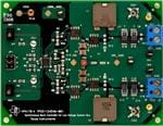
TPS51124 Buck Controller Evaluation Module User's
Guide
Table of Contents
1 Description.............................................................................................................................................................................. 2
2 Electrical Performance...........................................................................................................................................................2
3 Schematic................................................................................................................................................................................3
4 Test Setup and Results.......................................................................................................................................................... 4
4.1 Test Setup.......................................................................................................................................................................... 4
4.2 Test Procedure................................................................................................................................................................... 4
4.3 Start-Up Performance........................................................................................................................................................ 5
4.4 Transient Performance.......................................................................................................................................................5
5 Configuration.......................................................................................................................................................................... 6
5.1 Switching Frequency Selection.......................................................................................................................................... 6
5.2 Bootstrap Diode Selection..................................................................................................................................................6
6 EVM Assembly Drawing and PCB Layout............................................................................................................................ 7
7 List of Materials.....................................................................................................................................................................10
8 References.............................................................................................................................................................................11
9 Revision History....................................................................................................................................................................11
Trademarks
D-CAP™ is a trademark of Texas Instruments.
All trademarks are the property of their respective owners.
SLUU252B – APRIL 2006 – REVISED MARCH 2022
Submit Document Feedback
TPS51124 Buck Controller Evaluation Module User's Guide
Copyright © 2022 Texas Instruments Incorporated
1
�Description
www.ti.com
1 Description
The TPS51124 is a dual, adaptive on-time D-CAP™ mode synchronous buck controller. The part enables system
designers to cost-effectively complete the suite of notebook power bus regulators with the absolute lowest
external component count and lowest standby consumption. The fixed frequency emulated adaptive on-time
control supports seamless operation between PWM mode at heavy load condition and reduced frequency
operation at light load for high efficiency down to milli-ampere range. The main control loop for the TPS51124
uses D-CAP mode that is optimized for low-ESR output capacitors such as POSCAP or SP-CAP promises fast
transient response with no external compensation. Simple and separate power-good signals for each channel
allow flexibility of power sequencing. The part provides a convenient and efficient operation with supply input
voltages (V5IN, V5FILT) ranging from 4.5 V to 5.5 V, conversion voltages (drain voltage for the synchronous
high-side MOSFET) from 3 V to 28 V, and output voltages from 0.76 V to 5.5 V.
The HPA178 (TPS51124EVM) evaluation module is a high efficiency, dual synchronous buck converter providing
1.05 V at 10 A and 1.5 V at 10 A from 5-V to 25-V input. This user’s guide describes the HPA178 performance in
medium switching frequency.
2 Electrical Performance
MIN
TYP
MAX
UNIT
Input voltage range (V5IN)
SPECIFICATIONS
TEST CONDITIONS
4.5
5.0
5.5
V
Input voltage range (VIN)
5
12
25
V
Output voltage
Operating frequency
CH1
TONSEL: Float
VIN = 12 V, IOUT1 = 10 A
Output current
Overcurrent limit
VIN = 12 V
Output ripple voltage
VIN = 12 V,IOUT = 10 A
Output voltage
Operating frequency
CH2
2
TONSEL: Float
VIN = 12 V, IOUT2 = 10 A
Output current
1.05
V
300
kHz
10
A
13
A
35
mVp-p
1.5
V
360
kHz
10
A
Overcurrent limit
VIN = 12 V
13
A
Output ripple voltage
VIN = 12 V, IOUT2 = 10 A
35
mVp-p
TPS51124 Buck Controller Evaluation Module User's Guide
Copyright © 2022 Texas Instruments Incorporated
SLUU252B – APRIL 2006 – REVISED MARCH 2022
Submit Document Feedback
�www.ti.com
Schematic
3 Schematic
Figure 3-1. TPS51124 EVM Schematic Diagram
SLUU252B – APRIL 2006 – REVISED MARCH 2022
Submit Document Feedback
TPS51124 Buck Controller Evaluation Module User's Guide
Copyright © 2022 Texas Instruments Incorporated
3
�Test Setup and Results
www.ti.com
4 Test Setup and Results
4.1 Test Setup
Connect the test equipment and HPA178 EVM board as shown in Figure 4-1.
DMM4
+
-
5V/1A
Power supply
Oscilloscope
+
CH1
V5IN
_GND
V5IN
+
TP10
-
DMM1
-
CN1
TP8
+
VO1
VO1_GND
TP5
TP4
HPA178
TPS51124EVM-001
VIN
+
TP9
-
Electronic
Load1
-
TP6
CN2
VO2
TP7
DMM3
12V/10A
Power supply
TP3
VIN
_GND
VO2_GND
+
+
Electronic
Load2
CH2
Oscilloscope
DMM2
+
FAN
Figure 4-1. Equipment Setup for HPA178 EVM Board
4.2 Test Procedure
1.
2.
3.
4.
5.
6.
4
Ensure the switches SW1 (EN1) and SW2 (EN2) are in the “OFF” position.
Ensure the shunt jumper for JP1 is set 3-pin to 4-pin (Med).
Apply appropriate V5IN voltage to V5IN and V5IN_GND terminals.
Apply appropriate VIN voltage to VIN and VIN_GND terminals.
Turn on SW1 (EN1). The CH1-output will start up.
Turn on SW2 (EN2). The CH2-output will start up.
TPS51124 Buck Controller Evaluation Module User's Guide
Copyright © 2022 Texas Instruments Incorporated
SLUU252B – APRIL 2006 – REVISED MARCH 2022
Submit Document Feedback
�www.ti.com
Test Setup and Results
4.3 Start-Up Performance
Figure 4-2. 1.05-V Start-Up Performance
Figure 4-3. 1.5-V Start-Up Performance
4.4 Transient Performance
Figure 4-4. 1.05-V Load Transient Performance
SLUU252B – APRIL 2006 – REVISED MARCH 2022
Submit Document Feedback
Figure 4-5. 1.5-V Load Transient Performance
TPS51124 Buck Controller Evaluation Module User's Guide
Copyright © 2022 Texas Instruments Incorporated
5
�Configuration
www.ti.com
5 Configuration
This EVM could be set to the desired configurations of the user.
Please refer to the following specific configuration setting sections.
5.1 Switching Frequency Selection
Switching frequency can be set by the TONSEL pin using JP1 on the EVM. The default setting is medium.
Table 5-1. Switching Frequency Selection
Jumper (JP1) Set to
Frequency(1)
TONSEL
Typ
CH1
CH2
Top(1-2 pin shorted)
GND
Slow
240 kHz
300 kHz
CENTER(3-4 pin shorted)
Float
Medium
300 kHz
360 kHz
Bottom(5-6 pin shorted)
V5FILT
Fast
360 kHz
420 kHz
(1)
Frequencies are approximate.
5.2 Bootstrap Diode Selection
Bootstrap diodes (D1, D2) are not populated on this EVM since the TPS51124 has them built in. External
Schottky diodes can be added in order to further improve the efficiency.
6
TPS51124 Buck Controller Evaluation Module User's Guide
Copyright © 2022 Texas Instruments Incorporated
SLUU252B – APRIL 2006 – REVISED MARCH 2022
Submit Document Feedback
�www.ti.com
EVM Assembly Drawing and PCB Layout
6 EVM Assembly Drawing and PCB Layout
Figure 6-1. Top Assembly
Figure 6-2. Top Layer
SLUU252B – APRIL 2006 – REVISED MARCH 2022
Submit Document Feedback
TPS51124 Buck Controller Evaluation Module User's Guide
Copyright © 2022 Texas Instruments Incorporated
7
�EVM Assembly Drawing and PCB Layout
www.ti.com
Figure 6-3. Inner Layer 1
Figure 6-4. Inner Layer 2
8
TPS51124 Buck Controller Evaluation Module User's Guide
Copyright © 2022 Texas Instruments Incorporated
SLUU252B – APRIL 2006 – REVISED MARCH 2022
Submit Document Feedback
�www.ti.com
EVM Assembly Drawing and PCB Layout
Figure 6-5. Bottom Layer
SLUU252B – APRIL 2006 – REVISED MARCH 2022
Submit Document Feedback
TPS51124 Buck Controller Evaluation Module User's Guide
Copyright © 2022 Texas Instruments Incorporated
9
�List of Materials
www.ti.com
7 List of Materials
Reference
Designator
QTY
Description
Size
Mfr
Part Number
—
1
Shunt,100-mil, Black
0.100
3M
929950-00
C1
0
Capacitor,Aluminum
0.26 × 0.26 inch
Any
Any
C13, C14
2
Capacitor, POSCAP, 330 mF, 2.5V18-mW, 20%
7343
SANYO
2R5TPE330MI
C15
1
Capacitor,Ceramic, 4.7 mF,6.3 V, BJ, 0805
20%
TDK
C2012X5R0J475K
C16
1
Capacitor,Ceramic, 1 mF,6.3 V, BJ,
20%
0805
TDK
C2012X5R0J105K
C17
1
Capacitor,Ceramic, 18 pF, 50 V, BJ,
20%
0805
Std
Std
C2, C3, C4, C5
4
Capacitor,Ceramic, 10 mF,25 V, BJ ,
20%
1210
TDK /
TaiyoYuden
C3225JB1E106 /
TMK325BJ106MM
C6, C11
2
Capacitor,Ceramic, 0.1 mF,50 V, BJ,
20%
0805
Std
Std
C7, C8
2
Capacitor, POSCAP, 330 mF, 2.5V15-mW, 20%
7343
SANYO
2R5TPE330MF
C9, C10, C12, C18
0
Capacitor,Ceramic
0805
Any
Any
CN1, CN2
2
Adaptor, 3.5-mm probe clip (or
131-5031-00)
0.2
Tektronix
131-4244-00
D1, D2
0
Diode,Schottky, 0.5 A, 30 V
SOD-123
Any
Any
J1, J2
2
TerminalBlock, 2-pin, 15 A, 5.1 mm
0.40 × 0.35 inch
OST
ED1609
JP1
1
Header, 2×3-pin,100mil spacing (36- 0.20 × 0.30 inch
pin strip)
Sullins
PTC36DAAN
L1, L2
2
Inductor,1.0 μH, 20.5 A, 2 mW
TOKO
FDA1254-1R0M
Q1, Q3
2
MOSFET,N-ch, 30 V, 11 A, 12.5 mW SO8
IR
IRF7821
Q2, Q4
2
MOSFET,N-ch, 30 V, 13.8 A, 6.8 mW SO8
IR
IRF8113
R1, R7
2
Resistor,Chip, 100 kW,1/10W, 1%
0805
Std
Std
R12, R13
0
Resistor,Chip
0805
Std
Std
R2, R9, R10
3
Resistor,Chip, 3.3 W,1/10W, 1%
0805
Std
Std
R3
1
Resistor,Chip, 28.7 kW,1/10W, 1%
0805
Std
Std
R4, R6
2
Resistor,Chip, 75 kW,1/10W, 1%
0805
Std
Std
R5
1
Resistor,Chip, 73.2 kW,1/10W, 1%
0805
Std
Std
R8, R11
2
Resistor,Chip, 6.8 kW,1/10W, 1%
0805
Std
Std
SW1, SW2
2
Switch,ON-ON Mini Toggle
0.28 × 0.18 inch
Nikkai
G12AP
TP1, TP2
2
Testpoint, White, Thru hole
0.125× 0.125 inch
Keystone
5012
TP10
1
Testpoint, Orange, Thru hole
0.125× 0.125 inch
Keystone
5013
TP3, TP4, TP5, TP6
4
Testpoint, Black, Thru hole
0.125× 0.125 inch
Keystone
5011
TP7, TP8
2
Testpoint, Yellow, Thru hole
0.125× 0.125 inch
Keystone
5014
TP9
1
Testpoint, Red, Thru hole
0.125× 0.125 inch
Keystone
5010
U1
1
IC, Dual Synchronous Step-Down
Controller for Low Voltage Power
Rails
QFN32
TI
TPS51124RHB
VIN_GND,VIN,
V5IN,V5IN_GND
4
Pin,Wiring Terminal
0.09(D) × 0.31 inch
MillMax
3183-2-00-15-0000-080
10
0.496 × 0.532 inch
TPS51124 Buck Controller Evaluation Module User's Guide
Copyright © 2022 Texas Instruments Incorporated
SLUU252B – APRIL 2006 – REVISED MARCH 2022
Submit Document Feedback
�www.ti.com
References
8 References
Texas Instruments, TPS51124 Dual Synchronous Step-Down Controller for Low Voltage Power Rails Data Sheet
9 Revision History
NOTE: Page numbers for previous revisions may differ from page numbers in the current version.
Changes from Revision A (June 2008) to Revision B (March 2022)
Page
• Updated the numbering format for tables, figures, and cross-references throughout the document. ................2
• Updated the user's guide title............................................................................................................................. 2
SLUU252B – APRIL 2006 – REVISED MARCH 2022
Submit Document Feedback
TPS51124 Buck Controller Evaluation Module User's Guide
Copyright © 2022 Texas Instruments Incorporated
11
�IMPORTANT NOTICE AND DISCLAIMER
TI PROVIDES TECHNICAL AND RELIABILITY DATA (INCLUDING DATA SHEETS), DESIGN RESOURCES (INCLUDING REFERENCE
DESIGNS), APPLICATION OR OTHER DESIGN ADVICE, WEB TOOLS, SAFETY INFORMATION, AND OTHER RESOURCES “AS IS”
AND WITH ALL FAULTS, AND DISCLAIMS ALL WARRANTIES, EXPRESS AND IMPLIED, INCLUDING WITHOUT LIMITATION ANY
IMPLIED WARRANTIES OF MERCHANTABILITY, FITNESS FOR A PARTICULAR PURPOSE OR NON-INFRINGEMENT OF THIRD
PARTY INTELLECTUAL PROPERTY RIGHTS.
These resources are intended for skilled developers designing with TI products. You are solely responsible for (1) selecting the appropriate
TI products for your application, (2) designing, validating and testing your application, and (3) ensuring your application meets applicable
standards, and any other safety, security, regulatory or other requirements.
These resources are subject to change without notice. TI grants you permission to use these resources only for development of an
application that uses the TI products described in the resource. Other reproduction and display of these resources is prohibited. No license
is granted to any other TI intellectual property right or to any third party intellectual property right. TI disclaims responsibility for, and you
will fully indemnify TI and its representatives against, any claims, damages, costs, losses, and liabilities arising out of your use of these
resources.
TI’s products are provided subject to TI’s Terms of Sale or other applicable terms available either on ti.com or provided in conjunction with
such TI products. TI’s provision of these resources does not expand or otherwise alter TI’s applicable warranties or warranty disclaimers for
TI products.
TI objects to and rejects any additional or different terms you may have proposed. IMPORTANT NOTICE
Mailing Address: Texas Instruments, Post Office Box 655303, Dallas, Texas 75265
Copyright © 2022, Texas Instruments Incorporated
�