TPS51113, TPS51163
www.ti.com ....................................................................................................................................................................................................... SLUS864 – MAY 2009
SYNCHRONOUS BUCK CONTROLLER WITH HIGH-CURRENT GATE DRIVER
Check for Samples :TPS51113 TPS51163
FEATURES
DESCRIPTION
•
•
•
•
•
The TPS51113 and TPS51163 are cost-optimized,
feature rich, single-channel synchronous-buck
controllers that operates from a single 4.5-V to 13.2-V
supply and can convert an input voltage as low as
1.5 V.
1
•
•
•
•
•
Flexible Power Rails: 5 V to 12 V
Reference: 800 mV ± 0.8%
Voltage Mode Control
Support Pre-biased Startup
Programmable Overcurrent Protection with
Low-Side RDS(on) Current Sensing
Fixed 300-kHz (TPS51113) and 600-kHz
(TPS51163) Switching Frequency
UV/OV Protections and Power Good Indicator
Internal Soft-start
Integrated High-Current Drivers Powered by
VDD
10-Pin 3 × 3 SON Package
The controller implements voltage mode control with
a fixed 300-kHz (TPS51113) and 600-kHz
(TPS51163) switching frequency. The overcurrent
(OC) protection employs the low-side RDS(on) current
sensing and has user-programmable threshold. The
OC threshold is set by the resistor from LDRV_OC
pin to GND. The resistor value is read when the
over-current programming circuit applies 10 μA of
current to the LDRV_OC pin during the calibration
phase of the start-up sequence.
The TPS51113/TPS51163
pre-biased startup.
APPLICATIONS
•
•
•
Server and Desktop Computer Subsystem
Power Supplies (MCH, IOCH, PCI, Termination)
Distributed Power Supplies
General DC-DC Converters
also
supports
output
The integrated gate driver is directly powered by
VDD. VDD can be connected to VIN in some
applications. The strong gate drivers with low
deadtime allow for the utilization of larger MOSFETs
to achieve higher efficiency. An adaptive anti-cross
conduction scheme is used to prevent shoot-through
between the power FETs.
TYPICAL APPLICATION CIRCUIT
VOUT
VDD
VIN
C3
D1
TPS51113\TPS51163
1
BOOT
2
SW
3
HDRV
4
LDRV_OC
5
GND
R6
R4
PGOOD 10
R1
C5
Q1
R3
VOS
9
FB
8
COMP_EN
7
VDD
6
L1
+
VOUT
–
C6
C7
Q2
ROC
C1
C2
RBIAS
R2
R5
Enable
C4
11
UDG-08105
1
Please be aware that an important notice concerning availability, standard warranty, and use in critical applications of Texas
Instruments semiconductor products and disclaimers thereto appears at the end of this data sheet.
PRODUCTION DATA information is current as of publication date.
Products conform to specifications per the terms of the Texas
Instruments standard warranty. Production processing does not
necessarily include testing of all parameters.
Copyright © 2009, Texas Instruments Incorporated
�TPS51113, TPS51163
SLUS864 – MAY 2009 ....................................................................................................................................................................................................... www.ti.com
These devices have limited built-in ESD protection. The leads should be shorted together or the device placed in conductive foam
during storage or handling to prevent electrostatic damage to the MOS gates.
Table 1. ORDERING INFORMATION (1)
ORDERABLE
DEVICE
TPS51113DRCR
TPS51163DRCR
TPS51113DRCT
TPS51163DRCT
(1)
TYPE
DRAWING
PINS
QTY
ECO PLAN
LEAD/BALL
FINISH
MSL PEAK
TEMPERATURE
SON
DRC
10
3000
Green
(RoHS and no Sb/Br)
CU NiPDAU
Level-2-260C-1Year
SON
DRC
10
250
Green
(RoHS and no Sb/Br)
CU NiPDAU
Level-2-260C-1Year
For the most current package and ordering information see the Package Option Addendum at the end of this document, or see the TI
web site at www.ti.com.
ABSOLUTE MAXIMUM RATINGS (1)
(2)
Over operating free-air temperature range (unless otherwise noted, all voltages are with respect to GND.)
PARAMETER
Input voltage range
Output voltage range
TJ
VALUE
VDD
–0.3 to 15
BOOT
–0.3 to 30
BOOT, to SW (negative overshoot –5 V for t < 25 ns,
125 V × ns/t for 25 ns < t< 100 ns)
–5.0 to 15
BOOT, (negative overshoot –5 V for t < 25ns,
125 V × ns/t for 25 ns < t < 100 ns)
–5.0 to 37
All other pins
–0.3 to 3.6
SW
–0.3 to 22
SW, (negative overshoot –5 V for t < 25ns,
125 V × ns/t for 25 ns < t < 100 ns)
–5.0 to 30
HDRV
–0.3 to 30
HDRV to SW (negative overshoot –5 V for t < 25 ns,
125 V × ns/t for 25 ns < t< 100 ns)
–5.0 to 15
HDRV (negative overshoot –5 V for t < 25ns,
125 V × ns/t for 25 ns < t < 100 ns)
–5.0 to 37
LDRV_OC
–0.3 to 15
LDRV_OC (negative overshoot –5 V for t < 25ns,
125 V × ns/t for 25 ns < t < 100 ns)
–5.0 to 15
PGOOD
–0.3 to 15
All other pins
–0.3 to 3.6
Operating junction temperature
–40 to 125
Tstg Storage junction temperature
(1)
(2)
–55 to 150
UNIT
V
V
°C
Stresses beyond those listed under "absolute maximum ratings" may cause permanent damage to the device. These are stress ratings
only and functional operation of the device at these or any other conditions beyond those indicated under "recommended operating
conditions" is not implied. Exposure to absolute-maximum-rated conditions for extended periods may affect device reliability.
All voltage values are with respect to the network ground terminal unless otherwise noted.
ELECTROSTATIC DISCHARGE (ESD) PROTECTION
MIN
TYP
MAX
Human Body Model (HBM)
2500
Charged Device Model (CDM)
1500
2
Submit Documentation Feedback
UNIT
V
Copyright © 2009, Texas Instruments Incorporated
Product Folder Link(s) :TPS51113 TPS51163
�TPS51113, TPS51163
www.ti.com ....................................................................................................................................................................................................... SLUS864 – MAY 2009
PACKAGE DISSIPATION RATINGS
PACKAGE
AIRFLOW (LFM)
(1)
POWER RATING (W)
TA = 25°C
POWER RATING (W)
TA = 85°C
0 (natural convection)
47.9
2.08
0.835
200
40.5
2.46
0.987
400
38.2
2.61
1.04
DRC
(1)
RθJA HIGH-K BOARD
(°C/W)
Ratings based on JEDEC High Thermal Conductivity (High K) Board. For more information on the test method, see TI Technical Brief
(SZZA017).
RECOMMENDED OPERATING CONDITIONS
(unless otherwise noted, all voltages are with respect to GND)
MIN
Supply voltages
Output voltages
TA
TYP
MAX
VDD
–0.1
13.2
BOOT
–0.1
28.0
BOOT, to SW (negative overshoot –5 V for t < 25 ns,
125 V × ns/t for 25 ns < t< 100 ns)
–3.0
13.2
BOOT, (negative overshoot –5 V for t < 25 ns,
125 V × ns/t for 25 ns < t < 100 ns)
–3.0
35.0
All other pins
–0.1
3.0
SW
–0.1
20.0
SW, (negative overshoot –5 V for t < 25 ns,
125 V × ns/t for 25 ns < t < 100 ns)
–3.0
28.0
HDRV
–0.1
28.0
HDRV to SW (negative overshoot –5 V for t < 25 ns,
125 V × ns/t for 25 ns < t< 100 ns)
–3.0
13.2
HDRV (negative overshoot –5 V for t < 25 ns,
125 V × ns/t for 25 ns < t < 100 ns)
–3.0
35.0
LDRV_OC
–0.1
13.2
LDRV_OC (negative overshoot –5 V for t < 25 ns,
125 V × ns/t for 25 ns < t < 100 ns)
–3.0
13.2
PGOOD
–0.1
13.2
All other pins
–0.1
3.0
–40
85
Operating ambient temperature
Submit Documentation Feedback
Copyright © 2009, Texas Instruments Incorporated
Product Folder Link(s) :TPS51113 TPS51163
UNIT
V
V
°C
3
�TPS51113, TPS51163
SLUS864 – MAY 2009 ....................................................................................................................................................................................................... www.ti.com
ELECTRICAL CHARACTERISTICS
These specifications apply for -40°C ≤ TA ≤ to 85°C, VVDD = 12 Vdc. (unless otherwise noted)
PARAMETER
TEST CONDITIONS
MIN
TYP
MAX
UNIT
INPUT SUPPLY
VVDD
4.5
Supply current
Switching enabled (1)
Shutdown current
Switching inhibited
UVLO
VDD UVLO
VDD raising
UVLOHYS
UVLO threshold hysteresis
IVDD
13.2
V
30
mA
6
mA
VDD UVLO
4.0
4.3
4.6
250
V
mV
REFERENCE
VREF
Reference voltage
0°C ≤ TA ≤ 85°C
794
800
806
mV
Reference voltage
–40°C ≤ TA ≤ 85°C
792
800
808
mV
270
300
330
540
600
660
OSCILLATOR
fSW
Switching frequency
VRAMP
PWM ramp amplitude (1)
TPS51113 Measured on the SW pin,
TPS51163 TA = 25°C
1.5
kHz
V
PWM
DMAX
Maximum duty cycle
TONMIN
Minimum controlled pulse (1)
TNO
Output driver dead time
TPS51113
72%
TPS51163
69%
100
30
ns
ns
SOFT START
TSSD
Soft-start delay time
4.0
5.5
7.0
ms
TSS
Soft-start time
2.0
3.5
5.0
ms
ERROR AMPLIFIER
GBWP
Gain bandwidth product (1)
Aol
DC gain (1)
IIB
Input bias current
EASR
Error amplifier output slew rate (1)
VCOMPDIS
COMP_EN pin disabling voltage
CCOMP < 20 pF
16
MHz
89
dB
–100
CCOMP < 20 pF
nA
6
V/μs
0.8
V
SHORT CIRCUIT PROTECTION
IILIM
Overcurrent threshold set current
9.3
10.0
10.7
μA
GATE DRIVERS
IHDHI
High-side driver pull-up current (1)
BOOT to HDRV voltage is 5 V
1.5
A
RHDLO
High-side driver pull-down resistance
VVDD = 12 V; IDRV = –100 mA
1.4
Ω
ILDHI
Low-side driver pull-up current (1)
VDD to LDRV voltage is 5 V
1.5
A
RLDLO
Low-side driver pull-down resistance
VVDD = 12 V
0.8
Ω
(1)
4
Ensured by design. Not production tested.
Submit Documentation Feedback
Copyright © 2009, Texas Instruments Incorporated
Product Folder Link(s) :TPS51113 TPS51163
�TPS51113, TPS51163
www.ti.com ....................................................................................................................................................................................................... SLUS864 – MAY 2009
ELECTRICAL CHARACTERISTICS (continued)
These specifications apply for -40°C ≤ TA ≤ to 85°C, VVDD = 12 Vdc. (unless otherwise noted)
PARAMETER
TEST CONDITIONS
MIN
TYP
MAX
UNIT
POWER GOOD
VPGLR
Lower powergood threshold
VOS voltage rising
0.728
0.752
0.776
V
VPGLF
Lower powergood threshold
VOS voltage falling
0.696
0.720
0.744
V
VPGUR
Upper powergood threshold
VOS voltage rising
0.856
0.880
0.904
V
VPGUF
Upper powergood threshold
VOS voltage falling
0.824
0.848
0.872
V
VPG
PGOOD pin voltage
IPDG = 4 mA
0.4
V
IPGDLK
Leakage current
VPGOOD = 5 V
20
μA
UV/OV PROTECTION
VUVP
UVP threshold
VOS voltage falling
0.576
0.600
0.624
V
VOVP
OVP threshold
VOS voltage rising
0.96
1.00
1.04
V
VOVPL
OVP latch threshold
VOS voltage falling
0.376
0.400
0.424
V
IOS
VOS input bias current
100
nA
–100
Submit Documentation Feedback
Copyright © 2009, Texas Instruments Incorporated
Product Folder Link(s) :TPS51113 TPS51163
5
�TPS51113, TPS51163
SLUS864 – MAY 2009 ....................................................................................................................................................................................................... www.ti.com
TERMINAL INFORMATION
TERMINAL FUNCTIONS
TERMINAL
NAME
PIN
NO.
I/O
DESCRIPTION
Gate drive voltage for the high-side N-channel MOSFET. Typically, a 100 nF capacitor must be connected between this pin
and SW. Also, a diode from VDD to BOOT should be externally provided.
BOOT
1
I
COMP_EN
7
I/O
FB
8
I
Inverting input to the error amplifier. In normal operation, the voltage on this pin is equal to the internal reference voltage of
800 mV.
GND
5
–
Common reference for the device.
HDRV
3
O
Gate drive output for the high-side N-channel MOSFET.
LDRV_OC
4
O
Gate drive output for the low-side or rectifier MOSFET. The set point is read during start up calibration with the 10 μA
current source present.
PGOOD
10
O
Open drain power good output. An external pull-up resistor is required.
SW
2
O
Sense line for the adaptive anti-cross conduction circuitry. Serves as common connection for the flying high-side FET driver.
VDD
6
I
Power input to the controller, 4.5 V to 13.2 V.
I
Input to set undervoltage and overvoltage protections. Undervoltage protection occurs when VOS voltage is lower than 600
mV. The controller shuts down with both MOSFETs latched off. Overvoltage protection occurs when VOS voltage is higher
than 1V, the upper MOSFET is turned off and the lower MOSFET is forced on until VOS voltage reaches 400 mV. Then the
lower MOSFET is also turned off. After the undervoltage or overvoltage events, normal operation can be restored only by
cycling the VDD voltage.
VOS
9
Output of the error amplifier and the shutdown pin. Pulling the voltage on this pin lower than 800 mV shuts the controller
down.
SON PACKAGE
(TOP VIEW)
6
BOOT
1
10
PGOOD
SW
2
9
VOS
HDRV
3
8
FB
LDRV_OC
4
7
COMP_EN
GND
5
6
VDD
TPS51113DRC
TPS51163DRC
Submit Documentation Feedback
Copyright © 2009, Texas Instruments Incorporated
Product Folder Link(s) :TPS51113 TPS51163
�TPS51113, TPS51163
www.ti.com ....................................................................................................................................................................................................... SLUS864 – MAY 2009
FUNCTIONAL BLOCK DIAGRAM
TPS51113\TPS51163
PGOOD 10
VOS
9
VDD
6
COMP_EN
7
FB
8
UV/OV and
PGOOD
Control
3.3-V
Regulator
3.3 V
+ PWM
SS
0.8 V
Oscillator
BOOT
3
HDRV
2
SW
4
LDRV_OC
5
GND
3.3 V
Anti-Cross
Conduction
RAMP
+
+
PWM
Logic
1
VDD
S1
CLK
Current Sense
Self-Calibration and
Soft-Start Control
OCP Logic
UDG-08106
PERFORMANCE DATA
1.605
1.605
IOUT = 20 A
1.603
VOUT – Output Voltage – V
VOUT – Output Voltage – V
1.603
1.601
1.601
1.599
1.599
VVDD = 5 V, VBOOT = 5 V
1.597
1.597
VVDD = 10 V, VBOOT = 10 V
VVDD = 12 V, VBOOT = 12 V
1.595
1.595
0
4
8
12
16
IOUT – Output Current – A
Figure 1. Load Regulation
20
24
5
6
7
8
9
10
VIN – Input Voltage – V
11
12
Figure 2. Line Regulation
Submit Documentation Feedback
Copyright © 2009, Texas Instruments Incorporated
Product Folder Link(s) :TPS51113 TPS51163
7
�TPS51113, TPS51163
SLUS864 – MAY 2009 ....................................................................................................................................................................................................... www.ti.com
PERFORMANCE DATA (continued)
Figure 3. Startup Waveform at VIN = 5 V,
VOUT = 1.6 V, IOUT = 0 A
CH1: COMP_EN
CH1: COMP_EN
CH2: PGOOD
CH2: PGOOD
CH3: VOUT
CH3: VOUT
CH4: LDRV
CH4: LDRV
Figure 5. Load Step 0 A to 5 A
8
Figure 4. Startup Waveform at VIN= 12 V, VOUT= 1.6 V,
IOUT=0 A
Figure 6. Load Step 5 A to 0 A
Submit Documentation Feedback
Copyright © 2009, Texas Instruments Incorporated
Product Folder Link(s) :TPS51113 TPS51163
�TPS51113, TPS51163
www.ti.com ....................................................................................................................................................................................................... SLUS864 – MAY 2009
DETAILED DESCRIPTION
TPS51113 and TPS51163 are cost-optimized, single channel synchronous buck controllers that operate at a
300-kHz (TPS51113) and 600-kHz (TPS51163) fixed switching frequency, from a single 4.5-V to 13.2-V supply,
and supports output pre-biased startup. The overcurrent protection uses the low-side RDS(on) current sensing for
a low-cost, loss-less solution. Other features include input undervoltage lockout (UVLO), programmable
overcurrent threshold, soft-start, output oververvoltage/undervoltage (OV/UV) protection. The integrated gate
driver is powered directly by VDD. This makes the gate drive voltage more flexible.
SOFT START AND SELF-CALIBRATION
When VDD is above 4.3 V and the COMP_EN pin is released from being pulled low with open-drain system
logic, the controller enters the start-up sequence. There is a two stage start-up sequence for the COMP_EN
voltage. In the first phase of start-up (tSS_delay), the controller completes self-calibration and inhibits FET
switching, leaving both the upper and lower MOSFETs in the off state. In the second phase of start-up (tSS),
soft-start begins and switching is enabled. The internal reference gradually rises to 800 mV, and the output
voltage gets within its regulation point. The soft-start time (tSS) is internally programmed at 3.5 ms, and tSS_Delay is
programmed at 5.5 ms. On average, it takes approximately 9 ms for the output voltage to come into regulation
after the COMP_EN pin is released.
Figure 7 shows the typical startup and shutdown sequence. The overcurrent protection is enabled when the
soft-start begins and the soft-start voltage exceeds the pre-biased VOS voltage. The output overvoltage
protection is enabled approximately 64 clock cycles after the COMP pin voltage rises above 0.8 V (thereby
enabling the device). When the soft-start ends, the output undervoltage protection is enabled, and PGOOD
signal also goes high at the same time.
1V
VCOMP_EN
tSS_Delay
tSS
6% of VOUT
VOUT
PGOOD Delay
at Shutdown
VPGOOD
PGOOD Delay at Startup
t – Time
UDG-08108
Figure 7. Typical Startup and Shutdown Sequence
Submit Documentation Feedback
Copyright © 2009, Texas Instruments Incorporated
Product Folder Link(s) :TPS51113 TPS51163
9
�TPS51113, TPS51163
SLUS864 – MAY 2009 ....................................................................................................................................................................................................... www.ti.com
OVERCURRENT PROTECTION
Overcurrent detection is done by comparing a user programmable threshold with the voltage drop across the
low-side FET at the end of the switching period (The low-side FET is on). The OC threshold is set with a single
external resistor connected from the LDRV_OC pin to GND.
The overcurrent programming circuit applies 10-μA of current to the LDRV_OC pin during the calibration phase
of the start-up sequence. Voltage drop on the LDRV_OC pin is measured and digitized, and the related code is
stored in the internal latch. This code determines a reference level for the overcurrent comparator. The value of
the OC set resistor ROCSET can be determined in Equation 1.
I
æ
ö
RLDS(on ) ´ ç IOC - RIPPLE ÷
2 ø
è
ROCSET =
10 mA
(1)
where
•
•
•
•
RLDS(on) is the drain-to-source resistance of the lower MOSFET in the ON state
IOC is the desired value of the overcurrent protection threshold for load current
IRIPPLE is the peak-to-peak amplitude of the inductor ripple current
the valley of the inductor current is compared with the overcurrent threshold for protection
When the controller senses the overcurrent condition for more than two clock cycles, both the upper and the
lower MOSFETs are latched off. To restart the controller, the VDD input should be cycled.
If the overcurrent set resistor value is higher than 50 kΩ, for example, the voltage drop on the LDRV_OC pin
exceeds 0.5 V, the controller stays in the calibration state without entering soft-start. This prevents the controller
from being activated if the overcurrent set resistor is missing.
OVERVOLTAGE (OV) AND UNDERVOLTAGE (UV) PROTECTION
The controller employs the dedicated VOS input to set output undervoltage and overvoltage protections. A
resistor divider with the same ratio as on the FB input is recommended for the VOS input. The overvoltage and
undervoltage thresholds for VOS are set to ± 25% of the internal reference, which is 800 mV.
When the voltage on VOS is lower than 600 mV, the undervoltage protection is triggered. The controller is
latched off with both the upper and lower MOSFETs turned off.
When the voltage on VOS is higher than 1 V, the overvoltage protection is activated. In the event of overvoltage,
the upper MOSFET is turned off and the lower MOSFET is forced on until VOS voltage reaches 400 mV. Then
the lower MOSFET is also turned off, and the controller is latched off.
After both the undervoltage and overvoltage events, normal operation can only be restored by cycling the VDD
voltage.
PGOOD
The TPS51113 and TPS51163 have a power good output that indicates HIGH when the output voltage is within
the target range. The PGOOD function is activated as soon as the soft-start ends. When the output voltage goes
± 10% outside of the target value, PGOOD goes low. When the output voltage returns to be within ± 6% of the
target value, PGOOD signal goes HIGH again. The PGOOD output is an open drain and needs external pull up
resistor.
10
Submit Documentation Feedback
Copyright © 2009, Texas Instruments Incorporated
Product Folder Link(s) :TPS51113 TPS51163
�TPS51113, TPS51163
www.ti.com ....................................................................................................................................................................................................... SLUS864 – MAY 2009
APPLICATION INFORMATION
EXTERNAL PARTS SELECTION
CHOOSING THE INDUCTOR
The value of the output filtering inductor determines the magnitude of the current ripple, which also affects the
output voltage ripple for a certain output capacitance value. Increasing the inductance value reduces the ripple
current, and thus, results in reduced conduction loss and output ripple voltage. On the other hand, low
inductance value is needed due to the demand of low profile and fast transient response. Therefore, it is
important to obtain a compromise between the low ripple current and low inductance value.
In practical application, to ensure high power conversion efficiency at light load condition, the peak-to-peak
current ripple is usually designed to be between 1/4 to 1/2 of the rated load current. Since the magnitude of the
current ripple is determined by inductance value, switching frequency, input voltage and output voltage, the
required inductance value for a certain required ripple ∆I is shown in Equation 2,
L=
(VIN - VOUT )´ VOUT
VIN ´ IRIPPLE ´ fSW
(2)
where
•
•
•
•
VIN is the input voltage
VOUT is the output voltage
IRIPPLE is the required current ripple
f SW is the switching frequency
CALCULATING OUTPUT CAPACITANCE
When the inductance value is determined, the output capacitance value can also be derived according to the
output ripple voltage and output load transient response requirement. The output ripple voltage is a function of
both the output capacitance and capacitor ESR. Considering the worst case and assume the capacitance value
is COUT, the peak-to-peak ripple voltage can be derived in Equation 3.
æ
ö
1
÷
D V = IRIPPLE ´ ç ESR +
ç
÷
8
C
f
´
´
OUT SW ø
è
(3)
Thus, output capacitors with suitable ESR and capacitance value should be chosen to meet the ripple voltage
(ΔV) requirement.
Minimum capacitance value is also calculated according to the demand of the load transient response. When the
load current changes, the energy that the inductor needs to release or absorb is derived in Equation 4.
2
2ö
æ
1
EL = ´ L ´ ç IOH - IOL ÷
2
è
ø
( ) ( )
(4)
At the same time, the energy that is delivered to or provided by the output capacitor can also be derived as
shown in Equation 5.
EC =
1
2
2
´ COUT ´ (Vf ) - (Vi )
2
(
)
(5)
Submit Documentation Feedback
Copyright © 2009, Texas Instruments Incorporated
Product Folder Link(s) :TPS51113 TPS51163
11
�TPS51113, TPS51163
SLUS864 – MAY 2009 ....................................................................................................................................................................................................... www.ti.com
As a result, to meet the load transient response demand, the minimum output capacitance should be
(
2
2
L ´ (IOH ) - (IOL )
COUT =
2
)
2
(Vf ) - (Vi )
(6)
where
•
•
•
•
IOH is the output current under heavy load conditions
IOL is the output current under light load conditions
Vƒ is the final peak capacitor voltage
Vi is the initial capacitor voltage
By considering the demand of both output ripple voltage and load transient response, the minimum output
capacitance can be determined.
INPUT CAPACITOR SELECTION
For a certain rated load current, input and output voltage, the input ripple voltage caused by the input
capacitance value and ESR are shown in Equation 7 and Equation 8, respectively.
IOUT ´ VOUT
V
=
RIPPLE CIN
C
´ VIN ´ fSW
IN (min )
(
)
(7)
1
æ
ö
V
= ESRC ´ ç IOUT + ´ IRIPPLE ÷
RIPPLE ESR _ CIN
2
IN è
ø
(
)
(8)
Based on the required input voltage ripple, suitable capacitors can be chosen by using the above equations.
CHOOSING MOSFETS
Choosing suitable MOSFETs is extremely important to achieve high power conversion efficiency for the
converter. For a buck converter, suitable MOSFETs should not only meet the requirement of voltage and current
rating, but also ensure low power loss. VDD can be connected to the 5-V rail when Ciclon FETs are used. But
when less expensive FETs are used, direct gate drive facilitates the use of a higher drive voltage (such as VIN) to
boost the efficiency.
High-Side MOSFET
Power loss of the high-side MOSFETs primarily consists of the conduction loss (PCOND1) and the switching loss
(PSW1).
The conduction loss of the high-side MOSFET is the I2R loss in the MOSFET’s on-resistance, RDS(on)1. The RMS
value of the current passing through the top MOSFET depends on the average load current, ripple current and
duty cycle the converter is operating.
2ö
æ
2 IRIPPLE ÷
ç
IRMS1 = D ´ ç IOUT +
÷
12
ç
÷
è
ø
(
)
(
)
(9)
The conduction loss can, thus, be calculated as follows.
2
PCOND1 = (IRMS1 ) ´ RDS(ON)1
12
(10)
Submit Documentation Feedback
Copyright © 2009, Texas Instruments Incorporated
Product Folder Link(s) :TPS51113 TPS51163
�TPS51113, TPS51163
www.ti.com ....................................................................................................................................................................................................... SLUS864 – MAY 2009
Also, the switching loss can be approximately described as
ææ I ´ t ö æ I ´ t öö
PSW1 = VIN ´ ç ç D1 S1 ÷ + ç D2 S2 ÷ ÷ ´ fSW
6
2
ø è
øø
èè
(11)
where
•
ID1 and ID2 are the current magnitudes at the time instance when the MOSFETs switch
ID1 = IOUT -
1
1
´ IRIPPLE and ID2 = IOUT + ´ IRIPPLE
2
2
(12)
where
•
•
ts1 is the MOSFET switching-on time
ts2 is the MOSFET switching-off time
Therefore, the total power loss of the high-side MOSFET is estimated by the sum of the above power losses,
PHFET _ Loss = PCOND1 + PSW1
(13)
Synchronous Rectifier MOSFET Power Loss
Power loss associated with the synchronous rectifier (SR) MOSFET mainly consists of RDS(on) conduction loss,
body diode conduction loss and reverse recovery loss.
Similarly to the high-side MOSFET, the conduction loss of the SR MOSFET is also the I2R loss of the MOSFET’s
on-resistance, RDS(on)2. Since the switching on-time of the SR MOSFET is (1-D)×T , where T is the duration of
one switching cycle, the RMS current of the SR MOSFET can be calculated as follows.
2ö
æ
IRIPPLE ÷
2
ç
IRMS2 = (1- D )´ ç IOUT +
÷
12
ç
÷
è
ø
(
)
(
)
(14)
The symchronous rectifier (SR) MOSFET conduction loss is
2
PCOND2 = (IRMS2 ) ´ RDS(ON)2
(15)
The body diode conduction loss is
PCOND3 = IOUT ´ VF ´ tD ´ fSW
(16)
where
•
•
VF is the forward voltage of the MOSFET body diode
tD is the total conduction time of the body diode in one switching cycle
The body diode recovery time – the time it takes for the body diode to restore its blocking capability from forward
conduction state, determines the reverse recovery losses.
PRR =
1
´ Q RR ´ VIN ´ fSW
2
(17)
where
•
QRR is the reverse recovery charge of the body diode
Therefore, the total power loss of the SR MOSFET is estimated by the sum of the above power losses.
PSR _ Loss = PCOND2 + PCOND3 + PRR
(18)
Submit Documentation Feedback
Copyright © 2009, Texas Instruments Incorporated
Product Folder Link(s) :TPS51113 TPS51163
13
�TPS51113, TPS51163
SLUS864 – MAY 2009 ....................................................................................................................................................................................................... www.ti.com
Feedback Loop Compensation
Since TPS51113/TPS51163 utilizes voltage-mode control for buck converters, Type III network is recommended
for loop compensation. Suitable poles and zeros can be set by choosing proper parameters for the loop
compensation network.
To calculate loop compensation parameters, the poles and zeros for the buck converter should be obtained. The
double pole, determined by the L, and COUT of the buck converter, is located at the frequency as shown in the
following equation.
1
f0 =
2p ´ L ´ COUT
(19)
Also, the ESR zero of the buck converter can be achieved.
fZ =
1
2 p ´ ESR ´ C OUT
(20)
Figure 8 shows the configuration of Type III compensation. The transfer function of the compensator is described
in Equation 21. Also, poles and zeros for the Type III network are shown in Equation 22 through Equation 26.
C2
C3
R3
R1
R2
C1
FB
COMP
VOUT
+
RBIAS
VREF
UDG-08109
Figure 8. Type III Compensation Network
14
Submit Documentation Feedback
Copyright © 2009, Texas Instruments Incorporated
Product Folder Link(s) :TPS51113 TPS51163
�TPS51113, TPS51163
www.ti.com ....................................................................................................................................................................................................... SLUS864 – MAY 2009
G (s ) =
æ æR C C ö
ö
sR1 (C1 + C 2 )´ ç s ç 2 1 2 ÷ + 1÷ ´ (sR 3 C3 + 1)
ç C +C
÷
2 ø
è è 1
ø
(21)
1
2p ´ R2 ´ C1
fZ1 =
(22)
1
æ (C ´ C2 ) ö
2p ´ R 2 ´ ç 1
ç (C + C ) ÷÷
2 ø
è 1
fP1 =
fP2 =
fZ2 =
fC =
(sR 2 C1 + 1)´ (s (R1 + R 3 )C3 + 1)
(23)
1
2p ´ R3 ´ C3
(24)
1
2p ´ (R1 + R3 )´ C3
(25)
1
2p ´ R1 ´ (C1 + C2 )
(26)
fP1 is usually used to cancel the ESR zero in Equation 20. fP2 can be placed at higher frequency in order to
attenuate the high frequency noise and the switching ripple. fZ1 and fZ2 are chosen to be lower than the switching
frequency, and fZ1 is lower than resonant frequency f0. Suitable values can be selected to achieve the
compromise between high phase margin and fast response. A phase margin of over 60° is usually
recommended. Then, the compensator gain is chosen to achieve the desired bandwidth.
The value of RBIAS is calculated to set the output voltage VOUT.
RBIAS =
0.8 ´ R1
VOUT - 0.8
(27)
Submit Documentation Feedback
Copyright © 2009, Texas Instruments Incorporated
Product Folder Link(s) :TPS51113 TPS51163
15
�TPS51113, TPS51163
SLUS864 – MAY 2009 ....................................................................................................................................................................................................... www.ti.com
Layout Considerations
For the grounding and circuit layout, certain points need to be considered.
• It is important that the signal ground and power ground properly use separate copper planes to prevent the
noise of power ground from influencing the signal ground. The impedance of each ground is minimized by
using its copper plane. Sensitive nodes, such as the FB resistor divider and VOS resistor divider, should be
connected to the signal ground plane, which is also connected with the GND pin of the device. The high
power noisy circuits, such as synchronous rectifier, MOSFET driver decoupling capacitors, the input
capacitors and the output capacitors should be connected to the power ground plane. Finally, the two
separate ground planes should be strongly connected together near the device by using a single path/trace.
• A minimum of 0.1-μF ceramic capacitor must be placed as close to VDD pin and GND pin as possible with a
trace at least 20 mils wide, from the bypass capacitor to the GND. Usually a capacitance value of 1 μF is
recommended for the bypass capacitor.
• The PowerPAD should be electrically connected to GND.
• A parallel pair of trace (with at least 15 mils wide) connects the regulated voltage back to the chip. The trace
should be away from the switching components. The bias resistor of the resistor divider should be connected
to the FB pin and GND pin as close as possible.
• The component placement of the power stage should ensure minimized loop areas to suppress the radiated
emissions. The input current loop is consisted of the input capacitors, the main switching MOSFET, the
inductor, the output capacitors and the ground path back to the input capacitors. The SR MOSFET, the
inductor, the output capacitors and the ground path back to the source of the SR MOSFET consists of the
output current loop. The connection/trace should be as short as possible to reduce the parasitic inductance.
• Connections from the drivers to the respective gate of the high-side or the low-side MOSFET should be as
short as possible to reduce stray inductance. A trace of 25 mils or wider is recommended.
• Connect the overcurrent setting resistor from LDRV_OC to GND close to the device.
TPS51113 Design Example
The following example illustrates the design process and component selection for a single output synchronous
buck converter using the TPS51113. The schematic of a design example is shown in Figure 9. The specification
of the converter is listed in Table 2.
Table 2. Specification of the Single Output Synchronous Buck Converter
PARAMETER
VIN
Input voltage
VOUT
Output voltage
VRIPPLE
Output ripple
IOUT
Output current
fSW
Switching frequency
16
TEST CONDITION
MIN
10.8
IOUT = 10 A
Submit Documentation Feedback
TYP
MAX
UNIT
12
13.2
V
1.6
V
2% of VOUT
V
10
V
300
kHz
Copyright © 2009, Texas Instruments Incorporated
Product Folder Link(s) :TPS51113 TPS51163
�TPS51113, TPS51163
www.ti.com ....................................................................................................................................................................................................... SLUS864 – MAY 2009
VOUT
VIN
D1
MBR0530Tx
Q1
BSC079N03S
+
Q2
BSC079N03S
C6
470 mF
C7
47 mF
ROC
7 kW
–
1
BOOT
2
SW
3
HDRV
PGOOD 10
R4
10 kW
C5
0.1 mF
L1
1.5 mH
VOUT
R6
47 kW
TPS51113
4
LDRV_OC
5
GND
C3
8.2 nF
R1
2 kW
R3
130 W
VOS
9
FB
8
C2
3.9 nF
COMP_EN
7
R2
2.7 kW
VDD
6
11
R5
10 kW
C1
22 nF
RBIAS
2 kW
Enable
C4
1 mF
UDG-08107
Figure 9. Design Example, 12 V to 1.6 V/10 A DC-DC Converter
Choosing the Inductor
Typically the peak-to-peak inductor current ΔI is selected to be approximately between 20% and 40% of the rated
output current. In this design, IRIPPLE is targeted at around 30% of the load current. Using Equation 2.
L=
(VIN - VO )´ VO
VIN ´ IRIPPLE ´ fSW
= 1.534 mH
(29)
Therefore, an inductor value of 1.5 μH is selected in practical, and the inductor ripple current is 3.08 A.
Calculating Output Capacitance
Minimum capacitance value can be calculated according to the demand of the load transient response.
Considering 0-A to 10-A step load and 10% overshoot and undershoot, the output capacitance value can be
estimated by using Equation 6,
(
2
2
L ´ (IOH ) - (IOL )
COUT =
(Vf )2 - (Vi )2
)= 279 mF
(30)
A 470-μF POS-CAP with 18-mΩ ESR and a 47-μF ceramic capacitor are paralleled for the output capacitor.
Submit Documentation Feedback
Copyright © 2009, Texas Instruments Incorporated
Product Folder Link(s) :TPS51113 TPS51163
17
�TPS51113, TPS51163
SLUS864 – MAY 2009 ....................................................................................................................................................................................................... www.ti.com
Input Capacitor Selection
Considering 100 mV VRIPPLE(Cin) and 50 mV VRIPPLE(ESR_Cin), the input capacitance value and ESR value can be
calculated according to Equation 7 and Equation 8, respectively.
CIN(min ) =
IOUT ´ VOUT
= 44 mF
VRIPPLE(C ) ´ VIN ´ fSW
IN
ESRCIN =
(31)
VRIPPLE(ESR _ C )
IN
= 4.3mW
æ (IOUT + IRIPPLE ) ö
çç
÷÷
2
è
ø
(32)
Therefore, two 22-μF ceramic capacitors with 2-mΩ ESR can meet this requirement.
Choosing MOSFETS
High-Side MOSFET Power Loss
BSC079N03S is used for the high-side MOSFET. The on-resistance, RDS(on)1 is 7.9 mΩ. MOSFET switching-on
time (ts1) and switching-off time (ts2) are approximately 9 ns and 24 ns, respectively. By using Equation 9 through
Equation 13, the total power loss of the high-side MOSFET is estimated.
I ´t
æI ´t
2
PHFET _ Loss = PCOND1 + PSW1 = (IRMS1 ) ´ RDS(on )1 + VIN ´ ç D1 S1 + D2 S2
6
2
è
ö
÷ ´ fSW = 649mW
ø
(33)
Synchronous Rectifier MOSFET Power Loss
BSC032N03S is used for the synchronous rectifier MOSFET. The on-resistance, RDS(on)1 is 3.2 mΩ. The body
diode has a 0.84-V diode forward voltage and 15-nC reverse recovery charge. The output driver deadtime is 30
ns. By using Equation 14 through Equation 18, the total power loss of the synchronous MOSFET is estimated,
1
2
PSR _ Loss = PCOND2 + PCOND3 + PRR = éëIRMS2 ùû ´ RDS(on )2 + IO ´ VF ´ tD ´ fSW + ´ QRR ´ VIN ´ fSW = 382mW
2
(34)
Feedback Loop Compensation
Since TPS51113 and TPS51163 utilize voltage-mode control for buck converters, Type III network is
recommended for loop compensation. The converter utilizes a 1.5-μH inductor and 470-μF capacitor with 18-mΩ
ESR. The double pole, determined by the L, and COUT of the buck converter, is derived by Equation 19
f0 =
1
= 6.0 kHz
2 p ´ L ´ C OUT
(35)
Also, the ESR zero of the buck converter can be achieved by using Equation 20.
fZ =
18
1
= 18.8 kHz
2 p ´ ESR ´ C OUT
(36)
Submit Documentation Feedback
Copyright © 2009, Texas Instruments Incorporated
Product Folder Link(s) :TPS51113 TPS51163
�TPS51113, TPS51163
www.ti.com ....................................................................................................................................................................................................... SLUS864 – MAY 2009
Figure 10 shows the detailed parameters used for the Type III compensation. Also, poles and zeros for the Type
III network are derived based on Equation 22 through Equation 26.
C2
3.9 nF
C3
8.2 nF
R3
130 W
R1
R2
2.7 kW
C1
22 nF
FB
VOUT
COMP
RBIAS
2 kW
+
VREF
UDG-08110
Figure 10. Parameters for Type III Compensation Network
G (s ) =
æ æR C C
sR1 (C1 + C 2 )´ ç s ç 2 1 2
ç C +C
2
è è 1
ö
ö
÷ + 1÷÷ ´ (sR 3 C3 + 1)
ø
ø
(37)
1
= 2.7kHz
2p ´ R2 ´ C1
fZ1 =
fZ2 =
(38)
1
= 9.2kHz
2p ´ (R1 + R3 )´ C3
(39)
1
= 17.8kHz
æ (C1 ´ C2 ) ö
2p ´ R 2 ´ ç
ç (C + C ) ÷÷
2 ø
è 1
fP1 =
fP2 =
fC =
(sR 2 C1 + 1)´ (s (R1 + R 3 )C3 + 1)
(40)
1
= 149.4kHz
2p ´ R3 ´ C3
(41)
1
= 3.1kHz
2p ´ R1 ´ (C1 + C2 )
(42)
fP1 is used to cancel the ESR zero. fP2 is placed at higher frequency to attenuate the high-frequency noise and
the switching ripple. fZ1 is lower than resonant frequency f0.
The value of RBIAS is calculated to set the output voltage V OUT by using Equation 27.
RBIAS =
0.8 ´ R1
= 2kW
VO - 0.8
(43)
Based on Equation 43 and the power stage parameters, the bode-plot by simulation is shown in Figure 10
(VIN=12 V and IOUT=0 A). The achieved cross-over frequency is approximately 35.7 kHz, and the phase margin is
approximately 60°.
Submit Documentation Feedback
Copyright © 2009, Texas Instruments Incorporated
Product Folder Link(s) :TPS51113 TPS51163
19
�TPS51113, TPS51163
SLUS864 – MAY 2009 ....................................................................................................................................................................................................... www.ti.com
60
Gain – dB
40
Frequency = 35.7 kHz
Gain = 0.0226 dB
20
0
Phase – Degrees
-20
0
-45
Frequency = 35.7 kHz
Phase = –120°
-90
-135
-180
100
1k
10 k
f – Frequency – Hz
100 k
UGD-08111
Figure 11. Bode Plot of the Design Example Circuit by Simulation (VIN=12 V and IOUT=0 A)
20
Submit Documentation Feedback
Copyright © 2009, Texas Instruments Incorporated
Product Folder Link(s) :TPS51113 TPS51163
�PACKAGE MATERIALS INFORMATION
www.ti.com
3-Jun-2022
TAPE AND REEL INFORMATION
REEL DIMENSIONS
TAPE DIMENSIONS
K0
P1
B0 W
Reel
Diameter
Cavity
A0
B0
K0
W
P1
A0
Dimension designed to accommodate the component width
Dimension designed to accommodate the component length
Dimension designed to accommodate the component thickness
Overall width of the carrier tape
Pitch between successive cavity centers
Reel Width (W1)
QUADRANT ASSIGNMENTS FOR PIN 1 ORIENTATION IN TAPE
Sprocket Holes
Q1
Q2
Q1
Q2
Q3
Q4
Q3
Q4
User Direction of Feed
Pocket Quadrants
*All dimensions are nominal
Device
Package Package Pins
Type Drawing
TPS51113DRCR
VSON
DRC
10
SPQ
Reel
Reel
A0
Diameter Width (mm)
(mm) W1 (mm)
B0
(mm)
K0
(mm)
P1
(mm)
W
Pin1
(mm) Quadrant
3000
330.0
12.4
3.3
3.3
1.1
8.0
12.0
Q2
TPS51113DRCT
VSON
DRC
10
250
180.0
12.4
3.3
3.3
1.1
8.0
12.0
Q2
TPS51163DRCR
VSON
DRC
10
3000
330.0
12.4
3.3
3.3
1.1
8.0
12.0
Q2
TPS51163DRCT
VSON
DRC
10
250
180.0
12.4
3.3
3.3
1.1
8.0
12.0
Q2
Pack Materials-Page 1
�PACKAGE MATERIALS INFORMATION
www.ti.com
3-Jun-2022
TAPE AND REEL BOX DIMENSIONS
Width (mm)
W
L
H
*All dimensions are nominal
Device
Package Type
Package Drawing
Pins
SPQ
Length (mm)
Width (mm)
Height (mm)
TPS51113DRCR
VSON
DRC
10
3000
356.0
356.0
35.0
TPS51113DRCT
VSON
DRC
10
250
210.0
185.0
35.0
TPS51163DRCR
VSON
DRC
10
3000
356.0
356.0
35.0
TPS51163DRCT
VSON
DRC
10
250
210.0
185.0
35.0
Pack Materials-Page 2
�GENERIC PACKAGE VIEW
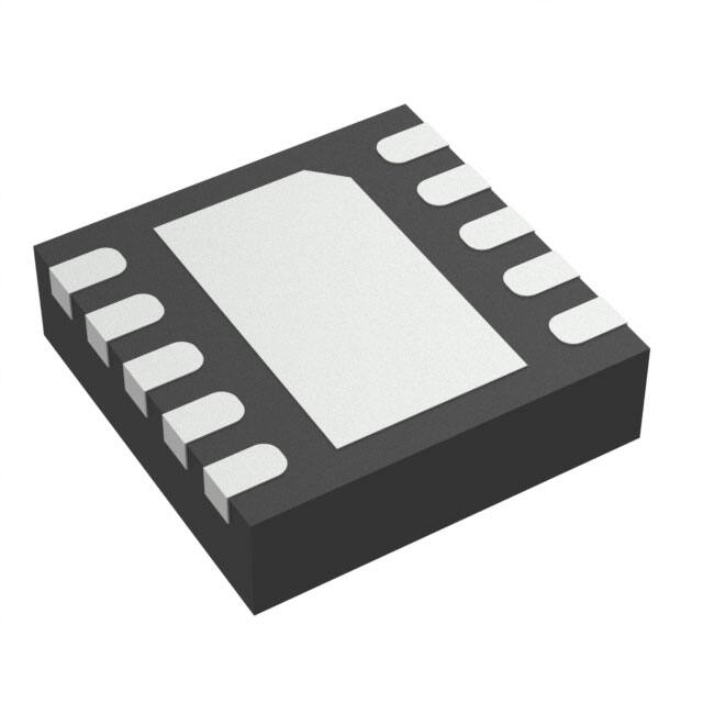
DRC 10
VSON - 1 mm max height
PLASTIC SMALL OUTLINE - NO LEAD
3 x 3, 0.5 mm pitch
This image is a representation of the package family, actual package may vary.
Refer to the product data sheet for package details.
4226193/A
www.ti.com
�PACKAGE OUTLINE
DRC0010J
VSON - 1 mm max height
SCALE 4.000
PLASTIC SMALL OUTLINE - NO LEAD
3.1
2.9
A
B
PIN 1 INDEX AREA
3.1
2.9
1.0
0.8
C
SEATING PLANE
0.05
0.00
0.08 C
1.65 0.1
2X (0.5)
EXPOSED
THERMAL PAD
(0.2) TYP
4X (0.25)
5
2X
2
6
11
SYMM
2.4 0.1
10
1
8X 0.5
PIN 1 ID
(OPTIONAL)
10X
SYMM
0.5
10X
0.3
0.30
0.18
0.1
0.05
C A B
C
4218878/B 07/2018
NOTES:
1. All linear dimensions are in millimeters. Any dimensions in parenthesis are for reference only. Dimensioning and tolerancing
per ASME Y14.5M.
2. This drawing is subject to change without notice.
3. The package thermal pad must be soldered to the printed circuit board for optimal thermal and mechanical performance.
www.ti.com
�EXAMPLE BOARD LAYOUT
DRC0010J
VSON - 1 mm max height
PLASTIC SMALL OUTLINE - NO LEAD
(1.65)
(0.5)
10X (0.6)
1
10
10X (0.24)
11
(2.4)
SYMM
(3.4)
(0.95)
8X (0.5)
6
5
(R0.05) TYP
( 0.2) VIA
TYP
(0.25)
(0.575)
SYMM
(2.8)
LAND PATTERN EXAMPLE
EXPOSED METAL SHOWN
SCALE:20X
0.07 MAX
ALL AROUND
0.07 MIN
ALL AROUND
EXPOSED METAL
EXPOSED METAL
SOLDER MASK
OPENING
METAL
METAL UNDER
SOLDER MASK
NON SOLDER MASK
DEFINED
(PREFERRED)
SOLDER MASK
OPENING
SOLDER MASK
DEFINED
SOLDER MASK DETAILS
4218878/B 07/2018
NOTES: (continued)
4. This package is designed to be soldered to a thermal pad on the board. For more information, see Texas Instruments literature
number SLUA271 (www.ti.com/lit/slua271).
5. Vias are optional depending on application, refer to device data sheet. If any vias are implemented, refer to their locations shown
on this view. It is recommended that vias under paste be filled, plugged or tented.
www.ti.com
�EXAMPLE STENCIL DESIGN
DRC0010J
VSON - 1 mm max height
PLASTIC SMALL OUTLINE - NO LEAD
2X (1.5)
(0.5)
SYMM
EXPOSED METAL
TYP
11
10X (0.6)
1
10
(1.53)
10X (0.24)
2X
(1.06)
SYMM
(0.63)
8X (0.5)
6
5
(R0.05) TYP
4X (0.34)
4X (0.25)
(2.8)
SOLDER PASTE EXAMPLE
BASED ON 0.125 mm THICK STENCIL
EXPOSED PAD 11:
80% PRINTED SOLDER COVERAGE BY AREA
SCALE:25X
4218878/B 07/2018
NOTES: (continued)
6. Laser cutting apertures with trapezoidal walls and rounded corners may offer better paste release. IPC-7525 may have alternate
design recommendations.
www.ti.com
�IMPORTANT NOTICE AND DISCLAIMER
TI PROVIDES TECHNICAL AND RELIABILITY DATA (INCLUDING DATA SHEETS), DESIGN RESOURCES (INCLUDING REFERENCE
DESIGNS), APPLICATION OR OTHER DESIGN ADVICE, WEB TOOLS, SAFETY INFORMATION, AND OTHER RESOURCES “AS IS”
AND WITH ALL FAULTS, AND DISCLAIMS ALL WARRANTIES, EXPRESS AND IMPLIED, INCLUDING WITHOUT LIMITATION ANY
IMPLIED WARRANTIES OF MERCHANTABILITY, FITNESS FOR A PARTICULAR PURPOSE OR NON-INFRINGEMENT OF THIRD
PARTY INTELLECTUAL PROPERTY RIGHTS.
These resources are intended for skilled developers designing with TI products. You are solely responsible for (1) selecting the appropriate
TI products for your application, (2) designing, validating and testing your application, and (3) ensuring your application meets applicable
standards, and any other safety, security, regulatory or other requirements.
These resources are subject to change without notice. TI grants you permission to use these resources only for development of an
application that uses the TI products described in the resource. Other reproduction and display of these resources is prohibited. No license
is granted to any other TI intellectual property right or to any third party intellectual property right. TI disclaims responsibility for, and you
will fully indemnify TI and its representatives against, any claims, damages, costs, losses, and liabilities arising out of your use of these
resources.
TI’s products are provided subject to TI’s Terms of Sale or other applicable terms available either on ti.com or provided in conjunction with
such TI products. TI’s provision of these resources does not expand or otherwise alter TI’s applicable warranties or warranty disclaimers for
TI products.
TI objects to and rejects any additional or different terms you may have proposed. IMPORTANT NOTICE
Mailing Address: Texas Instruments, Post Office Box 655303, Dallas, Texas 75265
Copyright © 2022, Texas Instruments Incorporated
�


 工商网监
湘ICP备2023018690号
工商网监
湘ICP备2023018690号
