�������
�
�
�� �� ��
���
�� ������
�
� � �� ����� �
���
����
SLVS278E – AUGUST 2000 – REVISED MARCH 2003
D Independent Dual-Outputs Operate 180°
D
D
D
D
D
D
D
D
D
D
D
D
Out of Phase
Wide Input Voltage Range: 4.5-V – 28-V
Adjustable Output Voltage Down to 0.9 V
Pin-Selectable PWM/SKIP Mode for High
Efficiency Under Light Loads
Synchronous Buck Operation Allows up to
95% Efficiency
Separate Standby Control and Overcurrent
Protection for Each Channel
Programmable Short-Circuit Protection
Low Supply (1 mA) and Shutdown (1 nA)
Current
Power Good Output
High-Speed Error Amplifiers
Sequencing Easily Achieved by Selecting
Softstart Capacitor Values.
5-V Linear Regulator Power Internal IC
Circuitry
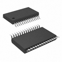
30-Pin TSSOP Packaging
DBT PACKAGE
(TOP VIEW)
INV1
FB1
SOFTSTART1
PWM/SKIP
CT
5V_STBY
GND
REF
STBY1
STBY2
FLT
POWERGOOD
SOFTSTART2
FB2
INV2
1
2
3
4
5
6
7
8
9
10
11
12
13
14
15
30
29
28
27
26
25
24
23
22
21
20
19
18
17
16
LH1
OUT1_u
LL1
OUT1_d
OUTGND1
TRIP1
VCC
TRIP2
VREF5
REG5V_IN
OUTGND2
OUT2_d
LL2
OUT2_u
LH2
description
The TPS5120 is a dual channel, high-efficiency synchronous buck controller where the outputs run 180 degrees
out of phase, which lowers the input current ripple, thereby reducing the input capacitance cost. The PWM/SKIP
pin allows the operating mode to switch from PWM mode to skip mode under light load conditions. The skip
mode enables a lower operating frequency and shortens the pulse width to the low-side MOSFET, increasing
the efficiency under light load conditions. These two modes, along with synchronous-rectifier drivers, dead time,
and very low quiescent current, allow power to be conserved and the battery life to be extended under all load
conditions. The 1.5 A (typical) high-side and low-side MOSFET drivers on-chip are designed to drive less
expensive N-channel MOSFETs. The resistorless current protection and fixed high-side driver voltage simplify
the power supply design and reduce the external parts count. Each channel is independent, offering a separate
controller, overcurrent protection, and standby control. Sequencing is flexible and can be tailored by choosing
different softstart capacitor values. Other features, such as undervoltage lockout, power good, overvoltage,
undervoltage, and programmable short-circuit protection promote system reliability.
Please be aware that an important notice concerning availability, standard warranty, and use in critical applications of
Texas Instruments semiconductor products and disclaimers thereto appears at the end of this data sheet.
Copyright 2002, Texas Instruments Incorporated
��
� ���
� �
�
����� !"��� �# $%��&�" !# �� '%()�$!"��� *!"&+
���*%$"# $����� "� #'&$���$!"���# '&� ",& "&� # �� �&-!# ��#"�% &�"#
#"!�*!�* .!��!�"/+ ���*%$"��� '��$&##��0 *�&# ��" �&$&##!��)/ ��$)%*&
"&#"��0 �� !)) '!�! &"&�#+
POST OFFICE BOX 655303
• DALLAS, TEXAS 75265
1
��������
�
�
�� �� ��
���
�� ������
�
� � �� ����� �
���
����
SLVS278E – AUGUST 2000 – REVISED MARCH 2003
typical design
VI
C1
R1
R2
Q1
U1
TPS5120DBT
R3
GND
C3
1
2
C4
3
4
C5
5
6
7
C6
8
9
10
C7
11
12
C8
13
14
15
R4
LH1
INV1
FB1
OUT1_u
LL1
SOFTSTART1
PWM/SKIP
CT
5V_STBY
R7
OUT1_d
OUTGND1
TRIP1
GND
Vcc
REF
TRIP2
STBY1
VREF5
STBY2
REG5V_IN
FLT
OUTGND2
POWERGOOD
OUT2_d
LL2
SOFTSTART2
FB2
OUT2_u
INV2
LH2
L1
D1
30
29
28
C13
27
26
VO1
Q2
C11
C15
25
R8
R9
24
23
22
21
C16
20
19
18
17
C12
C14
D2
Q3
16
VO2
R10
L2
C10
C15
R5
R6
Figure 1. EVM Typical Design
2
POST OFFICE BOX 655303
• DALLAS, TEXAS 75265
Q4
��������
�
�
�� �� ��
���
�� ������
�
� � �� ����� �
���
����
SLVS278E – AUGUST 2000 – REVISED MARCH 2003
functional block diagram
SOFTSTART1
SOFTSTART1
PWM Comp.
LH1
Skip Comp.
_
_
+
DLY
OUT1_u
+
LL1
DLY
OUT1_d
FB1
_
+
+
INV1
OUTGND1
_
Err Amp.
+
0.85 V
–(V
CT
CC
_
FLT
OVP1
UVLO
SIGNAL
+
Current
Protection
Trigger
STBY1
0.85 V+12%
_
– VTRIP1)
+
_
OSC
LSD Trip
HSD Trip
TRIP1
Current Comp.
V
CC
– VTRIP1
OVP2
STBY2
+
V
CC
0.85 V+12%
V
UVP1
+
_
CC
– VTRIP2
_
Timer
0.85 V –19.4%
UVP2
+
_
TRIP2
+
Phase
Inverter
HSD Trip
_
0.85 V –19.4%
LSD Trip
FB2
–(V
_
+
+
INV2
CC
+
– VTRIP2)
OUTGND2
Err Amp.
OUT2_d
DLY
PWM Comp.
PWM/SKIP
_
+
LL2
_
OUT2_u
DLY
+
Skip Comp.
LH2
UVLO
SIGNAL
0.85 V
SOFTSTART2
_
SOFTSTART2
SFT1
SFT2
UVLO
Comp.
VCC
V
+
5.0 V
_
5 VREG
ref
STBY1
_
INV1
+
STBY2
REF
0.85 V
VREF5
REG5V_IN
+
4.5 V
PGcomp1
0.85 V–7%
POWERGOOD
5V_STBY
INV2
GND
+
_
INV1
PGcomp4
0.85 V +7%
+
_
INV2
PGcomp3
_
+
0.85 V +7%
PGcomp2
0.85 V –7%
POST OFFICE BOX 655303
• DALLAS, TEXAS 75265
3
��������
�
�
�� �� ��
���
�� ������
�
� � �� ����� �
���
����
SLVS278E – AUGUST 2000 – REVISED MARCH 2003
AVAILABLE OPTIONS
PACKAGE
TA
EVM
TSSOP
(DBT)
TPS5120DBT
–40°C
40°C to 85°C
TPS5120EVM-151
TPS5120DBTR
Terminal Functions
TERMINAL
NAME
CT
NO.
I/O
DESCRIPTION
5
I/O
External capacitor from CT to GND for adjusting the triangle oscillator
FB1
2
O
Feedback output of CH1 error amplifier
FB2
14
O
Feedback output of CH2 error amplifier
GND
7
INV1
1
I
Inverting input of the CH1 error amplifier, skip comparator, and OVP1/UVP1 comparator
INV2
15
I
Inverting input of the CH2 error amplifier, skip comparator, and OVP2/UVP2 comparator
LH1
30
I/O
Bootstrap capacitor connection for CH1 high-side gate drive
LH2
16
I/O
Bootstrap capacitor connection for CH2 high-side gate drive
LL1
28
I/O
Bootstrap this pin low for CH1 high-side gate driving return and output current protection. Connect this pin to
the junction of the high-side and low-side FETs for a floating drive configuration.
LL2
18
I/O
Bootstrap this pin low for CH2 high-side gate driving return and output current protection. Connect this pin to
the junction of the high-side and low-side FETs for a floating drive configuration.
OUT1_d
27
O
Gate drive output for CH1 low-side gate drive
OUT2_d
19
O
Gate drive output for CH2 low-side gate drive
OUT1_u
29
O
Gate drive output for CH1 high-side switching FETs
OUT2_u
17
O
Gate drive output for CH2 high-side switching FETs
OUTGND1
26
OUTGND2
20
POWERGOOD
12
O
Power good open-drain output. When low, POWERGOOD reports an output fail condition. PG comparators
monitor both SMPS’s over voltage and UVLO of VREF5. The threshold is ±7%. When the SMPS starts up, the
POWERGOOD pin’s output goes high. POWERGOOD also monitors VREF5’s UVLO output.
PWM/SKIP
4
I
PWM/SKIP mode select pin. The PWM/SKIP pin is used to change the output’s operating mode. If this terminal
is lower than 0.5 V, it works in PWM mode. When a minimum voltage of 2 V is applied, the device operates in
skip mode. In light load condition (< 0.2 A), the skip mode gives a short pulse to the low-side FETs instead of a
full pulse. With this control, switching frequency is lowered and switching loss is reduced. Also, the output
capacitor energy discharging through the output inductor and low-side FETs is stopped. Therefore, TPS5120
achieves a higher efficiency in light load conditions.
REF
8
O
0.85-V reference voltage output. The 0.85-V reference voltage is used for setting the output voltage and the
voltage protection. This reference voltage is dropped down from a 5-V regulator.
REG5V_IN
21
I
External 5-V input
FLT
11
I/O
Fault latch timer pin. An external capacitor is connected between FLT and GND to set the FLT enable time up.
SOFTSTART1
3
I/O
External capacitor from SOFTSTART1 to GND for CH1 softstart control. Separate soft-start terminals make it
possible to set the start-up time of each output independently.
SOFTSTART2
13
I/O
External capacitor from SOFTSTART2 to GND for CH2 softstart control. Separate soft-start terminals make it
possible to set the start-up time of each output independently.
STBY1
9
I
Standby control for CH1. SMPS1 can be switched into standby mode separately by grounding the STBY1 pin.
STBY2
10
I
Standby control for CH2. SMPS2 can be switched into standby mode separately by grounding the STBY2 pin.
TRIP1
25
I
External resistor connection for CH1 output current control
4
Control GND
Ground for CH1 FET drivers
Ground for CH2 FET drivers
POST OFFICE BOX 655303
• DALLAS, TEXAS 75265
��������
�
�
�� �� ��
���
�� ������
�
� � �� ����� �
���
����
SLVS278E – AUGUST 2000 – REVISED MARCH 2003
Terminal Functions (Continued)
TERMINAL
NAME
NO.
I/O
I
DESCRIPTION
TRIP2
23
External resistor connection for CH2 output current control
VCC
VREF5
24
22
O
5-V internal regulator output
5V_STBY
6
I
5-V linear regulator control
Supply voltage input
detailed description
switching-mode power supply (SMPS) 1, 2
TPS5120 includes dual SMPS controllers that operate 180° out of phase and at the same frequency. Both
channels have standby and softstart.
5-V regulator
An internal linear voltage regulator is used for the high-side driver bootstrap voltage and source of VREF
(0.85 V). When the 5-V regulator is disconnected from the MOSFET drivers, it is only used for the source of
VREF. Since the input voltage range is from 4.5 V to 28 V, this feature offers a fixed voltage for the bootstrap
voltage so that the drive design is much easier. It is also used for powering the low-side driver. The tolerance
is 4%. The 5-V regulator is disabled when STBY1, STBY2, and 5V_STBY are all set low.
5-V switch
If the internal 5-V switch senses the 5-V input from the REG5V_IN pin, the internal 5-V linear regulator is
disconnected from the MOSFET drivers. The external 5 V is then used for both the low-side driver and the
high-side bootstrap, thus, increasing the efficiency.
error amplifier
Each channel has its own error amplifier to regulate the output voltage of the synchronous buck converter. It
is used in the PWM mode for the high output current condition (> 0.2 A). The unity gain bandwidth is 2.5 MHz.
This decreases the amplifier delay during fast load transients and contributes to a fast transient response.
skip comparator
In skip mode, each channel has its own hysteretic comparator to regulate the output voltage of the synchronous
buck converter. The hysteresis is set internally and is typically set at 9 mV. The delay from the comparator input
to the driver output is typically 1.2 µs.
low-side driver
The low-side driver is designed to drive low rds(on) N-channel MOSFETs. The maximum drive voltage is 5 V from
VREF5. The current rating of the driver is typically 1.5 A at source and sink.
high-side driver
The high-side driver is designed to drive low rds(on) N-channel MOSFETs. The current rating of the driver is 1.2 A
at source and sink. When configured as a floating driver, the bias voltage to the driver is developed from VREF5,
limiting the maximum drive voltage between OUTx_u and LLx to 5 V. The maximum voltage that can be applied
between LHx and OUTGND is 33 V.
deadtime
Deadtime prevents shoot through current from flowing through the main power FETs during switching transitions
by actively controlling the turnon time of the MOSFETs drivers.
POST OFFICE BOX 655303
• DALLAS, TEXAS 75265
5
��������
�
�
�� �� ��
���
�� ������
�
� � �� ����� �
���
����
SLVS278E – AUGUST 2000 – REVISED MARCH 2003
detailed description (continued)
current protection
Overcurrent protection is achieved by comparing the drain-to-source voltage of the high-side and low-side
MOSFET devices to a set-point voltage. This voltage is set using an external resistor between VCC and the
TRIP1 or TRIP2 terminals. If the drain-to-source voltage up exceeds the set-point voltage during high-side
conduction, the current limit circuit terminates the high-side driver pulse. If the set-point voltage is exceeded
during low-side conduction, the low-side pulse is extended through the next cycle. Together this action has the
effect of decreasing the output voltage until the undervoltage protection circuit is activated and the fault latch
is set and both the high and low-side MOSFET drivers are shut off.
overvoltage protection
For overvoltage protection (OVP), the TPS5120 monitors INV pin voltage. When the INV voltage is higher than
0.95 V (+12%), the OVP comparator output goes high and the FLT timer starts to charge an external capacitor
connected to FLT. After a set time, the FLT circuit latches the MOSFET drivers off.
undervoltage protection
For undervoltage protection (UVP), the TPS5120 monitors INV pin voltage. When the INV voltage is lower than
0.68 V (–19.4%), the OVP comparator output goes high, and the FLT timer starts to charge an external capacitor
connected to FLT. Also, when the current comparator triggers the OCP, the UVP comparator detects the under
voltage output and starts the FLT capacitor charge. After a set time, the FLT circuit latches off all of the MOSFET
drivers.
FLT
When an OVP or UVP comparator output goes high, the FLT circuit starts to charge the FLT capacitor. If the
FLT pin voltage goes beyond a constant level, the TPS5120 latches the MOSFET drivers. At this time, the state
of MOSFET is different depending on the OVP alert and the UVP alert. Also, the enable time used to latch the
MOSFET driver is decided by the capacity of the FLT capacitor. The charging constant current value is also
different depending on whether it is an OVP alert or a UVP alert. The difference is shown in the following
equation:
FLT source current (OVP) = FLT source current (UVP) × 5
shutdown
The TPS5120 can be shut down by grounding STBY1, STBY2, and 5V_STBY. The shutdown current is as low
as 1 µA.
UVLO
When the input voltage goes up to about 4 V, the TPS5120 is operational. When the input voltage is lower than
the turnon value, the device is turned off. The typical hysteresis voltage is 40 mV.
phase Inverter
Phase inverter controls the phase of SMPS1 and SMPS 2. SMPS1 operates in phase with the OSC. SMPS2
operates 180° out of phase from SMPS1. This allows smaller input capacitors to be used.
oscillator
TPS5120 has a triangle oscillator generator internal to the IC. The oscillation frequency is set by the size of the
capacitor connected to the CT pin. The voltage amplitude is 0.43 V ~ 1.17 V.
6
POST OFFICE BOX 655303
• DALLAS, TEXAS 75265
��������
�
�
�� �� ��
���
�� ������
�
� � �� ����� �
���
����
SLVS278E – AUGUST 2000 – REVISED MARCH 2003
Table 1. Logic Chart
5V_STBY
STBY1
STBY2
SMPS1
SMPS2
5 V REGULATOR
POWERGOOD
L
L
L
L
Disable
Disable
Disable
L
H
Disable
Enable
Enable
Disable
Active†
L
H
L
Enable
Disable
Enable
Active†
L
H
H
Enable
Enable
Enable
Active
H
L
L
Disable
Disable
Enable
L
H
L
H
Disable
Enable
Enable
H
H
L
Enable
Disable
Enable
Active†
Active†
H
Enable
Enable
Enable
Active
H
H
† PG is set high during a softstart.
POWERGOOD timing sequence
TSS
H
POWERGOOD
L
H
STBY1
L
H
STBY2
L
0.91 V
0.85 V
0.78 V
INV1
0V
0.91 V
INV2
0.85 V
0.78 V
0V
During a softstart, this channel’s powergood comparator output is fixed low (POWERGOOD output is high).
POST OFFICE BOX 655303
• DALLAS, TEXAS 75265
7
��������
�
�
�� �� ��
���
�� ������
�
� � �� ����� �
���
����
SLVS278E – AUGUST 2000 – REVISED MARCH 2003
absolute maximum ratings over operating free-air temperature (unless otherwise noted)†
Supply voltage, VCC (see Note 1) . . . . . . . . . . . . . . . . . . . . . . . . . . . . . . . . . . . . . . . . . . . . . . . . . . . –0.3 V to 30 V
Input voltage: INV1, INV2, CT, PWM/SKIP, REG5V_IN, SOFTSTART1, SOFTSTART2, . . . . . –0.3 V to 7 V
FLT, POWERGOOD . . . . . . . . . . . . . . . . . . . . . . . . . . . . . . . . . . . . . . . . . . . . . . . . . . –0.3 V to 7 V
STBY1, STBY2, 5V_STBY, TRIP1, TRIP2 . . . . . . . . . . . . . . . . . . . . . . . . . . . . . . –0.3 V to 30 V
Output voltage: LL1, LL2 . . . . . . . . . . . . . . . . . . . . . . . . . . . . . . . . . . . . . . . . . . . . . . . . . . . . . . . . . –1.0 V to 30 V
OUT1_u, OUT2_u . . . . . . . . . . . . . . . . . . . . . . . . . . . . . . . . . . . . . . . . . . . . . . . . . –1.0 V to 35 V
LH1, LH2 . . . . . . . . . . . . . . . . . . . . . . . . . . . . . . . . . . . . . . . . . . . . . . . . . . . . . . . . . –0.3 V to 35 V
OUT1_d, OUT2_d, 5V_OUT, FB1, FB2 . . . . . . . . . . . . . . . . . . . . . . . . . . . . . . . . –0.3 V to 7 V
REF . . . . . . . . . . . . . . . . . . . . . . . . . . . . . . . . . . . . . . . . . . . . . . . . . . . . . . . . . . . . . . –0.3 V to 3 V
OUT1_u, LH1 to LL1 . . . . . . . . . . . . . . . . . . . . . . . . . . . . . . . . . . . . . . . . . . . . . . . . –0.3 V to 7 V
OUT2_u, LH2 to LL2 . . . . . . . . . . . . . . . . . . . . . . . . . . . . . . . . . . . . . . . . . . . . . . . . –0.3 V to 7 V
Power dissipation (TA ≤ 25°C), PD . . . . . . . . . . . . . . . . . . . . . . . . . . . . . . . . . . . . . . . . . . . . . . . . . . . . . . . . 874 mW
Operating free-air temperature range, TA . . . . . . . . . . . . . . . . . . . . . . . . . . . . . . . . . . . . . . . . . . . . –40°C to 85°C
Storage temperature range, Tstg . . . . . . . . . . . . . . . . . . . . . . . . . . . . . . . . . . . . . . . . . . . . . . . . . . . –55°C to 150°C
† Stresses beyond those listed under “absolute maximum ratings” may cause permanent damage to the device. These are stress ratings only, and
functional operation of the device at these or any other conditions beyond those indicated under “recommended operating conditions” is not
implied. Exposure to absolute-maximum-rated conditions for extended periods may affect device reliability.
NOTES: 1. All voltage values are with respect to the network ground terminal unless otherwise noted.
2. This rating is specified at duty = 10% on output rise and fall each pulse. Each pulse width (rise and fall) for the peak current should
not exceed 2 µs.
3. See Dissipation Rating Table for free-air temperature range above 25°C.
DISSIPATION RATING TABLE
PACKAGE
TA ≤ 25°C
POWER RATING
DBT
874 mW
DERATING FACTOR
ABOVE TA = 25°C
6.993 mW/°C
POWER DISSIPATION
TA = 85°C
454 mW
recommended operating conditions
MIN
Supply voltage, VCC
NOM
28
–0.1
5.5
INV1, INV2, CT, PWM/SKIP, SOFTSTART1, SOFTSTART2, FLT
REG5V_IN, POWERGOOD
Input
In
ut voltage, VI
STBY1, STBY2, 5V_STBY
28
OUT1_u, OUT2_u, LH1, LH2
33
TRIP1, TRIP2
–0.1
–40
POST OFFICE BOX 655303
• DALLAS, TEXAS 75265
V
V
28
300
Operating free-air temperature range, TA
UNIT
6
Oscillator frequency, fosc
8
MAX
4.5
500
kHz
85
°C
��������
�
�
�� �� ��
���
�� ������
�
� � �� ����� �
���
����
SLVS278E – AUGUST 2000 – REVISED MARCH 2003
electrical characteristics over recommended free-air temperature range, VCC = 7 V (unless
otherwise noted)
reference voltage
PARAMETER
Vref
TEST CONDITIONS
MIN
Reference voltage
TYP
MAX
0.85
V
I = 50 µA
–1%
1%
Reference voltage tolerance
TA = 25°C,
TA = –20°C to 85°C,
I = 50 µA
–1.5%
1.5%
I = 50 µA
–2%
R(egin)
Line regulation
TA = –40°C to 85°C,
VCC = 4.5 V to 28 V,
R(egl)
Load regulation
I = 0.1 µA to 1 mA
Vref(tol)
I = 50 µA
UNIT
2%
0.05
3
mV
0.15
5
mV
TYP
MAX
oscillator
PARAMETER
fosc
Frequency
TEST CONDITIONS
PWM mode,
DC
VOH
High le
level
el o
output
tp t voltage
oltage
VOL
Lo le
Low
level
el o
output
tp t voltage
oltage
MIN
TA = 25 °C
CT = 44 pF,
300
1
fosc = 300 kHz
DC
1.1
kHz
1.2
V
1.17
0.4
fosc = 300 kHz
0.5
UNIT
0.6
V
0.43
error amplifier
PARAMETER
VIO
TEST CONDITIONS
Input offset voltage
MIN
TA = 25°C
Open-loop voltage gain
MAX
2
10
50
Unity-gain bandwidth
I(snk)
I(src)
TYP
Output sink current
VO = 1 V
VO = 1 V
Output source current
UNIT
mV
dB
2.5
MHz
0.3
0.7
mA
0.2
0.9
mA
MIN
TYP
skip comparator
PARAMETER
Vhys
TEST CONDITIONS
Hysteresis window
SKIP mode
MAX
9
UNIT
mV
duty control
PARAMETER
DUTY
TEST CONDITIONS
Maximum duty cycle
300 kHz,
MIN
VI = 0 V
TYP
MAX
UNIT
MAX
UNIT
83%
control
PARAMETER
VIH
High le el inp
High-level
inputt voltage
oltage
VIL
Lo le el inp
Low-level
inputt voltage
oltage
TEST CONDITIONS
MIN
STBY1, STBY2
2.2
PWM/SKIP, 5V_STBY
2.2
TYP
V
STBY1, STBY2
0.3
PWM/SKIP, 5V_STBY
0.3
V
5-V internal switch
PARAMETER
V(TO_H)
V(TO_L)
Threshold
Vhys
Hysteresis
TEST CONDITIONS
POST OFFICE BOX 655303
• DALLAS, TEXAS 75265
MIN
TYP
MAX
4.2
4.8
4.1
4.7
30
200
UNIT
V
mV
9
��������
�
�
�� �� ��
���
�� ������
�
� � �� ����� �
���
����
SLVS278E – AUGUST 2000 – REVISED MARCH 2003
electrical characteristics over recommended free-air temperature range, VCC = 7 V (unless
otherwise noted) (continued)
5-V regulator
PARAMETER
IO = 0 mA to 50 mA,
TA = 25°C
VCC = 5.5 V to 28 V,
Load regulation
VCC = 5.5 V to 28 V,
I = 1 mA to 10 mA,
Short circuit output current
5VREG = 0 V,
VO
Output voltage
R(egin)
Line regulation
R(egl)
IOS
V(TO_H)
V(TO_L)
Vhys
TEST CONDITIONS
UVLO threshold voltage
5V OUT voltage
5V_OUT
Hysteresis
5V_OUT voltage
MIN
TYP
4.8
MAX
UNIT
5.2
V
I =10 mA
20
mV
VCC = 5.5 V
TA = 25°C
40
mV
65
mA
3.6
4.2
3.5
4.1
30
150
mV
MAX
UNIT
V
output drivers
PARAMETER
TEST CONDITIONS
OUT_u sink current
VO = 3 V
VO = 2 V
OUT_u source current
OUT_d sink current
I(TRIP)
MIN
TYP
1.2
A
–1.5
A
1.5
A
OUT_d source current
VO = 3 V
VO = 2 V
TRIP pin current
TA = 25°C
11.5
13
14.5
µA
TEST CONDITIONS
MIN
TYP
MAX
UNIT
1.6
2.3
2.9
–1.5
A
soft start
PARAMETER
I(SOFT)
V(TO_H)
V(TO_L)
Soft start current
µA
3.7
Threshold voltage (SKIP mode)
V
2.5
output voltage monitor
PARAMETER
TEST CONDITIONS
MIN
TYP
MAX
UNIT
OVP comparator threshold
0.91
0.95
0.99
V
UVP comparator threshold
0.64
0.68
0.72
V
PG comparator 1, 2 threshold
0.75
0.78
0.81
V
0.88
0.91
0.94
V
PG comparator 3, 4 threshold
PG propagation delay
dela from INV to POWERGOOD
Timer latch current source
Turnon
13
Turnoff
1.2
µss
UVP protection
1.5
2.3
3.1
OVP protection
8
11.5
15
MIN
TYP
MAX
1.1
1.5
mA
0.001
10
µA
A
µA
supply current
PARAMETER
ICC
ICC(S)
10
Supply current
Shutdown current
TEST CONDITIONS
TA = 25°C, CT = 0 V, INV = 0 V
STBY 1, STBY2, 5V_STBY = 0 V
POST OFFICE BOX 655303
• DALLAS, TEXAS 75265
UNIT
��������
�
�
�� �� ��
���
�� ������
�
� � �� ����� �
���
����
SLVS278E – AUGUST 2000 – REVISED MARCH 2003
TYPICAL CHARACTERISTICS
QUIESCENT CURRENT
vs
JUNCTION TEMPERATURE
QUIESCENT CURRENT (SHUTDOWN)
vs
JUNCTION TEMPERATURE
1200
1.25
VCC = 28 V
Icc(s) – Quiescent Current – nA
Icc – Quiescent Current – mA
1.30
1.20
1.15
1.10
VCC = 4.5 V
VCC = 7 V
1.05
–50
0
50
100
TJ – Junction Temperature – °C
1000
VCC = 28 V
800
VCC = 7 V
600
400
VCC = 4.5 V
200
0
–50
150
0
50
100
TJ – Junction Temperature – °C
Figure 2
Figure 3
DRIVE OUTPUT CURRENT (OUT_u)
vs
DRIVE OUTPUT VOLTAGE
DRIVE OUTPUT CURRENT (OUT_u)
vs
DRIVE OUTPUT VOLTAGE
1.50
I O(SINK) – Drive Output Current (OUT_u) – A
I O(SOURCE)– Drive Output Current (OUT_u) – A
–1.80
TJ = –40 °C
–1.70
–1.60
–1.50
–1.40
–1.30
TJ = 25 °C
–1.20
TJ = 85 °C
–1.10
TJ = 125 °C
–1.00
–0.90
–0.80
0.5
150
TJ = –20 °C
1
1.5
2
2.5
3
3.5
VO – Drive Output Voltage (OUT_u) – V
1.40
TJ = –40 °C
1.30
1.20
1.10
1.00
0.90
TJ = 85 °C
0.80
0.70
0.60
1.5
TJ = –20 °C
TJ = 25 °C
TJ = 125 °C
2.5
3.5
2
3
4
VO – Drive Output Voltage (OUT_u) – V
Figure 4
4.5
Figure 5
POST OFFICE BOX 655303
• DALLAS, TEXAS 75265
11
��������
�
�
�� �� ��
���
�� ������
�
� � �� ����� �
���
����
SLVS278E – AUGUST 2000 – REVISED MARCH 2003
TYPICAL CHARACTERISTICS
DRIVE OUTPUT CURRENT (OUT_d)
vs
DRIVE OUTPUT VOLTAGE
1.80
–2.00
TJ = –40 °C
I O(SINK) – Drive Output Current (OUT_d) – A
I O(SOURCE) – Drive Output Current (OUT_d) – A
DRIVE OUTPUT CURRENT (OUT_d)
vs
DRIVE OUTPUT VOLTAGE
TJ = –20 °C
–1.80
TJ = 25 °C
–1.60
–1.40
–1.20
–1.00
–0.80
0.5
TJ = 85 °C
TJ = 125 °C
1.5
2.5
2
3
VO – Drive Output Voltage (OUT_d) – V
1
1.70
TJ = –40 °C
1.60
1.50
1.40
1.30
1.20
1.00
2.5
3
3.5
4
4.5
Figure 7
OSCILLATOR OUTPUT VOLTAGE
vs
JUNCTION TEMPERATURE
1.20
500
V(OSCL) – Oscillator Output Voltage – mV
V
– Oscillator Output Voltage – V
(OSCH)
2
TJ = 125 °C
VO – Drive Output Voltage (OUT_d) – V
OSCILLATOR OUTPUT VOLTAGE
vs
JUNCTION TEMPERATURE
1.18
1.16
1.14
1.12
1.10
1.08
VCC = 4.5 V,
VCC = 7 V,
VCC = 28 V
1.06
1.04
1.02
0
50
100
TJ – Junction Temperature – °C
150
VCC = 4.5 V,
VCC = 7 V,
VCC = 28 V
495
490
485
480
–50
Figure 8
12
TJ = 25 °C
0.90
Figure 6
1.00
–50
TJ = 85 °C
1.10
0.80
1.5
3.5
TJ = –20 °C
0
50
100
TJ – Junction Temperature – °C
Figure 9
POST OFFICE BOX 655303
• DALLAS, TEXAS 75265
150
��������
�
�
�� �� ��
���
�� ������
�
� � �� ����� �
���
����
SLVS278E – AUGUST 2000 – REVISED MARCH 2003
TYPICAL CHARACTERISTICS
ERROR AMPLIFIER OUTPUT VOLTAGE
vs
JUNCTION TEMPERATURE
ERROR AMPLIFIER INPUT OFFSET VOLTAGE
vs
JUNCTION TEMPERATURE
VO+ – Positive Error Amplifier Output Voltage – V
V IO – Error Amplifier Input Offset Voltage – mV
2.55
2.50
VCC = 28 V
2.45
2.40
2.35
2.30
VCC = 4.5 V,
VCC = 7 V
2.25
2.20
–50
0
50
100
TJ – Junction Temperature – °C
150
3.00
VCC = 4.5 V,
VCC = 7 V,
VCC = 28 V
2.75
2.50
2.25
2.00
1.75
1.50
–50
0
50
100
TJ – Junction Temperature – °C
Figure 10
Figure 11
SKIP COMPARATOR HYSTERESIS VOLTAGE
vs
JUNCTION TEMPERATURE
8.0
V
– Skip Comparator Hysteresis Voltage – mV
hys
VO– – Negative Error Amplifier Output Voltage – mV
ERROR AMPLIFIER OUTPUT VOLTAGE
vs
JUNCTION TEMPERATURE
7.0
VCC = 4.5 V,
VCC = 7 V,
VCC = 28 V
6.0
5.0
4.0
3.0
2.0
1.0
0.0
–50
150
0
50
100
TJ – Junction Temperature – °C
150
9.0
8.8
VCC = 28 V
VCC = 7 V
8.6
8.4
8.2
8.0
7.8
7.6
VCC = 4.5 V
7.4
7.2
7.0
–50
Figure 12
0
50
100
TJ – Junction Temperature – °C
150
Figure 13
POST OFFICE BOX 655303
• DALLAS, TEXAS 75265
13
��������
�
�
�� �� ��
���
�� ������
�
� � �� ����� �
���
����
SLVS278E – AUGUST 2000 – REVISED MARCH 2003
TYPICAL CHARACTERISTICS
VREF5 SHORT-CIRCUIT OUTPUT CURRENT
vs
JUNCTION TEMPERATURE
VREF5 OUTPUT VOLTAGE
vs
OUTPUT CURRENT
–120
5.20
– VREF5 Short–Circuit Output Current – mA
OS
TJ = 125 °C
VO – VREF5 Output Voltage – V
5.10
5.00
4.90
TJ = 85 °C
4.80
4.70
TJ = 25 °C
4.60
TJ = –40 °C
–80
VCC = 28 V
–60
–40
–20
VCC = 7 V
VCC = 4.5 V
I
TJ = –20 °C
–100
4.50
0
–10
–20
–30
–40
–50
I O – Output Current – mA
0
–50
–60
UVLO HYSTERESIS VOLTAGE
vs
JUNCTION TEMPERATURE
UVLO THRESHOLD VOLTAGE
vs
JUNCTION TEMPERATURE
140
Vhys – UVLO Hysteresis Voltage – mV
V(TO) – UVLO Threshold Voltage – V
4.00
V(TO_H)
3.90
3.80
V(TO_L)
3.60
3.50
–50
120
100
80
60
40
20
0
0
50
100
TJ – Junction Temperature – °C
150
–50
Figure 16
14
150
Figure 15
Figure 14
3.70
0
50
100
TJ – Junction Temperature – °C
0
50
100
TJ – Junction Temperature – °C
Figure 17
POST OFFICE BOX 655303
• DALLAS, TEXAS 75265
150
��������
�
�
�� �� ��
���
�� ������
�
� � �� ����� �
���
����
SLVS278E – AUGUST 2000 – REVISED MARCH 2003
TYPICAL CHARACTERISTICS
REG5V_IN HYSTERESIS VOLTAGE
vs
JUNCTION TEMPERATURE
REG5V_IN THRESHOLD VOLTAGE
vs
JUNCTION TEMPERATURE
140
4.7
Vhys – REG5V_IN Hysteresis Voltage – mV
V(TO) – REG5V_IN Threshold Voltage – V
4.7
V(TO_L)
4.6
4.6
4.5
V(TO_H)
4.5
4.4
–50
0
50
100
TJ – Junction Temperature – °C
120
100
80
60
40
20
0
–50
150
Figure 18
OVP THRESHOLD VOLTAGE
vs
JUNCTION TEMPERATURE
–2.30
956
V(TO) – OVP Threshold Voltage – mV
–2.28
–2.26
Softstart Current – µA
150
Figure 19
SOFTSTART CURRENT
vs
JUNCTION TEMPERATURE
–2.24
VCC = 7 V,
VCC = 28 V
–2.22
–2.20
–2.18
–2.16
0
50
100
TJ – Junction Temperature – °C
VCC = 4.5 V
–2.14
954
VCC = 7 V,
VCC = 28 V
952
950
VCC = 4.5 V
948
946
–2.12
–2.10 –50
0
50
100
TJ – Junction Temperature – °C
150
944
–50
Figure 20
0
50
100
TJ – Junction Temperature – °C
150
Figure 21
POST OFFICE BOX 655303
• DALLAS, TEXAS 75265
15
��������
�
�
�� �� ��
���
�� ������
�
� � �� ����� �
���
����
SLVS278E – AUGUST 2000 – REVISED MARCH 2003
TYPICAL CHARACTERISTICS
SCP (OVP) SOURCE CURRENT
vs
JUNCTION TEMPERATURE
POWERGOOD THRESHOLD VOLTAGE
vs
JUNCTION TEMPERATURE
–12.0
900
875
–11.9
V(TO_H)
925
SCP (OVP) Source Current – µ A
V(TO) – Powergood Threshold Voltage – mV
950
VCC = 4.5 V,
VCC = 7 V,
VCC = 28 V
850
825
VCC = 4.5 V,
VCC = 7 V,
VCC = 28 V
800
775
750
–50
–11.8
VCC = 7 V,
VCC = 28 V
–11.7
–11.6
–11.5
–11.4
–11.3
VCC = 4.5 V
–11.2
–11.1
V(TO_L)
0
50
100
–11.0
–50
150
0
50
100
TJ – Junction Temperature – °C
TJ – Junction Temperature – °C
Figure 23
Figure 22
TRIP SINK CURRENT
vs
TRIP INPUT VOLTAGE
SCP (OVP) SOURCE CURRENT
vs
JUNCTION TEMPERATURE
14.0
13.8
VCC = 7 V,
VCC = 28 V
I(SINK) – TRIP Sink Current – µA
I
(SOURCE) – SCP (OVP) Source Current – µ A
–2.40
–2.38
–2.35
–2.33
–2.30
–2.28
VCC = 4.5 V
–2.25
–2.23
–2.20
–50
TJ = 125 °C
TJ = 85 °C
13.6
13.4
13.2
TJ = 25 °C
13.0
12.8
TJ = –20 °C
12.6
TJ = –40 °C
12.4
12.2
12.0
0
50
100
TJ – Junction Temperature – °C
150
0
4
8
12
16
Figure 25
POST OFFICE BOX 655303
20
24
VI – TRIP Input Voltage – V
Figure 24
16
150
• DALLAS, TEXAS 75265
28
32
��������
�
�
�� �� ��
���
�� ������
�
� � �� ����� �
���
����
SLVS278E – AUGUST 2000 – REVISED MARCH 2003
TYPICAL CHARACTERISTICS
OUTPUT MAXIMUM DUTY CYCLE
vs
JUNCTION TEMPERATURE
OSCILLATOR FREQUENCY
vs
CAPACITANCE
85.0
VCC = 7 V,
TJ = 25 °C
Output Maximum Duty Cycle – %
f OSC – Oscillator Frequency – kHz
1000
100
VCC = 7 V,
VCC = 28 V
84.5
84.0
83.5
83.0
VCC = 4.5 V
82.5
82.0
81.5
fosc = 300 kHz
10
0
81.0
50
100
150
200
CT – Capacitance – pF
–50
250
Figure 26
150
Figure 27
SOFTSTART TIME
vs
SOFTSTART CAPACITANCE
SCP DELAY TIME
vs
CAPACITANCE
100 k
100 k
10 k
10 k
t – Softstart Time – µs
td(SCP) – SCP Delay Time (OVP) –µ s
0
50
100
TJ – Junction Temperature – °C
1k
100
1k
100
10
1
10
100
1k
10 k
SCP – Capacitance – pF
100 k
10
100
1k
10 k
Softstart Capacitance – pF
100 k
Figure 29
Figure 28
POST OFFICE BOX 655303
• DALLAS, TEXAS 75265
17
��������
�
�
�� �� ��
���
�� ������
�
� � �� ����� �
���
����
SLVS278E – AUGUST 2000 – REVISED MARCH 2003
TYPICAL CHARACTERISTICS
DRIVER DEAD TIME (OUT_u FALL)
vs
JUNCTION TEMPERATURE
DRIVER DEAD RISE TIME (OUT_u RISE)
vs
JUNCTION TEMPERATURE
175.0
100
Driver and Dead Rise Time (OUT_u RISE)
VCC = 4.5 V
Driver Dead Time – ns
172.5
170.0
167.5
165.0
162.5
–50
VCC = 7 V,
VCC = 28 V
0
50
100
TJ – Junction Temperature – °C
150
95
90
VCC = 7 V,
VCC = 28 V
85
80
75
70
–50
Figure 30
18
VCC = 4.5 V
0
50
TJ – Junction Temperature – °C
Figure 31
POST OFFICE BOX 655303
• DALLAS, TEXAS 75265
100
�PACKAGE OPTION ADDENDUM
www.ti.com
13-Jul-2022
PACKAGING INFORMATION
Orderable Device
Status
(1)
Package Type Package Pins Package
Drawing
Qty
Eco Plan
(2)
Lead finish/
Ball material
MSL Peak Temp
Op Temp (°C)
Device Marking
(3)
Samples
(4/5)
(6)
TPS5120DBT
ACTIVE
TSSOP
DBT
30
60
RoHS & Green
NIPDAU
Level-2-260C-1 YEAR
-40 to 85
PS5120
Samples
TPS5120DBTR
ACTIVE
TSSOP
DBT
30
2000
RoHS & Green
NIPDAU
Level-2-260C-1 YEAR
-40 to 85
PS5120
Samples
TPS5120DBTRG4
ACTIVE
TSSOP
DBT
30
2000
RoHS & Green
NIPDAU
Level-2-260C-1 YEAR
-40 to 85
PS5120
Samples
(1)
The marketing status values are defined as follows:
ACTIVE: Product device recommended for new designs.
LIFEBUY: TI has announced that the device will be discontinued, and a lifetime-buy period is in effect.
NRND: Not recommended for new designs. Device is in production to support existing customers, but TI does not recommend using this part in a new design.
PREVIEW: Device has been announced but is not in production. Samples may or may not be available.
OBSOLETE: TI has discontinued the production of the device.
(2)
RoHS: TI defines "RoHS" to mean semiconductor products that are compliant with the current EU RoHS requirements for all 10 RoHS substances, including the requirement that RoHS substance
do not exceed 0.1% by weight in homogeneous materials. Where designed to be soldered at high temperatures, "RoHS" products are suitable for use in specified lead-free processes. TI may
reference these types of products as "Pb-Free".
RoHS Exempt: TI defines "RoHS Exempt" to mean products that contain lead but are compliant with EU RoHS pursuant to a specific EU RoHS exemption.
Green: TI defines "Green" to mean the content of Chlorine (Cl) and Bromine (Br) based flame retardants meet JS709B low halogen requirements of


 工商网监
湘ICP备2023018690号
工商网监
湘ICP备2023018690号
