TPS51312
www.ti.com
SLUSB57 – SEPTEMBER 2012
3.1-V to 5.5-V Input, 3-A Output, Synchronous, Step-Down Regulator with Integrated FETs
Check for Samples: TPS51312
FEATURES
APPLICATIONS
•
•
•
1
23
•
•
•
•
•
•
•
•
•
•
•
D-CAP2™ Mode Enables Fast Transient
Response
No External Compensation Required
Input Voltage VIN Range: 3.1 V to 5.5 V
Bias Voltage VCC Range: 3.1 V to 5.5 V
Output Voltage Range: 0.6 V to 3.3 V
0.6-V, 1% Voltage Reference Accuracy
Fixed Voltage Servo Soft-Start Function
Auto-Skip, Eco-mode™ for High Efficiency at
Light Loads
Switching Frequency: 900-kHz
UVLO, UVP, OTP and OVP Power Good Output
Cycle-By-Cycle Current Limit, Latch-off OCP
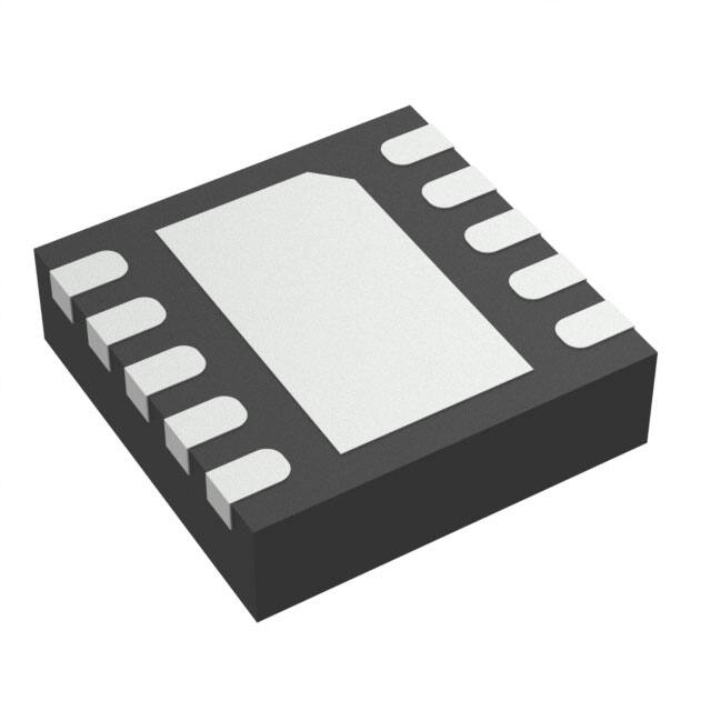
Thermally Enhanced 3 mm x 3 mm, 10-pin
SON (DRC)
Battery Powered Equipment
Notebook Computers
DESCRIPTION
The TPS51312 is a high-efficiency, synchronous,
step-down DC/DC converter. It supports 3-A
(maximum) of dc output current at output voltages
from 0.6 V to 3.3 V. The D-CAP2 mode adaptive ontime control allows a small footprint when designed
using all ceramic output capacitors and offers a low
external component count. The device also features
auto-skip function at light load condition, pre-biased
start-up and internally fixed soft-start time. When the
device is disabled, the output capacitor is discharged
through internal resistor.
The TPS51312 is available in a 3 mm x 3 mm, 10-pin
DRC package (Green RoHS compliant and Pb free)
and is specified between –40°C and 85°C.
X
SIMPLIFIED APPLICATION
CFF
RFB1
TPS51312
VIN
3.1 V to 5.5 V
C1
RFB2
EN
L1
10 VIN
SW
2
9
VIN
SW
3
8
VCC
PGOOD
4
6
FB
NC
1
5
EN
NC
7
VOUT
C2
C3
PGOOD
GND
(Thermal Pad)
UDG-12125
1
2
3
Please be aware that an important notice concerning availability, standard warranty, and use in critical applications of
Texas Instruments semiconductor products and disclaimers thereto appears at the end of this data sheet.
D-CAP2, Eco-mode are trademarks of Texas Instruments.
All other trademarks are the property of their respective owners.
PRODUCTION DATA information is current as of publication date.
Products conform to specifications per the terms of the Texas
Instruments standard warranty. Production processing does not
necessarily include testing of all parameters.
Copyright © 2012, Texas Instruments Incorporated
�TPS51312
SLUSB57 – SEPTEMBER 2012
www.ti.com
This integrated circuit can be damaged by ESD. Texas Instruments recommends that all integrated circuits be handled with
appropriate precautions. Failure to observe proper handling and installation procedures can cause damage.
ESD damage can range from subtle performance degradation to complete device failure. Precision integrated circuits may be more
susceptible to damage because very small parametric changes could cause the device not to meet its published specifications.
ORDERING INFORMATION (1)
ORDERABLE
DEVICE NUMBER
TA
PACKAGE
–40°C to 85°C
Plastic SON (DRC)
(1)
TPS51312DRCR
TPS51312DRCT
PINS
10
OUTPUT
SUPPLY
MINIMUM
QUANTITY
Tape and reel
3000
Mini reel
250
ECO PLAN
Green (RoHS and
no Pb/Br)
For the most current package and ordering information see the Package Option Addendum at the end of this document, or see the TI
web site at www.ti.com.
ABSOLUTE MAXIMUM RATINGS (1)
VALUE
Input voltage range (2)
MAX
VIN, VCC, EN
–0.3
6.0
SW
–2.0
6.0
SW (transient 20 ns)
-3.0
8.5
–1
3.6
–0.3
6.0
V
125
°C
150
°C
FB
Output voltage range (2)
PGOOD
Junction temperature, TJ
Storage temperature, Tstg
(1)
(2)
UNIT
MIN
–55
V
Stresses beyond those listed under "absolute maximum ratings" may cause permanent damage to the device. These are stress ratings
only and functional operation of the device at these or any other conditions beyond those indicated under "recommended operating
conditions" is not implied. Exposure to absolute-maximum-rated conditions for extended periods may affect device reliability.
All voltage values are with respect to the network ground terminal unless otherwise noted.
THERMAL INFORMATION
TPS51312
THERMAL METRIC (1)
UNITS
DRC (10-PIN)
θJA
Junction-to-ambient thermal resistance
42.4
θJCtop
Junction-to-case (top) thermal resistance
53.9
θJB
Junction-to-board thermal resistance
18.1
ψJT
Junction-to-top characterization parameter
1.1
ψJB
Junction-to-board characterization parameter
18.3
θJCbot
Junction-to-case (bottom) thermal resistance
6.3
°C/W
spacer - so note to thermal table has space between the note and ROC table title
(1)
For more information about traditional and new thermal metrics, see the IC Package Thermal Metrics application report, SPRA953.
RECOMMENDED OPERATING CONDITIONS
Input voltage range
Output voltage range
MIN
MAX
VIN, VCC, SW, EN
–0.1
5.5
FB
–0.1
3.5
PGOOD
–0.1
5.5
V
–40
85
°C
Operating free-air temperature, TA
2
Submit Documentation Feedback
UNIT
V
Copyright © 2012, Texas Instruments Incorporated
Product Folder Links :TPS51312
�TPS51312
www.ti.com
SLUSB57 – SEPTEMBER 2012
ELECTRICAL CHARACTERISTICS
Over operating free-air temperature range, VIN = 5 V, VCC = 5 V, VEN = 3.3 V (unless otherwise noted).
PARAMETER
TEST CONDITION
MIN
TYP
MAX
UNIT
SUPPLY VOLTAGE
VIN
Supply voltage
3.1
5.5
V
VCC
Supply voltage
3.1
5.5
V
SUPPLY CURRENT
IIN
Input voltage supply current
EN = High
100
μA
ISD
Input voltage shutdown current
EN = Low
12
μA
IVCC(in)
VCC supply current
EN = High
IVCC(sd)
VCC shutdown current
EN = Low, TA = 25°C
μA
700
20
μA
VFB REFERNCE VOLTAGE
VFBREF
Reference voltage
VFBREFTOL
Reference voltage tolerance
IFB
Feedback pin leakage current
0.6
TA = 25°C
V
–1%
1%
–100
100
nA
SMPS FREQUENCY
fSW
Switching frequency
tOFF(min)
Minimum off-time
tDEAD
Dead time (1)
0.9
110
190
SW node high, VIN = 5 V
9
SW node low, VIN = 5 V
10
MHz
270
ns
ns
LOGIC THRESHOLD AND CURRENT
VLL
EN low-level voltage
VLH
EN high-level voltage
ILLK
EN input leakage current
0.8
1.5
VIN = VCC = 3.3 V
–3
V
V
1
3
µA
MOSFET
RDS(on)_H
RDS(on)_L
On-resistance (1)
VIN = 5 V
81
VIN = 5 V
41
mΩ
SOFT-START
Soft-start time (1)
tSS
VFB rising from 0 V to 0.6 V
300
µs
PGOOD COMPARATOR
VPGTH
PGOOD threshold
tPGDLY
PGOOD high delay time
IPGLK
PGOOD leakage current
PGOOD out to higher w/r/t VFB
130%
PGOOD out to lower w/r/t VFB
50%
Delay for PGOOD in, after EN = Hi
1.3
–1
0
ms
1
μA
PROTECTIONS
Valley current limit, VIN = VCC = 3.3 V,
TA = 25°C
IOCL
Current limit threshold
VIN_UVLO
VIN UVLO threshold voltage
VCC_UVLO
VCC UVLO threshold voltage
VOVP
OVP threshold voltage
OVP detect
tOVP
OVP delay time
Overdrive = 100 mV
VUVP
UVP threshold voltage
UVP detect
tUVPDLY
UVP delay time
Overdrive = 100 mV
(1)
4.8
A
Wake-up
2.85
2.95
3.05
Shutdown
2.6
2.7
2.8
Wake-up
2.85
2.95
3.05
Shutdown
2.6
2.7
2.8
V
V
130%
1.9
µs
50%
2.4
µs
Specified by design. Not production tested.
Submit Documentation Feedback
Copyright © 2012, Texas Instruments Incorporated
Product Folder Links :TPS51312
3
�TPS51312
SLUSB57 – SEPTEMBER 2012
www.ti.com
ELECTRICAL CHARACTERISTICS (continued)
Over operating free-air temperature range, VIN = 5 V, VCC = 5 V, VEN = 3.3 V (unless otherwise noted).
PARAMETER
TEST CONDITION
MIN
TYP
MAX
UNIT
SW PULL-DOWN RESISTANCE
RSWPD
SW pull-down resistance
EN = Lo
260
Shutdown temperature
145
Ω
THERMAL SHUTDOWN
Thermal shutdown threshold (2)
TSDN
(2)
Hysteresis
°C
20
Specified by design. Not production tested.
DEVICE INFORMATION
FUNCTIONAL BLOCK DIAGRAM
TPS51312
VREF – 50%
+
PGOOD
UV
VBG
Delay
VREF
VREF
+
30%
+
OV
UVP
FB
Σ
+
VSW
OVP
+
ENOK
EN
1.5 V/ 0.8 V
Control Logic
PWM
+
IGAIN
+
·
·
·
·
·
On/Off Time
Minimum On /Off
SKIP Mode
OCL/OVP/UVP
Discharge
+
VCCOK
VCC UVLO
VCC
2.95 V/ 2.7 V
+
VINOK
VIN UVLO
2.95 V/2.7 V
VIN
VBG
OC
+
+
tON
One Shot
XCON
SW
Discharge
+
ZC
UDG-12124
4
Submit Documentation Feedback
Copyright © 2012, Texas Instruments Incorporated
Product Folder Links :TPS51312
�TPS51312
www.ti.com
SLUSB57 – SEPTEMBER 2012
DRC PACKAGE
10 PINS
(TOP VIEW)
NC
1
SW
2
9
VIN
SW
3
8
VCC
PGOOD
4
7
NC
EN
5
6
FB
10 VIN
GND
.
.
PIN FUNCTIONS
PIN
NAME
NO.
I/O
DESCRIPTION
EN
5
I
Enable function for the switched-mode power supply (SMPS) (3.3-V logic compatible)
FB
6
I
Voltage feedback. Also used for OVP, UVP and PGOOD determination.
–
No connection. Make no external connection to this pin.
O
Power good indicator. Requires external pull-up resistor.
I
Switching node output. Connect to external inductor. Also serve as current sensing negative input for over
current protection purpose
I
Power supply for analog circuit.
I
Main power conversion input and gate-drive voltage supply for output FETs.
I
Ground terminal.
NC
PGOOD
SW
VCC
VIN
Thermal Pad
1
7
4
2
3
8
9
10
Submit Documentation Feedback
Copyright © 2012, Texas Instruments Incorporated
Product Folder Links :TPS51312
5
�TPS51312
SLUSB57 – SEPTEMBER 2012
www.ti.com
100
100
90
90
80
80
70
70
Efficiency (%)
Efficiency (%)
TYPICAL CHARACTERISTICS
60
50
40
60
50
40
30
30
20
20
0
VOUT = 1.5 V
fSW = 900 kHz
VIN = 5 V
VIN = 3.3 V
10
1
10
100
Output Current (mA)
1000
0
10000
1
10
G000
Figure 1. Efficiency vs. Output Current
1.810
90
1.808
Output Voltage (V)
Efficiency (%)
80
70
60
50
40
30
VIN = 5 V
VOUT = 3.3 V
fSW = 900 kHz
10
0
1
10
100
Output Current (mA)
1000
100
Output Current (mA)
1000
10000
G000
Figure 2. Efficiency vs. Output Current
100
20
VOUT = 1.8 V
fSW = 900 kHz
VIN = 5 V
VIN = 3.3 V
10
VIN = 5 V
VIN = 3.3 V
1.806
1.804
1.802
1.800
1.798
1.796
VOUT =1.8 V
10000
1.794
0.0
0.5
1.0
1.5
2.0
Output Current (A)
G000
Figure 3. Efficiency vs. Output Current
2.5
3.0
G001
Figure 4. DC Load Regulation
400
60
VIN = 3.3 V
ILOAD = 3 A
VVOUT = 1.05 V
fSW = 900 kHz
40
350
300
200
150
0
Phase (°)
Gain (dB)
250
20
100
50
−20
Magnitude
−40
100
1000
0
Phase
10000
100000
Frequency (Hz)
1000000
−50
10000000
G000
Figure 5. Bode Plot
6
Submit Documentation Feedback
Copyright © 2012, Texas Instruments Incorporated
Product Folder Links :TPS51312
�TPS51312
www.ti.com
SLUSB57 – SEPTEMBER 2012
TYPICAL CHARACTERISTICS (continued)
Figure 6. 3.3-V Input, 1.8-V Output from 0 A to 3 A
Figure 7. 5-V Input, 1.8-V Output from 0 A to 3 A
Figure 8. 5-V Input, 1.8-V Output Start-Up
Submit Documentation Feedback
Copyright © 2012, Texas Instruments Incorporated
Product Folder Links :TPS51312
7
�TPS51312
SLUSB57 – SEPTEMBER 2012
www.ti.com
APPLICATION INFORMATION
Functional Overview
TPS51312 is a D-CAP2 mode adaptive on time converter with internal integrator. Monolithically integrate high
side and low side FET supports output current to a maximum of 3-ADC. The converter automatically runs in
discontinuous conduction mode to optimize light load efficiency. A switching frequency of 900 kHz enables
optimization of the power train for the cost, size and efficiency performance of the design.
PWM Operation
The PWM operation is comprised of three separate loops, A, B and C as shown in Figure 9.
L OUT
VIN
C OUT
+
–
R LOAD
Integrator
VCS
PWM
Comparator
Q
S
Q
R
Σ
VC
+
+
RFB 1
+
gM
VFB
RFB 2
VREF
+
–
tON
OneShot
+
–
B
C
RA
R 11
CSN
K1
+
CA
RB
CSP
R12
CB
A
UDG-12133
Figure 9. ¾PWM Operation
Internal Current Loop (A)
Loop A is the internal current loop. The current information is sampled, divided and averaged at the SW node.
The RC time constant and the gain of the current sense amplifier is chosen to cover the wide range of power
stage design intended for this application.
Internal Voltage Loop (B)
Loop B is the internal voltage loop. The feedback voltage information is compared to the voltage reference at the
input of the gM amplifier, the internal integrator is designed to provide a zero at the double pole location to boost
phase margin at the desired crossover frequency.
8
Submit Documentation Feedback
Copyright © 2012, Texas Instruments Incorporated
Product Folder Links :TPS51312
�TPS51312
www.ti.com
SLUSB57 – SEPTEMBER 2012
Fast Feedforward Loop (C)
Loop C is the additional loop that acts a direct fast feedforward loop to enhance the transient response.
In steady state operation as shown in Figure 10, the on time is initiated by the interaction of the three loops
mentioned above. When the (VC– VCS) is rising above threshold defined by (VFB – VREF), the PWM comparator
issues the on time pulse after the propagation delay. The demand of on time occurs when the artificial current
has reached the valley point. The load regulation is maintained by the integrator provided by the gM amplifier and
integrator.
In transient operation as shown in Figure 11, the benefit of this topology is becoming evident. In an all MLCC
output configuration, especially when the output capacitance is low, when the load step is applied, the output
voltage is immediately discharged to try to keep the load demand. The immediate reflection of the load demand
is instantly reflected in the FB voltage. The (VFB – VREF) is thus served as a termination voltage level for the
(VC – VCS), thus modulating the initiation of the on time. The transient response can be improved further by
amplifying the difference between VFB and the VREF reference.
VFB–VREF
ILOAD
VC – VCS
IL
tON
PWM
PWM delay ~100 ns
PWM
IL
VFB –VREF
VOUT
VC – VCS
UDG-12114
Figure 10. Steady-State Operation
UDG-12115
Figure 11. Transient Operation
PWM Frequency
The TPS51312 operates at a switching frequency of 900 kHz.
Light Load Power Saving Features
The TPS51312 offers an automatic pulse-skipping feature to provide excellent efficiency over the entire load
range. The converter senses the current during low side FET on and prevents negative current flow by turning off
the low side FET. This saves power by eliminating re-circulation of the inductor current. When the bottom FET is
turned off, the converter enters discontinuous mode, and the switching frequency decreases, reducing switching
loss.
Power Sequences
TPS51312 initiates the soft-start process when the EN, VIN and VCC pins are ready. The soft-start time 300 µs
when the reference voltage is between 0 V and 0.6 V (VREF). The actual voltage ramp up time is the same as
that of the VREF start-up time, which is 300 µs.
Power Good Signal
The TPS51312 has one open-drain power good (PGOOD) pin. During initial startup, there is a 1.3-ms power
good high propagation delay after EN goes high. The PGOOD de-asserts when the EN is pulled low or an
undervoltage condition on VCC or VIN or any other faults (such as VOUT, UVP, OCP, OVP) that require latch off
action is detected.
Protection Features
The TPS51312 offers many features to protect the converter power chain as well as the system electronics.
Submit Documentation Feedback
Copyright © 2012, Texas Instruments Incorporated
Product Folder Links :TPS51312
9
�TPS51312
SLUSB57 – SEPTEMBER 2012
www.ti.com
Input Undervoltage Protection on VCC and VIN (UVLO)
The TPS51312 continuously monitor the voltage on the VCC and VIN to ensure the voltage level is high enough to
bias the converter properly and to provide sufficient gate drive potential to maintain high efficiency for the
converter. The converter starts with VCC and VIN approximately 2.95 V and has a nominal of 250 mV of
hysteresis, assuming EN is above the logic threshold level. If the UVLO level is reached for either VCC or VIN, the
converter transitions the SW node into a tri-state and remains off until the device is reset by both VCC and VIN
reaches 2.95 V (nominal). The PGOOD is deasserted when UVLO is detected and remains low until the device is
reset.
Output Overvoltage Protection (OVP)
The TPS51312 has OVP protection circuit. An OVP event is detected when the FB voltage is approximately
130% x 0.6VREF. In this case, the converter de-asserts the PGOOD signal and performs the overvoltage
protection function. The converter latches off both high-side and low-side FET and remains in this state after a
delay of 1.9 µs (typ) until the device is reset by EN, or VCC or VIN.
Output Undervoltage Protection (UVP)
Output undervoltage protection works in conjunction with the current protection described in the Overcurrent and
Current Limit Protection section. If the FB voltage drops below 50% x 0.6 VREF, after a delay of 2.4 µs (typ), the
converter latches off. Undervoltage protection can be reset by EN, VCC or VIN.
Overcurrent and Current Limit Protection
The TPS51312 provides an overcurrent protection function. The nominal OCP is 4.8-A DC. When the current
limit is exceeded for consecutive 9 cycles, the converter latches off and remains latched off until it is reset by EN,
VCC or VIN.
The TPS51312 also provides current limit protection function. If the sense current is above the OCL setting, the
converter delays the next on pulse until the current level drops below the OCL limit. Current limiting occurs on a
pulse-by-pulse basis. During a fast or very fast overcurrent event, the output voltage tends to droop until the UVP
limit is reached. Then the converter de-asserts the PGOOD signal, and latches off after a typical delay time of
2.4 µs. The converter remains in this state until the device is reset by EN, VCC or VIN.
Thermal Protection
The TPS51312 has an internal temperature sensor. When the die temperature reaches a nominal of 145°C, the
device shuts down until the temperature cools by approximately 20°C. Then the converter restarts. The thermal
shutdown is an non-latched behavior.
10
Submit Documentation Feedback
Copyright © 2012, Texas Instruments Incorporated
Product Folder Links :TPS51312
�TPS51312
www.ti.com
SLUSB57 – SEPTEMBER 2012
REFERENCE DESIGN
Application Schematic
Figure 12 shows the application schematic..
C FF
47 mF
R FB1
40 kW
L1
1 mH
TPS51312
VIN
3.1 V to 5.5 V
SW
2
SW
3
PGOOD
4
NC
1
NC
7
10 VIN
C1
10 mF
R FB2 EN
20 kW
9
VIN
8
VCC
6
FB
5
EN
VOUT
1.8 V
PGOOD
C2
22 mF
C3
22 mF
GND
(Thermal Pad )
UDG-12145
Figure 12. Reference Design Schematic
Table 1. Reference Design List of Materials
FUNCTION
MANUFACTURER
PART NUMBER
Output Inductor
Vishay
IHLP-2020BZ-01
Panasonic
ECJ2FB0J226M
Murata
GRM21BR60J226ME39L
Ceramic Output Capacitors
Design Procedure
Step One. Determine the specifications.
• VOUT = 1.8 V
• ICC(max) = 3 A
• di/dt = 2.5 A/µs
Step Two. Determine the system parameters.
The input voltage range and operating frequency are of primary interest. For example,
• VIN = VCC = 5 V
• fSW = 900 kHz.
Submit Documentation Feedback
Copyright © 2012, Texas Instruments Incorporated
Product Folder Links :TPS51312
11
�TPS51312
SLUSB57 – SEPTEMBER 2012
www.ti.com
Step Three. Set the output voltage.
Use Equation 1 to determine the output voltage.
æR
+ RFB2 ö
VOUT = VREF ´ ç FB1
÷
RFB2
è
ø
(1)
The output voltage is determined by VREF (0.6 V) and the resistor dividers (RFB1 and RFB2). The output voltage
is regulated to the FB pin. For the current reference design of 1.8 V, select 40 kΩ as the value for RFB1 and
20 kΩ as the value of RFB2 (see Figure 12). As a recommendation, choose a value of less 50 kΩ both resisters.
Place a 47-pF, feedford capacitor in parallel with RFB1 to help reduce the output voltage ripple during the
transition from DCM to CCM.
Step Four. Determine inductor value and choose inductor.
Smaller inductance yields better transient performance but the consequence is higher ripple and lower efficiency.
Higher values have the opposite characteristics. It is common practice to limit the ripple current to 25% to 50% of
the maximum current. In this case, use 40%:
IP-P = 3 A ´ 0.4 = 1.2 A
where
•
•
•
fSW = 900 kHz
VIN = 5 V
VOUT = 1.8 V
(2)
ö
V ´ dT æ (VIN - VOUT ) ö æ VOUT
L=
=ç
÷´ç
÷ = 1mH
ç
÷ ç (fSW ´ VIN ) ÷
IP-P
IP-P
è
ø è
ø
(3)
For this application, choose a 1-µH, 18.9-mΩ inductor from Vishay part number IHLP-2020BZ-01.
Step Five. Determine the output capacitance.
To determine COUT based on transient and stability requirement, first calculate the minimum output capacitance
for a given transient.
Equation 4 and Equation 5 calculate the minimum output capacitance for meeting the transient requirement.
æV
ö
´t
L ´ DILOAD(max )2 ´ ç VOUT SW + tMIN(off ) ÷
ç VIN(min )
÷
è
ø
COUT(min_ under ) =
ææ V
ö
ö
IN(min ) - VVOUT
÷
÷ ´ tSW - t
2 ´ DVLOAD(insert ) ´ ç ç
MIN(off ) ÷ ´ VVOUT
çç
÷
VIN(min )
ø
èè
ø
COUT(min_ over ) =
(4)
2
(
LOUT ´ DILOAD(max )
)
2 ´ DVLOAD(release ) ´ VVOUT
(5)
Table 2. Choosing Output Inductors and Output Capacitors
TEMPERATURE
–10°C ≤ TA ≤ 85°C
–40°C ≤ TA ≤ 85°C
12
OUTPUT
CAPACITORS
OUTPUT
VOLTAGE
VOUT (V)
INDUCTANCE
LOUT (µH)
1.5
1
1
1.8
1
1
3.3
2.2
2
1.5
1
2
1.8
1
2
3.3
2.2
3
NUMBER
Submit Documentation Feedback
VALUE (µF)
FAST
FEEDFORWARD
CAPACITOR
CFF (pF)
22
47
Copyright © 2012, Texas Instruments Incorporated
Product Folder Links :TPS51312
�TPS51312
www.ti.com
SLUSB57 – SEPTEMBER 2012
Step Six. Establishing the internal compensation loop.
The TPS51312 is designed with an internal compensation loop. The internal integrator zero location is
approximately 60 kHz. During the time that the power stage double pole frequency contributed by the LOUT and
COUT is less than or equal to that of the zero location, the converter is stable with sufficient margin.
Step Seven. Select decoupling and peripheral components.
For TPS51312 peripheral capacitors use the following minimum value of ceramic capacitance, X5R or better
temperature coefficient is recommended. Tighter tolerances and higher voltage ratings are always appropriate.
VCC and VIN decoupling ≥ 2 × 10 µF, 6.3 V
Pull up resistor on PGOOD = 100 kΩ
Layout Considerations
Good layout is essential for stable power supply operation. Follow these guidelines for an efficient PCB layout.
• Place VIN, VCC decoupling capacitors as close to the device as possible.
• Use wide traces for the VIN, SW and GND pins. These nodes carry high current and also serve as heat
sinks.
• Place FB and voltage setting dividers as close to the device as possible.
• Place an R-C network from SW to GND to help to reduce the voltage spikes on the SW pin.
Submit Documentation Feedback
Copyright © 2012, Texas Instruments Incorporated
Product Folder Links :TPS51312
13
�PACKAGE OPTION ADDENDUM
www.ti.com
10-Dec-2020
PACKAGING INFORMATION
Orderable Device
Status
(1)
Package Type Package Pins Package
Drawing
Qty
Eco Plan
(2)
Lead finish/
Ball material
MSL Peak Temp
Op Temp (°C)
Device Marking
(3)
(4/5)
(6)
TPS51312DRCR
ACTIVE
VSON
DRC
10
3000
RoHS & Green
NIPDAU
Level-2-260C-1 YEAR
-40 to 85
S51312
TPS51312DRCT
ACTIVE
VSON
DRC
10
250
RoHS & Green
NIPDAU
Level-2-260C-1 YEAR
-40 to 85
S51312
(1)
The marketing status values are defined as follows:
ACTIVE: Product device recommended for new designs.
LIFEBUY: TI has announced that the device will be discontinued, and a lifetime-buy period is in effect.
NRND: Not recommended for new designs. Device is in production to support existing customers, but TI does not recommend using this part in a new design.
PREVIEW: Device has been announced but is not in production. Samples may or may not be available.
OBSOLETE: TI has discontinued the production of the device.
(2)
RoHS: TI defines "RoHS" to mean semiconductor products that are compliant with the current EU RoHS requirements for all 10 RoHS substances, including the requirement that RoHS substance
do not exceed 0.1% by weight in homogeneous materials. Where designed to be soldered at high temperatures, "RoHS" products are suitable for use in specified lead-free processes. TI may
reference these types of products as "Pb-Free".
RoHS Exempt: TI defines "RoHS Exempt" to mean products that contain lead but are compliant with EU RoHS pursuant to a specific EU RoHS exemption.
Green: TI defines "Green" to mean the content of Chlorine (Cl) and Bromine (Br) based flame retardants meet JS709B low halogen requirements of