Sample &
Buy
Product
Folder
Support &
Community
Tools &
Software
Technical
Documents
TPS51604-Q1
SLUSBT2A – JANUARY 2014 – REVISED AUGUST 2014
TPS51604-Q1 Synchronous Buck FET Driver for High-Frequency
CPU Core Power in Automotive Applications
1 Features
3 Description
•
•
The TPS51604-Q1 drivers are optimized for highfrequency CPU VCORE applications. Advanced
features such as reduced dead-time drive and auto
zero crossing are used to optimize efficiency over the
entire load range.
1
•
•
•
•
•
•
•
•
Qualified for Automotive Applications
AEC-Q100 Qualified With the Following Results:
– Device Temperature Grade 1: –40°C to 125°C
– Device Human Body Model ESD Classification
Level H2
– Device Charged Device Model ESD
Classification Level C3B
Reduced Dead-Time Drive Circuit for Optimized
CCM
Automatic Zero Crossing Detection for Optimized
DCM Efficiency
Multiple Low-Power Modes for Optimized LightLoad Efficiency
Optimized Signal Path Delays for High-Frequency
Operation
Integrated BST Switch Drive Strength Optimized
for Ultrabook FETs
Optimized for 5-V FET Drive
Conversion Input Voltage Range (VIN): 4.5 to 28 V
2-mm × 2-mm, 8-Pin, WSON Power-Pad Package
The SKIP pin provides immediate CCM operation to
support controlled management of the output voltage.
In addition, the TPS51604-Q1 supports two lowpower modes. With the PWM input in 3-state,
quiescent current is reduced to 130 µA, with
immediate response. When SKIP is held at 3-state,
the current is reduced to 8 µA (typically 20 µs is
required to resume switching). Paired with the
appropriate TI controller, the drivers deliver an
exceptionally high performance power supply system.
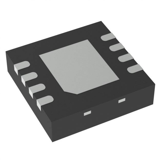
The TPS51604-Q1 device is packaged in a space
saving, thermally-enhanced 8-pin, 2-mm x 2-mm
WSON package and operates from –40°C to 125°C.
Device Information(1)
PART NUMBER
TPS51604-Q1
WSON (8)
BODY SIZE (NOM)
2.00 mm × 2.00 mm
(1) For all available packages, see the orderable addendum at
the end of the data sheet.
2 Applications
•
PACKAGE
Automotive Rear Seat Entertainment (RSE)
Tablets Using High-Frequency CPUs With the
Following Power Input:
– Adapter
– Battery
– NVDC
– 5-V or 12-V Rails
Simplified Schematic
R1
C3
VIN
TPS51604-Q1
Q1
1
BST
DRVH
8
PWM
2
PWM
SW
7
SKIP
3
SKIP
GND
6
VDD
4
VDD
DRVL
5
Q2
L1
C1
C2
C4
UDG-12234
1
An IMPORTANT NOTICE at the end of this data sheet addresses availability, warranty, changes, use in safety-critical applications,
intellectual property matters and other important disclaimers. PRODUCTION DATA.
�TPS51604-Q1
SLUSBT2A – JANUARY 2014 – REVISED AUGUST 2014
www.ti.com
Table of Contents
1
2
3
4
5
6
Features ..................................................................
Applications ...........................................................
Description .............................................................
Revision History.....................................................
Pin Configuration and Functions .........................
Specifications.........................................................
1
1
1
2
3
4
6.1
6.2
6.3
6.4
6.5
6.6
4
4
4
4
5
7
Absolute Maximum Ratings .....................................
Handling Ratings.......................................................
Recommended Operating Conditions.......................
Thermal Information ..................................................
Electrical Characteristics...........................................
Typical Characteristics ..............................................
6.7 Typical Power Block MOSFET Characteristics......... 9
7
Detailed Description ............................................ 10
7.1 Overview ................................................................. 10
7.2 Functional Block Diagram ....................................... 10
7.3 Feature Description................................................. 10
8
Layout ................................................................... 14
9
Device and Documentation Support.................. 15
8.1 Layout Guidelines ................................................... 14
9.1 Trademarks ............................................................. 15
9.2 Electrostatic Discharge Caution .............................. 15
9.3 Glossary .................................................................. 15
10 Mechanical, Packaging, and Orderable
Information ........................................................... 15
4 Revision History
Changes from Original (January 2014) to Revision A
Page
•
Added Handling Ratings table, Feature Description section, Layout section, Device and Documentation Support
section, and Mechanical, Packaging, and Orderable Information section.............................................................................. 1
•
Updated device name in Thermal Information ...................................................................................................................... 4
•
Corrected temperature range for Electrical Characteristics specifications from 105°C to 125°C .......................................... 5
•
Corrected temperature range for Electrical Characteristics specifications from 105°C to 125°C .......................................... 6
2
Submit Documentation Feedback
Copyright © 2014, Texas Instruments Incorporated
Product Folder Links: TPS51604-Q1
�TPS51604-Q1
www.ti.com
SLUSBT2A – JANUARY 2014 – REVISED AUGUST 2014
5 Pin Configuration and Functions
DSG
8 PINS
(TOP VIEW)
BST 1
8 DRVH
PWM 2
7 SW
TPS51604-Q1
SKIP
3
6 GND
VDD
4
5 DRVL
Pin Functions
PIN
NAME
NO.
I/O (1)
DESCRIPTION
BST
1
I
High-side N-channel FET bootstrap voltage input; power supply for high-side driver
DRVH
8
O
High-side N-channel gate drive output
DRVL
5
O
Synchronous low-side N-channel gate drive output
GND
6
—
Synchronous low-side N-channel gate drive return and IC reference
PWM
2
I
PWM input. A tri-state voltage on this pin turns OFF both the high-side (DRVH) and low-side drivers (DRVL)
SKIP
3
I
When SKIP is LO, the zero crossing comparator is active; the power chain enters discontinuous conduction
mode when the inductor current reaches zero. When SKIP is HI, the zero crossing comparator is disabled,
and the driver outputs follow the PWM input. A tri-state voltage on SKIP puts the driver into a very-low power
state.
SW
7
I/O
High-side N-channel gate drive return. Also, zero-crossing sense input
—
Tie to system GND plane with multiple vias
Thermal Pad
VDD
(1)
4
I
5-V power supply input; decouple to GND with a ceramic capacitor with a value of 1 µF or greater
I = Input, O = Output
Submit Documentation Feedback
Copyright © 2014, Texas Instruments Incorporated
Product Folder Links: TPS51604-Q1
3
�TPS51604-Q1
SLUSBT2A – JANUARY 2014 – REVISED AUGUST 2014
www.ti.com
6 Specifications
6.1 Absolute Maximum Ratings (1)
(2)
over operating free-air temperature (unless otherwise noted)
Input voltage
Output voltage
Ground pins
MIN
MAX
VDD
–0.3
6
PWM, SKIP
–0.3
6
BST
–0.3
35
BST (transient
很抱歉,暂时无法提供与“TPS51604QDSGRQ1”相匹配的价格&库存,您可以联系我们找货
免费人工找货