www.ti.com
Table of Contents
User’s Guide
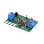
TPS53014 Buck Controller Evaluation Module User's
Guide
Table of Contents
1 Introduction.............................................................................................................................................................................2
2 Description.............................................................................................................................................................................. 2
2.1 Typical Applications............................................................................................................................................................2
2.2 Features............................................................................................................................................................................. 2
3 Electrical Performance Specifications................................................................................................................................. 3
4 Schematic................................................................................................................................................................................4
5 Test Setup................................................................................................................................................................................5
5.1 Test Equipment.................................................................................................................................................................. 5
5.2 Recommended Test Setup.................................................................................................................................................6
6 Configurations........................................................................................................................................................................ 6
6.1 Enable/Disable Switch S1.................................................................................................................................................. 6
7 Test Procedure........................................................................................................................................................................ 7
7.1 Line/Load Regulation and Efficiency Measurement Procedure......................................................................................... 7
7.2 List of Test Points............................................................................................................................................................... 7
7.3 Equipment Shutdown......................................................................................................................................................... 7
8 Performance Data and Typical Characteristic Curves........................................................................................................ 8
8.1 Efficiency............................................................................................................................................................................8
8.2 Load Regulation................................................................................................................................................................. 8
8.3 Line Regulation.................................................................................................................................................................. 9
8.4 Load Transient................................................................................................................................................................... 9
8.5 Output Ripple................................................................................................................................................................... 10
8.6 Switching Node.................................................................................................................................................................11
8.7 Enable Start-Up................................................................................................................................................................12
8.8 Disable............................................................................................................................................................................. 12
8.9 Thermal Image................................................................................................................................................................. 13
9 EVM Assembly Drawing and PCB Layout.......................................................................................................................... 14
10 List of Materials.................................................................................................................................................................. 17
11 Revision History..................................................................................................................................................................17
SLUU943A – MAY 2012 – REVISED DECEMBER 2021
Submit Document Feedback
TPS53014 Buck Controller Evaluation Module User's Guide
Copyright © 2021 Texas Instruments Incorporated
1
�Introduction
www.ti.com
1 Introduction
The TPS53014EVM-126 evaluation module (EVM) presents an easy-to-use reference design for a typical pointof-load application in a standalone module using the TPS53014 controller in cost-sensitive applications.
2 Description
The TPS53014EVM-126 provides the user with a convenient way to evaluate the TPS53014 D-CAP2™ mode
control in a cost sensitive application. Providing a 1.05-V output at up to 8 A from a loosely regulated 12-V (8
V – 22 V) source, the TPS53014EVM-126 is designed to demonstrate the TPS53014 in a typical point-of-load
application while providing a number of test points to evaluate the performance of the TPS53014.
2.1 Typical Applications
•
Point-of-load regulations in low-power systems for a wide range of applications
– Digital TV power supply
– Network home terminals
– Digital set top box (STB)
– DVD player/recorder
– Game consoles and others
2.2 Features
The TPS53014EVM-126 features:
•
•
•
•
•
•
•
•
2
D-CAP2™ mode control
– Fast transient response
– No external parts required for loop compensation
– Compatible with ceramic output capacitors
Auto-skip Eco-mode™ for high efficiency at light load
500-kHz switching frequency
Adjustable soft start
Non-sinking pre-biased soft start
Cycle-by-cycle overcurrent limit
Overcurrent, overvoltage, undervoltage, and overtemperature protections
Convenient test points for probing critical waveforms
TPS53014 Buck Controller Evaluation Module User's Guide
Copyright © 2021 Texas Instruments Incorporated
SLUU943A – MAY 2012 – REVISED DECEMBER 2021
Submit Document Feedback
�www.ti.com
Electrical Performance Specifications
3 Electrical Performance Specifications
Table 3-1. TPS53014EVM-126 Electrical Performance Specifications
PARAMETER
TEST CONDITIONS
MIN
TYP
MAX
UNITS
Input Characteristics
Voltage range
VIN
8.0
12
22
V
Maximum input current
VIN = 12 V, IOUT = 8 A
0.9
A
No load input current
VIN = 12 V, IOUT = 0 A
0.6
mA
1.05
V
Output Characteristics
Output voltage
Output voltage regulation
Setpoint accuracy
(VIN = 12 V, IOUT = 8 A)
–2%
Line regulation
(VIN = 8.0 V – 22 V, IOUT = 8 A)
1%
Load regulation
(VIN = 12 V, IOUT = 0 A – 8 A)
Output voltage ripple
1.5%
VIN = 12 V, IOUT = 8 A
20
Output load current
Overcurrent limit
2%
0
VIN = 12 V
mVpp
8.0
A
11
Systems Characteristics
Switching frequency
500
Peak efficiency
VIN = 12 V, IOUT = 3.2 A
86.5%
Full load efficiency
VIN = 12 V, IOUT = 8.0 A
81.4%
Operating temperature
SLUU943A – MAY 2012 – REVISED DECEMBER 2021
Submit Document Feedback
25
kHz
°C
TPS53014 Buck Controller Evaluation Module User's Guide
Copyright © 2021 Texas Instruments Incorporated
3
�4
Disable (Default)
Enable
VIN
1.00k
R8
1.00k
R6
6
4
5
1
2
4.7uF
C11
140
R11
J1
VREG5
TP3
AGND
EN
TP5
S1
SW_G12AP
Enable Circuitry
SS
TP4
VOUT
PWRGND
VIN
8V - 22V
GND
VIN
VIN
0.01uF
C10
1
R4
R3
SH1
TPS53014 Buck Controller Evaluation Module User's Guide
Copyright © 2021 Texas Instruments Incorporated
C1
C13
TP9
GND
0.1uF
5
4
3
2
1
SS
VIN
EN
6
7
8
9
10
D1
BAT54XV2T1
PGND
DRVL
SW
DRVH
VBST
NOT POPULATED
1
C4
VREG5
1
C2
10uF
U1
TPS53014DGS
VFB
10uF
Notes:
23.7k
8.66k
R1
TP2
GND
VIN
TP1
C3
2.05
R7
5.11
R5
10uF
15.4k
R10
C5
G
S
D
G
S
Q2 D
CSD17507Q5A
0.1uF
10.0
R2
TP10
1000pF
C12
3.01
R9
SW
TP6
Q1
CSD17507Q5A
1.5uH
L1
22uF
C6
22uF
C7
1
C8
1
C9
TP8
GND
VOUT
TP7
GND
VOUT
1.05V/8A
J2
PWRGND
1
2
VOUT
Schematic
www.ti.com
4 Schematic
Figure 4-1. TPS53014EVM-126 Schematic
SLUU943A – MAY 2012 – REVISED DECEMBER 2021
Submit Document Feedback
�www.ti.com
Test Setup
5 Test Setup
5.1 Test Equipment
Voltage Source:
• VIN: The input voltage source, VIN, should be a 0-V to 30-V variable DC source capable of supplying 2 ADC.
Connect VIN to J1 as shown in Figure 5-2.
Multimeters:
• V1: VIN at TP1 (VIN) and TP2 (GND), 0-V to 30-V voltmeter
• V2: VOUT at TP7 (VOUT) and TP8 (GND)
• A1: VIN input current, 0-ADC to 2-ADC Ammeter
Output Load: The output load should be an electronic constant resistance mode load capable of 0 ADC to 8 ADC
at 1.05 V.
Oscilloscope: A digital or analog oscilloscope can be used to measure the output ripple. The oscilloscope
should be set for the following:
• 1-MΩ impedance
• 20-MHz bandwidth
• AC coupling
• 1-µs/division horizontal resolution
• 50-mV/division vertical resolution
Test points TP7 and TP8 can be used to measure the output ripple voltage by placing the oscilloscope probe tip
through TP7 and holding the ground barrel on TP8 as shown in Figure 5-1. Using a leaded ground connection
may induce additional noise due to the large ground loop.
TP7
TP8
Figure 5-1. Tip and Barrel Measurement for VOUT Ripple
Fan: Some of the components in this EVM may approach temperatures of 85°C during operation. A small
fan capable of 200 LFM to 400 LFM is recommended to reduce component temperatures while the EVM is
operating. The EVM should not be probed while the fan is not running.
Recommended Wire Gauge:
• VIN to J1: The recommended wire size is 1x AWG #16 per input connection, with the total length of wire less
than four feet (2 feet input, 2 feet return).
• J2 to LOAD: The minimum recommended wire size is 1x AWG #16, with the total length of wire less than
four feet (2 feet output, 2 feet return)
SLUU943A – MAY 2012 – REVISED DECEMBER 2021
Submit Document Feedback
TPS53014 Buck Controller Evaluation Module User's Guide
Copyright © 2021 Texas Instruments Incorporated
5
�Test Setup
www.ti.com
5.2 Recommended Test Setup
Figure 5-2 is the recommended test setup to evaluate the TPS53014EVM-126. Working at an ESD workstation,
make sure that any wrist straps, bootstraps, or mats are connected referencing the user to earth ground before
power is applied to the EVM.
Figure 5-2. TPS53014EVM-126 Recommended Test Setup
Input Connections:
• Prior to connecting the DC input source VIN, it is advisable to limit the source current from VIN to 2-A
maximum. Make sure VIN is initially set to 0 V and connected to J2 as shown in Figure 5-2.
• Connect a current meter A1 between VIN and J1 to measure the input current.
• Connect a voltmeter V1 at TP1 (VIN) and TP2 (GND) to measure the input voltage.
Output Connections:
• Connect Load to J2 and set load to constant resistance mode to sink 0 ADC before VIN is applied.
• Connect a voltmeter V2 at TP7 (VOUT) and TP8 (GND) to measure the output voltage.
Other Connections: Place a fan as shown in Figure 5-2 and turn on, making sure air is flowing across the EVM.
6 Configurations
6.1 Enable/Disable Switch S1
The TPS53014EVM-126 is equipped with a switch (S1) to drive the EN pin of the TPS53014. When S1 is
in the Enable position, EN is connected to VIN, and the TPS53014 is enabled and generates a regulated
1.05-V output. When S1 is in the Disable position, EN is connected to GND, and the TPS53014 enters a high
impedance output state.
Default setting: Set S1 to the Disabled position to disable the controller
6
TPS53014 Buck Controller Evaluation Module User's Guide
Copyright © 2021 Texas Instruments Incorporated
SLUU943A – MAY 2012 – REVISED DECEMBER 2021
Submit Document Feedback
�www.ti.com
Test Procedure
7 Test Procedure
7.1 Line/Load Regulation and Efficiency Measurement Procedure
1.
2.
3.
4.
5.
6.
7.
8.
9.
10.
11.
Set up the EVM as described in Section 5 and Figure 5-2.
Ensure Load is set to constant resistance mode and to sink 0 ADC.
Ensure the switch S1 is set per Section 6.
Increase VIN from 0 V to 12 V. Using V1 to measure VIN voltage.
Set the switch S1 to Enable position to enable the controller.
Use V2 to measure VOUT voltage, A1 to measure VIN current.
Vary load from 0 ADC to 8 ADC. VOUT should remain in load regulation.
Vary VIN from 8.0 V to 22 V. VOUT should remain in line regulation.
Set the switch S1 to Disable position to disable the controller.
Decrease load to 0 A.
Decrease VIN to 0 V.
7.2 List of Test Points
Table 7-1. Test Point Functions
TEST POINTS
NAME
TP1
VIN
Input voltage
DESCRIPTION
TP2
GND
GND
TP3
VREG5
Output of 5-V linear regulator
TP4
SS
Soft-start ramp voltage
TP5
EN
Enable pin
TP6
SW
Switching node
TP7
VOUT
Output voltage
TP8
GND
GND
TP9
GND
GND
TP10
GND
GND
7.3 Equipment Shutdown
1. Shut down VIN.
2. Shut down Load.
3. Shut down FAN.
SLUU943A – MAY 2012 – REVISED DECEMBER 2021
Submit Document Feedback
TPS53014 Buck Controller Evaluation Module User's Guide
Copyright © 2021 Texas Instruments Incorporated
7
�Performance Data and Typical Characteristic Curves
www.ti.com
8 Performance Data and Typical Characteristic Curves
Figure 8-1 through Figure 8-11 present typical performance curves for TPS53014EVM-126.
8.1 Efficiency
100
90
Efficiency - %
80
70
60
50
40
VIN = 8 V
30
20
VIN = 12 V
10
VIN = 22 V
0
0.001
0.010
0.100
1.000
10.000
ILOAD - Load Current - A
Figure 8-1. Efficiency
8.2 Load Regulation
VOUT - Output Voltage - V
1.1
1.08
1.06
VIN = 8 V
1.04
VIN = 12 V
1.02
VIN = 22 V
1
0.001
0.010
0.100
1.000
10.000
ILOAD - Load Current - A
Figure 8-2. Load Regulation
8
TPS53014 Buck Controller Evaluation Module User's Guide
Copyright © 2021 Texas Instruments Incorporated
SLUU943A – MAY 2012 – REVISED DECEMBER 2021
Submit Document Feedback
�www.ti.com
Performance Data and Typical Characteristic Curves
8.3 Line Regulation
1.1
VOUT - Output Voltage - V
1.08
1.06
1.04
1.02
IOUT = 8 A
1
8
10
12
14
16
18
20
22
VIN - Input Voltage - V
Figure 8-3. Line Regulation
8.4 Load Transient
Figure 8-4. Output Load 0-A to 8-A Transient (12-V VIN, 1.05-V VOUT)
SLUU943A – MAY 2012 – REVISED DECEMBER 2021
Submit Document Feedback
TPS53014 Buck Controller Evaluation Module User's Guide
Copyright © 2021 Texas Instruments Incorporated
9
�Performance Data and Typical Characteristic Curves
www.ti.com
8.5 Output Ripple
Figure 8-5. Output Ripple at No Load (12-V VIN, 1.05-V VOUT, 0 A)
Figure 8-6. Output Ripple at Full Load (12-V VIN, 1.05-V VOUT, 8 A)
10
TPS53014 Buck Controller Evaluation Module User's Guide
Copyright © 2021 Texas Instruments Incorporated
SLUU943A – MAY 2012 – REVISED DECEMBER 2021
Submit Document Feedback
�www.ti.com
Performance Data and Typical Characteristic Curves
8.6 Switching Node
Figure 8-7. Switching Node at No Load (12-V VIN, 1.05-V VOUT, 0 A)
Figure 8-8. Switching Node at Full Load (12-V VIN, 1.05-V VOUT, 8 A)
SLUU943A – MAY 2012 – REVISED DECEMBER 2021
Submit Document Feedback
TPS53014 Buck Controller Evaluation Module User's Guide
Copyright © 2021 Texas Instruments Incorporated
11
�Performance Data and Typical Characteristic Curves
www.ti.com
8.7 Enable Start-Up
Figure 8-9. Start-Up Waveform (12-V VIN, 1.05-V VOUT, 8-A IOUT)
8.8 Disable
Figure 8-10. Shutdown Waveform (12-V VIN, 1.05-V VOUT, 8-A IOUT)
12
TPS53014 Buck Controller Evaluation Module User's Guide
Copyright © 2021 Texas Instruments Incorporated
SLUU943A – MAY 2012 – REVISED DECEMBER 2021
Submit Document Feedback
�www.ti.com
Performance Data and Typical Characteristic Curves
8.9 Thermal Image
Figure 8-11. Thermal Image (22-V VIN, 1.05-V VOUT, 8-A IOUT, no Air Flow)
Note
The hottest spot is the surface of snubber resistor and power MOSFET, not the surface of TPS53014
controller device.
SLUU943A – MAY 2012 – REVISED DECEMBER 2021
Submit Document Feedback
TPS53014 Buck Controller Evaluation Module User's Guide
Copyright © 2021 Texas Instruments Incorporated
13
�EVM Assembly Drawing and PCB Layout
www.ti.com
9 EVM Assembly Drawing and PCB Layout
The following figures (Figure 9-1 through Figure 9-5) show the design of the TPS53014EVM-126 printed circuit
board. The EVM has been designed using a 4-layer, 2-ounce copper circuit board.
Figure 9-1. TPS53014EVM-126 Top Layer Assembly Drawing (Top View)
Figure 9-2. TPS53014EVM-126 Top Copper (Top View)
14
TPS53014 Buck Controller Evaluation Module User's Guide
Copyright © 2021 Texas Instruments Incorporated
SLUU943A – MAY 2012 – REVISED DECEMBER 2021
Submit Document Feedback
�www.ti.com
EVM Assembly Drawing and PCB Layout
Figure 9-3. TPS53014EVM-126 Layer 2 (Top View)
Figure 9-4. TPS53014EVM-126 Layer 3 (Top View)
SLUU943A – MAY 2012 – REVISED DECEMBER 2021
Submit Document Feedback
TPS53014 Buck Controller Evaluation Module User's Guide
Copyright © 2021 Texas Instruments Incorporated
15
�EVM Assembly Drawing and PCB Layout
www.ti.com
Figure 9-5. TPS53014EVM-126 Bottom Layer (Top View)
16
TPS53014 Buck Controller Evaluation Module User's Guide
Copyright © 2021 Texas Instruments Incorporated
SLUU943A – MAY 2012 – REVISED DECEMBER 2021
Submit Document Feedback
�www.ti.com
List of Materials
10 List of Materials
The EVM components list according to the schematic shown in Figure 4-1.
Table 10-1. TPS53014EVM-126 List of Materials
QTY
DESCRIPTION
PART NUMBER
MFR
3
C1, C2, C3
Capacitor, ceramic, 35 V, X5R, 20%, 10 µF, 1210
Std
Std
0
C4
Capacitor, ceramic, 35 V, X7R, 10%, 1 µF, 0603
Std
Std
1
C5
Capacitor, ceramic, 10 V, X7R, 10%, 0.1 µF, 0603
Std
Std
2
C6, C7
Capacitor, ceramic, 10 V, X5R, 20%, 22 µF, 1206
Std
Std
0
C8, C9
Capacitor, ceramic, 10 V, X5R, 20%, 22 µF, 1206
Std
Std
1
C10
Capacitor, ceramic, 10 V, X7R, 10%, 0.01 µF, 0603
Std
Std
1
C11
Capacitor, ceramic, 10 V, X7R, 10%, 4.7 µF, 0603
Std
Std
1
C12
Capacitor, ceramic, 50 V, X7R, 10%, 1000 pF, 0603
Std
Std
1
C13
Capacitor, ceramic, 50 V, X7R, 10%, 0.1 µF, 0603
Std
Std
1
D1
Diode, Schottky, 10 mA, 30 V, SOD523
BAT54XV2T1
On Semi
2
J1, J2
Connector, 15 A, 300 V, male 2 pole, 5.08 mm, 9 mm × 12
mm
ED120/2DS
On Shore Tech
1
L1
Inductor, 11 A, 6 mΩ, ±20%, 1.5 µH, 6.6 mm × 7 mm
PCMB065T-1R5MS
Cyntec
MOSFET, N-channel, 30 V, 13 A, 11.8 mΩ, SON, 5 mm × 6
mm
CSD17507Q5A
MOSFET, N-channel, 30 V, 14 A, 9.0 mΩ, SON, 5 mm × 6
mm
CSD17551Q5A
2
(1)
REF DES
Q1, Q2(1)
TI
1
R1
Resistor, chip, 1/10 W, 1%, 8.66 kΩ, 0603
Std
Std
1
R2
Resistor, chip, 1/10 W, 1%, 10.0 Ω, 0603
Std
Std
1
R3
Resistor, Chip, 1/10 W, 1%, 23.7 kΩ, 0603
Std
Std
0
R4
Resistor, chip, 1/10 W, 1%, 100 kΩ, 0603
Std
Std
1
R5
Resistor, chip, 1/10 W, 1%, 5.11 Ω, 0603
Std
Std
2
R6, R8
Resistor, chip, 1/10 W, 1%, 1.00 kΩ, 0603
Std
Std
1
R7
Resistor, chip, 1/10 W, 1%, 2.05 Ω, 0603
Std
Std
1
R9
Resistor, chip, 1/4 W, 1%, 3.01 Ω, 0805
Std
Std
1
R10
Resistor, chip, 1/10 W, 1%, 15.4 kΩ, 0603
Std
Std
1
R11
Resistor, chip, 1/10 W, 1%, 140 Ω, 0603
Std
Std
1
S1
Switch, on-none-on, 0.28 inch × 0.18 inch
G12AP-RO
NKK
4
TP1, TP3, TP6,
TP7
Test point, red, thru hole, 0.125 inch × 0.125 inch
5010
Keystone
4
TP2, TP8, TP9,
TP10
Test point, black, thru hole, 0.125 inch × 0.125 inch
5011
Keystone
2
TP4, TP5
Test point, white, thru hole, 0.125 inch × 0.125 inch
5012
Keystone
1
U1
IC, Single Synchronous Step-Down Controller, VSSOP
TPS53014DGS
TI
1
--
PCB, 2.4 inch × 1.5 inch × 0.062 inch
PWR126
TI
The CSD17551Q5A can be used as alternate part to the CSD17507Q5A.
11 Revision History
NOTE: Page numbers for previous revisions may differ from page numbers in the current version.
Changes from Revision * (May 2012) to Revision A (December 2021)
Page
• Updated the numbering format for tables, figures, and cross-references throughout the document. ................2
• Updated the user's guide title............................................................................................................................. 2
• Edited user's guide for clarity..............................................................................................................................2
SLUU943A – MAY 2012 – REVISED DECEMBER 2021
Submit Document Feedback
TPS53014 Buck Controller Evaluation Module User's Guide
Copyright © 2021 Texas Instruments Incorporated
17
�IMPORTANT NOTICE AND DISCLAIMER
TI PROVIDES TECHNICAL AND RELIABILITY DATA (INCLUDING DATA SHEETS), DESIGN RESOURCES (INCLUDING REFERENCE
DESIGNS), APPLICATION OR OTHER DESIGN ADVICE, WEB TOOLS, SAFETY INFORMATION, AND OTHER RESOURCES “AS IS”
AND WITH ALL FAULTS, AND DISCLAIMS ALL WARRANTIES, EXPRESS AND IMPLIED, INCLUDING WITHOUT LIMITATION ANY
IMPLIED WARRANTIES OF MERCHANTABILITY, FITNESS FOR A PARTICULAR PURPOSE OR NON-INFRINGEMENT OF THIRD
PARTY INTELLECTUAL PROPERTY RIGHTS.
These resources are intended for skilled developers designing with TI products. You are solely responsible for (1) selecting the appropriate
TI products for your application, (2) designing, validating and testing your application, and (3) ensuring your application meets applicable
standards, and any other safety, security, regulatory or other requirements.
These resources are subject to change without notice. TI grants you permission to use these resources only for development of an
application that uses the TI products described in the resource. Other reproduction and display of these resources is prohibited. No license
is granted to any other TI intellectual property right or to any third party intellectual property right. TI disclaims responsibility for, and you
will fully indemnify TI and its representatives against, any claims, damages, costs, losses, and liabilities arising out of your use of these
resources.
TI’s products are provided subject to TI’s Terms of Sale or other applicable terms available either on ti.com or provided in conjunction with
such TI products. TI’s provision of these resources does not expand or otherwise alter TI’s applicable warranties or warranty disclaimers for
TI products.
TI objects to and rejects any additional or different terms you may have proposed. IMPORTANT NOTICE
Mailing Address: Texas Instruments, Post Office Box 655303, Dallas, Texas 75265
Copyright © 2022, Texas Instruments Incorporated
�