Sample &
Buy
Product
Folder
Support &
Community
Tools &
Software
Technical
Documents
TPS53124
SLUS825C – FEBRUARY 2008 – REVISED AUGUST 2014
TPS53124 Dual Synchronous Step-Down Controller
For Low-Voltage Power Rails
1 Features
3 Description
•
•
•
•
•
•
•
•
•
•
The TPS53124 is a dual, Adaptive on-time DCAP™
mode synchronous controller. The part enables
system designers to cost effectively complete the
suite of digital TV power bus regulators with the
absolute lowest external component count and lowest
standby consumption. The main control loop for the
TPS53124 uses the D-CAP™ mode that optimized
for low ESR output capacitors such as POSCAP or
SP-CAP promises fast transient response with no
external compensation. The part provides a
convenient and efficient operation with conversion
voltages from 4.5 V to 24 V and output voltage from
0.76 V to 5.5 V.
1
High Efficiency, Low-Power Consumption
D-Cap Mode Enables Fast Transient Response
High Initial Reference Accuracy
Low Output Ripple
Wide Input Voltage Range: 4.5 V to 24 V
Output Voltage Range: 0.76 V to 5.5 V
Low-Side RDS(on) Loss-less Current Sensing
Adaptive Gate Drivers with Integrated Boost Diode
Internal 1.2-ms Voltage-Servo Soft Start
Built-In 5-V Linear Regulator
The TPS53124 is available in the 24-pin RGE
package and in the 28-pin PW package and is
specified from -40°C to 85°C ambient temperature
range.
2 Applications
•
•
•
Digital TV Power Supply
Networking Home Terminal
Digital STB
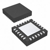
Device Information(1)
DEVICE NAME
PACKAGE
BODY SIZE
TPS53124
PW (28)
9.70 mm x 6.40 mm
TPS53124
QFN (24)
4.00 mm x 4.00 mm
(1) For all available packages, see the orderable addendum at
the end of the datasheet.
4 Simplified Schematics
Input Voltage
C9
SGND
R5
PGND
Q3
Q4
2
1
GND
VO1
7
EN2
8
VBST2
9
DRVH2
10
LL2
11
DRVL2
DRVL1 20
PGND2
PGND1 19
L2
3.3uH
3
Power PAD
TPS53124RGE
(QFN24)
15
16
VIN
VREG5
TEST2
14
V5FILT
TRIP2
13
PGND
24
DRVH1
22
LL1
21
C3
C2
0.1uF
4.7uF
Q1
L1
VO1
3.3uH
C4
12
EN1
VBST1 23
17
R6
Q2
1.05 V
C1
TRIP1
C6
4.7uF
4
VFB1
VO2
C5
0.1uF
5
VFB2
R1
6
VO2
1.8V
R2
R4
TEST1
SGND
18
R3
PGND
C7
4.7 uF
C8
1 uF
PGND
SGND
1
An IMPORTANT NOTICE at the end of this data sheet addresses availability, warranty, changes, use in safety-critical applications,
intellectual property matters and other important disclaimers. PRODUCTION DATA.
�TPS53124
SLUS825C – FEBRUARY 2008 – REVISED AUGUST 2014
www.ti.com
Table of Contents
1
2
3
4
5
6
7
Features ..................................................................
Applications ...........................................................
Description .............................................................
Simplified Schematics...........................................
Pin Configuration and Functions .........................
Specifications.........................................................
1
1
1
1
3
5
6.1
6.2
6.3
6.4
6.5
6.6
5
5
6
6
7
9
Absolute Maximum Ratings ......................................
Handling Ratings ......................................................
Recommended Operating Conditions.......................
Thermal Information ..................................................
Electrical Characteristics...........................................
Typical Characteristics ..............................................
Detailed Description ............................................ 10
7.1 Overview ................................................................. 10
7.2 Functional Block Diagram ....................................... 10
2
7.3 Feature Description................................................. 12
7.4 Device Functional Modes........................................ 13
8
Application and Implementation ........................ 14
8.1 Application Information............................................ 14
8.2 Typical Application .................................................. 14
9 Power Supply Recommendations...................... 20
10 Layout................................................................... 20
10.1 Layout Guidelines ................................................. 20
10.2 Layout Example .................................................... 20
11 Revision History .................................................. 21
12 Device and Documentation Support ................. 21
12.1 Trademarks ........................................................... 21
12.2 Electrostatic Discharge Caution ............................ 21
12.3 Glossary ................................................................ 21
13 Mechanical, Packaging, and Orderable
Information ........................................................... 21
Submit Documentation Feedback
Copyright © 2008–2014, Texas Instruments Incorporated
Product Folder Links: TPS53124
�TPS53124
www.ti.com
SLUS825C – FEBRUARY 2008 – REVISED AUGUST 2014
5 Pin Configuration and Functions
VO2
18
17
TRIP1
VIN
16
VREG5
4
5
15
V5FILT
14
13
TEST2
TRIP2
EN2
VBST2
DRVH2
LL2
DRVL2
PGND2
7
8
9
6
11
12
VFB1
GND
TEST1
VFB2
1
2
3
10
VO1
20
19
LL1
DRVL1
PGND1
VBST1
DRVH1
24
23
22
21
EN1
QFN Package
24 Pins
Top View
TSSOP Package
28 Pins
VBST1
1
28 DRVH1
NC
2
27 LL1
EN1
3
26 DRVL1
VO1
4
25 PGND1
VFB1
5
24 TRIP1
NC
6
23 VIN
GND
7
22
TEST1
8
21 V5FILT
NC
9
20 TEST2
VFB2
10
19 TRIP2
VO2
11
18 PGND2
EN2
12
17 DRVL2
NC
13
16 LL2
VBST2
14
15 DRVH2
VREG5
Submit Documentation Feedback
Copyright © 2008–2014, Texas Instruments Incorporated
Product Folder Links: TPS53124
3
�TPS53124
SLUS825C – FEBRUARY 2008 – REVISED AUGUST 2014
www.ti.com
Pin Functions
PIN
I/O
DESCRIPTION
NAME
GFN24
TSSOP28
VBST1,
VBST2
23, 8
1, 14
I
Supply input for high-side NFET driver (boost terminal). Connect capacitor from
this pin to respective LL terminals. An internal PN diode is connected between
VREG5 to each of these pins. User can add external schottky diode if forward drop
is critical to drive the NFET.
EN1, EN2
24, 7
3, 12
I
Channel 1 and Channel 2 enable pins.
VO1, VO2
1, 6
4, 11
I
Output connections to SMPS. These terminals serve ON-time adjustment, output
discharge.
VFB1,
VFB2
2, 5
5, 10
I
SMPS feedback inputs. Connect with feedback resistor divider.
GND
3
7
I
Signal ground pin.
DRVH1,
DRVH2
22, 9
28, 15
O
High-side NFET driver outputs. LL referenced floating drivers. The gate drive
voltage is defined by the voltage across VBST to LL node flying capacitor.
LL1, LL2
21, 10
27, 16
I/O
Switch-node connections for high-side drivers. Also serve as input to current
comparators.
DRVL1,
DRVL2
20, 11
26, 17
O
Synchronous NFET driver outputs. PGND referenced drivers. The gate drive
voltage is defined by VREG5 voltage.
PGND1,
PGND2
19, 12
25, 18
I/O
Ground returns for DRVL1 and DRVL2. Also serve as input of current comparators.
Connect PGND1, PGND2 and GND strongly together near the device.
TRIP1,
TRIP2
18, 13
24, 19
I
Over-current trip point set input. Connect resistor from this pin to GND to set
threshold for synchronous RDS(on) sense. Voltage across this pin and GND is
compared to voltage across PGND and LL at over current comparator.
VIN
17
23
I
Supply Input for 5-V linear regulator.
V5FILT
15
21
I
5-V supply input for the entire control circuit except the NFET drivers. Connect
capacitor (typical 1 μF) from GND to V5FILT. V5FILT is connected to VREG5 via
internal resistor.
VREG5
16
20
O
5-V power supply output. VREG5 is connected to V5FILT via internal resistor.
TEST1,
TEST2
4, 14
8, 20
I/O
Used for test only. Pin should be connected to GND
4
Submit Documentation Feedback
Copyright © 2008–2014, Texas Instruments Incorporated
Product Folder Links: TPS53124
�TPS53124
www.ti.com
SLUS825C – FEBRUARY 2008 – REVISED AUGUST 2014
6 Specifications
6.1 Absolute Maximum Ratings
over operating free-air temperature range (unless otherwise noted)
Input Voltage Range
(1)
MIN
MAX
VIN,EN1,EN2
–0.3
26
VBST1,VBST2
–0.3
32
VBST1,VBST2(wrt LLx)
–0.3
6
V5FILT,VFB1,VFB2,TRIP1,TRIP2,VO1,VO2, TEST1,TEST2
–0.3
6
–1
32
DRVH1, DRVH2
DRVH1, DRVH2 (wrt LLx)
Output Voltage Range
LL1,LL2
–0.3
6
–2
26
DRVL1,DRVL2,VREG5
–0.3
6
PGND1, PGND2
–0.3
0.3
V
V
Operating ambient temperature range, TA
–40
85
Junction Temperature Range, TJ
–40
150
(1)
UNIT
°C
Stresses beyond those listed under Absolute Maximum Ratings may cause permanent damage to the device. These are stress ratings
only, which do not imply functional operation of the device at these or any other conditions beyond those indicated under Recommended
Operating Conditions. Exposure to absolute-maximum-rated conditions for extended periods may affect device reliability.
6.2 Handling Ratings
Tstg
V(ESD)
(1)
(2)
MIN
MAX
UNIT
–55
150
°C
Human body model (HBM), per ANSI/ESDA/JEDEC JS-001, all
pins (1)
–2000
2000
Charged device model (CDM), per JEDEC specification
JESD22-C101, all pins (2)
–500
500
Storage temperature range
Electrostatic discharge
V
JEDEC document JEP155 states that 500-V HBM allows safe manufacturing with a standard ESD control process.
JEDEC document JEP157 states that 250-V CDM allows safe manufacturing with a standard ESD control process.
Submit Documentation Feedback
Copyright © 2008–2014, Texas Instruments Incorporated
Product Folder Links: TPS53124
5
�TPS53124
SLUS825C – FEBRUARY 2008 – REVISED AUGUST 2014
www.ti.com
6.3 Recommended Operating Conditions
over operating free-air temperature range (unless otherwise noted)
MIN
Supply Input Voltage Range
Input Voltage Range
Output Voltage Range
NOM
MAX
VIN
4.5
24
V5FILT
4.5
5.5
VBST1, VBST2
–0.1
30
VBST1, VBST2 (wrt LLx)
–0.1
5.5
VFB1, VFB2, VO1, VO2
–0.1
5.5
TRIP1, TRIP2
–0.1
0.3
EN1, EN2
–0.1
24
DRVH1, DRVH2
–0.1
30
VBST1, VBST2 (wrt LLx)
–0.1
5.5
1.8
24
–0.11
5.5
–0.1
0.1
LL1, LL2
DRVL1, NCDRVL2, VREG5
PGND1, PGND2
TA
Operating free-air temperature
–40
85
TJ
Operating junction temperature
–40
125
UNIT
V
V
V
°C
6.4 Thermal Information
THERMAL METRIC
(1)
TPS53124
TPS53124
TSSOP (PW)
RGE (QFN)
28 PINS
24 PINS
RθJA
Junction-to-ambient thermal resistance
79.3
35.4
RθJC(top)
Junction-to-case (top) thermal resistance
20.0
39.1
RθJB
Junction-to-board thermal resistance
37.3
13.6
ψJT
Junction-to-top characterization parameter
0.5
0.5
ψJB
Junction-to-board characterization parameter
37.8
13.6
RθJC(bot)
Junction-to-case (bottom) thermal resistance
n/a
3.8
(1)
6
UNIT
°C/W
For more information about traditional and new thermal metrics, see the IC Package Thermal Metrics application report, SPRA953.
Submit Documentation Feedback
Copyright © 2008–2014, Texas Instruments Incorporated
Product Folder Links: TPS53124
�TPS53124
www.ti.com
SLUS825C – FEBRUARY 2008 – REVISED AUGUST 2014
6.5 Electrical Characteristics
over operating free-air temperature range (unless otherwise noted)
PARAMETER
TEST CONDITIONS
MIN
TYP
MAX
450
800
UNIT
Supply Current
IIN
IVINSDN
VIN supply current
VIN current, TA = 25°C, VREG5 tied
to V5FLT, EN1 = EN2 = 5 V, VFB1
= VFB2 = 0.8 V, LL1 = LL2 = 0.5 V
VIN shutdown current
VIN current, TA = 25°C, no load,
EN1 = EN2 = 0 V
μA
10
VFB Voltage and Discharge Resistance
VBG
Bandgap initial regulation accuracy
TA = 25°C
–1%
VVFBTH
VFB threshold voltage
TA = 25°C
755
TA = -40°C to 85°C
752
IVFB
VFB input current
VFBx = 0.8 V, TA = 25°C
RDISCHG
VO discharge resistance
ENx = 0 V, VOx = 0.5 V,TA = 25°C
1%
765
775
778
mV
–0.01
±0.1
μA
40
80
Ω
5
5.2
V
VREG5 Output
VVREG5
VREG5 output voltage
TA = 25°C ,5.5 V < VIN < 24 V, 0 <
IVREG5 < 10 mA
VLN5
Line regulation
5.5 V < VIN < 24 V, IVREG5 = 10 mA
20
VLD5
Load regulation
1 mA < IVREG5 < 10 mA
40
IVREG5
Output current
VIN = 5.5 V, VREG5 = 4.0 V, TA =
25°C
170
Source, IDRVHx = -100 mA
5.5
11
Sink, IDRVHx = 100 mA
2.5
5
Source, IDRVLx = –100 mA
4
12
Sink, IDRVLx = 100 mA
2
4
4.6
mV
mA
Output: N-Channel MOSFET Gate Drivers
RDRVH
DRVH resistance
RDRVL
DRVL resistance
TD
Dead time
Ω
Ω
DRVHx-low to DRVLx-on
20
50
80
DRVLx-low to DRVHx-on
20
40
80
0.7
0.8
0.9
V
1
μA
ns
Internal BST Diode
VFBST
Forward voltage
VVREG5-VBSTx, IF = 10 mA, TA = 25°C
IVBSTLK
VBST leakage current
VBST = 29 V, LL = 24 V, TA = 25°C
0.1
ON-Time Timer Control
TON1
CH1 ON time
LL1 = 12 V, VO1 = 1.5 V
390
TON2
CH2 ON time
LL2 = 12 V, VO2 = 1.05 V
210
TON(min)
CH2 ON time
LL2 = 12 V, VO2 = 0.76 V
160
TOFF(min)
CH1/CH2 min OFF time
LL = 0.7 V TA = 25°C, VFB = 0.7 V
390
Internal SS time
Internal soft start VFB = 0.735 V
ns
Soft Start
TSS
0.85
1.2
1.4
Submit Documentation Feedback
Copyright © 2008–2014, Texas Instruments Incorporated
Product Folder Links: TPS53124
ms
7
�TPS53124
SLUS825C – FEBRUARY 2008 – REVISED AUGUST 2014
www.ti.com
Electrical Characteristics (continued)
over operating free-air temperature range (unless otherwise noted)
PARAMETER
TEST CONDITIONS
MIN
TYP
MAX
UNIT
UVLO
VUV5VFILT
V5FILT UVLO threshold
Wake up
3.7
4
4.3
Hysteresis
0.2
0.3
0.4
V
LOGIC Threshold
VENH
ENx H-level input voltage
EN 1/2
VENL
ENx L-level input voltage
EN 1/2
2
0.3
V
Current Sense
ITRIP
TRIP source current
VTRIPx = 0.1 V, TA = 25°C
TCITRIP
ITRIP temperature coefficient
On the basis of 25°C
–10
OCP compensation offset
(VTRIPx-GND - VPGNDx-LLx)
voltage,VTRIPx-GND = 60 mV, TA =
25°C
(VTRIPx-GND - VPGNDx-LLx) voltage,
VTRIPx-GND = 60 mV
–15
15
30
200
VOCL(off)
VR(trip)
Current limit threshold setting range
VTRIPx-GND voltage
8.5
10
11.5
4000
0
μA
ppm/°C
10
mV
Output Undervoltage and Overvoltage Protection
VOVP
Output OVP trip threshold
TOVPDEL
Output OVP prop delay
OVP detect
110%
115%
UVP detect
65%
70%
120%
μs
1.5
75%
VUVP
Output UVP trip threshold
TUVPDEL
Output UVP delay
17
30
40
μs
TUVPEN
Output UVP enable delay
1.2
2
2.5
ms
Hysteresis (recovery < 20 μs)
10%
Thermal Shutdown
TSDN
(1)
8
Thermal shutdown threshold
Shutdown temperature (1)
Hysteresis
(1)
150
20
°C
Ensured by design. Not production tested.
Submit Documentation Feedback
Copyright © 2008–2014, Texas Instruments Incorporated
Product Folder Links: TPS53124
�TPS53124
www.ti.com
SLUS825C – FEBRUARY 2008 – REVISED AUGUST 2014
6.6 Typical Characteristics
600
8
Shutdown Current (mA)
Supply Current (mA)
500
400
300
200
6
4
2
100
0
-50
0
50
100
Junction Temperature (qC)
0
-50
150
Figure 1. VIN Supply Current vs Junction Temperature
50
100
Junction Temperature (qC)
150
D002
Figure 2. VIN Shutdown Current vs Junction Temperature
500
Switching Frequency (kHz)
20
Source Current (mA)
0
D001
15
10
5
400
300
200
100
CH1
CH2
0
-50
0
0
50
100
Junction Temperature (qC)
150
0
5
10
15
Input Voltage (V)
D003
Figure 3. ITRIP Source Current vs Junction Temperature
20
25
D004
Figure 4. Switching Frequency vs Input Voltage
Switching Frequency (kHz)
500
400
300
200
100
CH1
CH2
0
0
1
2
Output Current (A)
3
4
D005
Figure 5. Switching Frequency vs Output Current
Submit Documentation Feedback
Copyright © 2008–2014, Texas Instruments Incorporated
Product Folder Links: TPS53124
9
�TPS53124
SLUS825C – FEBRUARY 2008 – REVISED AUGUST 2014
www.ti.com
7 Detailed Description
7.1 Overview
The TPS53124 is a dual, Adaptive on-time DCAP™ mode synchronous controller. The part enables system
designers to cost effectively complete the suite of digital TV power bus regulators with the absolute lowest
external component count and lowest standby consumption. The main control loop for the TPS53124 uses the DCAP™ mode that optimized for low ESR output capacitors such as POSCAP or SP-CAP promises fast transient
response with no external compensation. The part provides a convenient and efficient operation with conversion
voltages from 4.5 V to 24 V and output voltage from 0.76 V to 5.5 V.
7.2 Functional Block Diagram
VREG5
THOK
4 V/3.7 V
+
TSD
V50K
+
V5FILT
VO1
VO2
Switcher
Controller
FAULT
DRVL1
SDN
PGND1
VBST2
REF
DRVH2
FAULT
LL2
SDN
DRVL2
ON2
LL1
BGR
SS1
REF
ON1
DRVH1
SS2
VBST1
Switcher
Controller
PGND2
EN/SS Control
TRIP1
10
VFB1
EN1
EN2
GND
Submit Documentation Feedback
VFB2
TRIP2
Copyright © 2008–2014, Texas Instruments Incorporated
Product Folder Links: TPS53124
�TPS53124
www.ti.com
SLUS825C – FEBRUARY 2008 – REVISED AUGUST 2014
Functional Block Diagram (continued)
V5FILT
-30%
+
UV
V50K
THOK
GND
+
15%
VREG5
REF
VFBx
OV
+
+
SSx
Control Logic
PWM
VBSTx
DRVHx
10PA
1 Shot
XCON
GND
TRIPx
+
LLx
VREG5
+ OCP
LL
DRVLx
PGNDx
LLx
VOx
ENx
On/Off Time
Minimum On/Off
OVP/UVP,
Discharge Control
PGNDx
VOx
FAULT
SDN
PGNDx
Submit Documentation Feedback
Copyright © 2008–2014, Texas Instruments Incorporated
Product Folder Links: TPS53124
11
�TPS53124
SLUS825C – FEBRUARY 2008 – REVISED AUGUST 2014
www.ti.com
7.3 Feature Description
7.3.1 PWM Operation
The main control loop of the switching mode power supply (SMPS) is designed as an adaptive on-time pulse
width modulation (PWM) controller. It supports a proprietary D-CAP™ Mode. D-CAP™ Mode uses internal
compensation circuit and is suitable for low external component count configuration with appropriate amount of
ESR at the output capacitor(s). The output ripple bottom voltage is monitored at a feedback point voltage.
At the beginning of each cycle, the synchronous high-side MOSFET is turned on, or becomes ON state. This
MOSFET is turned off, or becomes OFF state, after internal one-shot timer expires. This one shot is determined
by the converter’s input voltage ,VIN, and the output voltage ,VOUT, to keep frequency fairly constant over the
input voltage range, hence it is called adaptive on-time control. The high-side MOSFET is turned on again when
feedback information indicates insufficient output voltage. Repeating operation in this manner, the controller
regulates the output voltage.
7.3.2 Low-Side Driver
The low-side driver is designed to drive high current low RDS(on) N-channel MOSFET(s). The drive capability is
represented by its internal resistance. A dead time to prevent shoot through is internally generated between highside MOSFET off to low-side MOSFET on, and low-side MOSFET off to high-side MOSFET on. 5-V bias voltage
is delivered from internal regulator VREG5 output. The instantaneous drive current is supplied by an input
capacitor connected between VREG5 and GND. The average drive current is equal to the gate charge at VGS = 5
V times switching frequency. This gate drive current as well as the high-side gate drive current times 5 V makes
the driving power which need to be dissipated from TPS53124 package.
7.3.3 High-Side Driver
The high-side driver is designed to drive high current, low RDS(on) N-channel MOSFET(s). When configured as a
floating driver, 5-V bias voltage is delivered from VREG5 supply. The average drive current is also calculated by
the gate charge at VGS = 5 V times switching frequency. The instantaneous drive current is supplied by the flying
capacitor between VBSTx and LLx pins. The drive capability is represented by its internal resistance.
7.3.4 PWM Frequency and Adaptive On-Time Control
TPS53124 employs adaptive on-time control scheme and does not have a dedicated oscillator on board.
However, the part runs with pseudo-constant frequency by feed-forwarding the input and output voltage into the
on-time one-shot timer. The on-time is controlled inverse proportional to the input voltage and proportional to the
output voltage so that the duty ratio will be kept as VOUT/VIN technically with the same cycle time.
7.3.5 Soft Start
The TPS53124 has an internal, 1.2 ms, voltage servo soft start for each channel. When the ENx pin becomes
high, an internal DAC begins ramping up the reference voltage to the PWM comparator. Smooth control of the
output voltage is maintained during start up. As TPS53124 shares one DAC with both channels, if ENx pin is set
to high while another channel is starting up, soft start is postponed until another channel soft start has
completed. If both of EN1 and EN2 are set high at a same time, both channels start up at same time.
7.3.6 Output Discharge Control
TPS53124 discharges the output when ENx is low, or the controller is turned off by the protection functions
(OVP, UVP, UVLO, and thermal shutdown). TPS53124 discharges outputs using an internal 40-Ω MOSFET
which is connected to VOx and PGNDx. The external low-side MOSFET is not turned on for the output discharge
operation to avoid the possibility of causing negative voltage at the output.
This discharge ensures that, on start, the regulated voltage always start from zero volts.
12
Submit Documentation Feedback
Copyright © 2008–2014, Texas Instruments Incorporated
Product Folder Links: TPS53124
�TPS53124
www.ti.com
SLUS825C – FEBRUARY 2008 – REVISED AUGUST 2014
Feature Description (continued)
7.3.7 Current Protection
TPS53124 has cycle-by-cycle over current limiting control. The inductor current is monitored during the ‘OFF’
state and the controller keeps the OFF state during the inductor current is larger than the over-current trip level.
In order to provide both good accuracy and cost effective solution, TPS53124 supports temperature
compensated MOSFET RDS(on) sensing. TRIPx pin should be connected to GND through the trip voltage setting
resistor, RTRIP. TRIPx terminal sources 10-μA ITRIP current at the ambient temperature and the trip level is set to
the OCL trip voltage VTRIP as below:
VTRIP ( mV ) = RTRIP ( k W ) ´10( m A )
(1)
The trip level should be in the range of 30 mV to 200 mV over all operational temperature. The inductor current is
monitored by the voltage between PGNDx pin and LLx pin. ITRIP has 4000ppm/°C temperature slope to
compensate the temperature dependency of the RDS(on). PGNDx is used as the positive current sensing node so
that PGNDx should be connected to the source terminal of the bottom MOSFET.
As the comparison is done during the OFF state, VTRIP sets valley level of the inductor current. Thus, the load
current at over-current threshold, IOCP, can be calculated as follows:
I OCP =
(V - VOUT ) ´ VOUT
VTRIP
I
V
1
+ RIPPLE = TRIP +
´ IN
2
RDS ( on )
RDS ( on ) 2 ´ L ´ f
VIN
(2)
In an over-current condition, the current to the load exceeds the current to the output capacitor; thus the output
voltage tends to fall off. Eventually, it will end up with crossing the under voltage protection threshold and
shutdown.
7.3.8 Over/Under Voltage Protection
TPS53124 monitors a resistor divided feedback voltage to detect over and under voltage. When the feedback
voltage becomes higher than 115% of the target voltage, the OVP comparator output goes high and the circuit
latches as the high-side MOSFET driver OFF and the low-side MOSFET driver ON.
When the feedback voltage becomes lower than 70% of the target voltage, the UVP comparator output goes
high and an internal UVP delay counter begins counting. After 30 μs, TPS53124 latches OFF both top and
bottom MOSFET drivers, and shut off both drivers of another channel. This function is enabled approximately 2.0
ms.
7.3.9 UVLO Protection
TPS53124 has V5FILT Under Voltage Lock Out protection (UVLO). When the V5FILT voltage is lower than
UVLO threshold voltage TPS53124 is shut off. This is non-latch protection.
7.3.10 Thermal Shutdown
TPS53124 monitors the temperature of itself. If the temperature exceeds the threshold value (typically 150°C),
the switchers will be shut off as both DRVH and DRVL at low, the output discharge function enabled. Then
TPS53124 is shut off. This is non-latch protection.
7.4 Device Functional Modes
The TPS53124 has two operating modes. The TPS53124 is in shut down mode when the EN1 and EN2 pins are
low. When the EN1 and EN2 pins is pulled high, the TPS53124 enters the normal operating mode.
Submit Documentation Feedback
Copyright © 2008–2014, Texas Instruments Incorporated
Product Folder Links: TPS53124
13
�TPS53124
SLUS825C – FEBRUARY 2008 – REVISED AUGUST 2014
www.ti.com
8 Application and Implementation
8.1 Application Information
The TPS53124 is a dual, Adaptive on-time DCAP™ mode synchronous controller. The part enables system
designers to cost effectively complete the suite of digital TV power bus regulators with the absolute lowest
external component count and lowest standby consumption. The main control loop for the TPS53124 uses the DCAP™ mode that optimized for low ESR output capacitors such as POSCAP or SP-CAP promises fast transient
response with no external compensation. The part provides a convenient and efficient operation with conversion
voltages from 4.5 V to 24 V and output voltage from 0.76 V to 5.5 V.
8.2 Typical Application
The TPS53124 is a Step-Down Controller in a realistic cost-sensitive application. Providing both a low core-type
1.05 V and I/O type 1.8 V output from a loosely regulated 12 V source. Idea applications are: Digital TV Power
Supply, Networking Home Pin and Digital Set-Top Box (STB).
Input Voltage
C9
SGND
R5
PGND
Q3
Q4
2
1
GND
VO1
7
EN2
8
VBST2
9
DRVH2
10
LL2
11
DRVL2
DRVL1 20
12
PGND2
PGND1 19
L2
3.3uH
3
Power PAD
TPS53124RGE
(QFN24)
24
DRVH1
22
LL1
21
C3
C2
0.1uF
4.7uF
Q1
L1
VO1
3.3uH
15
16
VIN
TEST2
14
VREG5
13
V5FILT
TRIP2
C4
PGND
EN1
VBST1 23
17
R6
Q2
1.05 V
C1
TRIP1
C6
4.7uF
4
VFB1
VO2
C5
0.1uF
5
VFB2
R1
6
VO2
1.8V
R2
R4
TEST1
SGND
18
R3
PGND
C7
4.7 uF
C8
1 uF
PGND
SGND
Figure 6. TPS53124 Typical Application Circuit (QFN)
14
Submit Documentation Feedback
Copyright © 2008–2014, Texas Instruments Incorporated
Product Folder Links: TPS53124
�TPS53124
www.ti.com
SLUS825C – FEBRUARY 2008 – REVISED AUGUST 2014
Typical Application (continued)
VIN
C2
0.1 PF
TPS53124
1
VSBT1
2
NC
3
DRVH1
28
LL1
27
EN1
DRVL1
26
4
VO1
PGND1
25
5
VFB1
TRP1
24
6
NC
VIN
23
C3
4.7 PF
Q1
L1
3.3 PH
VO1
R1
Q2
C1
R6
R2
C7
4.7 PF
7
GND
VREG5
C19
22
C8
1 PF
8
TEXT1
V5ALT
21
9
NC
TEXT2
20
10
VFB2
TRP2
19
11
VO2
PGND2
18
12
EN2
DRVL2
17
R5
R6
C4
Q4
13
NC
14
VSBT2
LL2
16
DRVH2
15
L2
3.3 PH
R4
C5
0.1�PF
Q3
VO2
C6
4.7 PF
VIN
Figure 7. TSSOP
Submit Documentation Feedback
Copyright © 2008–2014, Texas Instruments Incorporated
Product Folder Links: TPS53124
15
�TPS53124
SLUS825C – FEBRUARY 2008 – REVISED AUGUST 2014
www.ti.com
Typical Application (continued)
8.2.1 Design Requirements
Table 1. Design Parameters
PARAMETERS
EXAMPLE VALUES
Input voltage
12 V
Output voltage
VO1 = 1.8 V, VO2 = 1.05 V
8.2.2 Detailed Design Procedure
8.2.2.1 Choose Inductor
The inductance value is selected to provide approximately 30% peak to peak ripple current at maximum load.
Larger ripple current increases output ripple voltage, improve S/N ratio and contribute to stable operation.
Equation 3 can be used to calculate L1.
L1 =
(VIN(MAX) - VO1)´
IL1(RIPPLE) ´ ƒSW
VO 1
VIN(MAX)
=
(VIN(MAX) - VO1)´
0.3 ´ IO 1´ ƒSW
VO 1
VIN(MAX)
(3)
The inductors current ratings needs to support both the RMS (thermal) current and the Peak (saturation) current.
The RMS and peak inductor current can be estimated as follows.
IL1(RIPPLE) =
IL1(PEAK)
(VIN(MAX) - VO1)´
L1´ ƒSW
VO 1
VIN(MAX)
(4)
VTRIP
=
+ IL1(RIPPLE)
RDS(ON)
IL1(RMS) = IO 12 +
1
IL1(RIPPLE)
12
(
(5)
2
)
(6)
NOTE
The calculation above shall serve as a general reference. To further improve transient
response, the output inductance could be reduced further. This needs to be considered
along with the selection of the output capacitor.
16
Submit Documentation Feedback
Copyright © 2008–2014, Texas Instruments Incorporated
Product Folder Links: TPS53124
�TPS53124
www.ti.com
SLUS825C – FEBRUARY 2008 – REVISED AUGUST 2014
8.2.2.2 Loop Compensation and External Parts Selection
A buck converter system using D-CAP™ Mode can be simplified as below.
Voltage Divider
VIN
R1
PWM
Logic
Control
and
Driver
+
R2
REF
DRVH
LX
DRVL
IL
IC
VC
ESR
IO
CO
Figure 8. Simplifying the Modulator
The output voltage is compared with internal reference voltage after divider resistors, R1 and R2. The PWM
comparator determines the timing to turn on top MOSFET. The gain and speed of the comparator is high enough
to keep the voltage at the beginning of each on cycle (or the end of off cycle) substantially constant. The DC
output voltage may have line regulation due to ripple amplitude that slightly increases as the input voltage
increase.
For the loop stability, the 0-dB frequency, f0, defined below need to be lower than 1/3 of the switching frequency.
1
fO
f
2S u ESR u CO d SW
3
(7)
Although D-CAP™ Mode provides many advantages such as ease-of-use, minimum external components
configuration and extremely short response time, a sufficient amount of feedback signal needs to be provided by
external circuit to reduce jitter level. This is due to not employing an error amplifier in the loop. The required
signal level is approximately 10 mV at the comparing point (VFB terminal). This gives Vripples at the output node
becomes Equation 8.The output capacitor’s ESR should meet this requirement.
VOUT
VRIPPLE
u 10mV
VFBx
(8)
Submit Documentation Feedback
Copyright © 2008–2014, Texas Instruments Incorporated
Product Folder Links: TPS53124
17
�TPS53124
SLUS825C – FEBRUARY 2008 – REVISED AUGUST 2014
www.ti.com
8.2.2.3 Choose Input Capacitor
The TPS53124 requires an input decoupling capacitor and a bulk capacitor is needed depending on the
application. A minimum 10-μF high-quality ceramic capacitor is recommended for the input capacitor. The
capacitor voltage rating needs to be greater than the maximum input voltage.
8.2.2.4 Choose Bootstrap Capacitor
The TPS53124 requires a bootstrap capacitor from SW to VBST to provide the floating supply for the high-side
drivers. A minimum 0.1-μF high-quality ceramic capacitor is recommended. The voltage rating should be greater
than 10 V.
8.2.2.5 Choose VREG5 and V5FILT Capacitor
The TPS53124 requires both the VREG5 regulator and V5FILT input are bypassed. A minimum 4.7-μF highquality ceramic capacitor must be connected between the VREG5 and GND for proper operation. A minimum 1μF high-quality ceramic capacitor must be connected between the V5FILT and GND for proper operation. Both of
these capacitors’ voltage ratings should be greater than 10 V.
8.2.2.6 Choose Output Voltage Set Point Resistors
The output voltage is set with a resistor divider from the output voltage node to the VFBx pin. It is recommended
to use 1% tolerance or better resisters. Select R2 between 10 kΩ and 100 kΩ and use Equation 9 or Equation 10
to calculate R1.
æ 1 ö æ VO 1 ö
Vswinj = (VIN - VO 1´ 0.5875 )´ ç
÷´ç
÷ ´ 4975
è ƒSW ø è VIN ø
æ
ö
ç
÷
VO 1
- 1÷ ´ R2
R1 = ç
VFB(RIPPLE) + Vswinj
ç
÷
ç VFB +
÷
2
è
ø
(9)
(10)
Where
VFB(RIPPLE) = Ripple voltage at VFB
Vswinj = Ripple voltage at error comparator
8.2.2.7 Choose Over Current Set Point Resistor
æ
(VIN - VO ) VO ö
VTRIP = ç IOCL ´
÷ ´ RDS(ON)
ç
2 ´ L1´ ƒSW VIN ÷ø
è
(11)
æ
(VIN - VO ) VO ö
VTRIP = ç IOCL ´
÷ ´ RDS(ON)
ç
2 ´ L1´ ƒSW VIN ÷ø
è
(12)
Where
RDS(ON) = Low-side FET on-resistance
ITRIP(min) = TRIP pin source current (8.5 μA)
VOCL0ff = Minimum over current limit offset voltage (–20 mV)
IOCL = Over current limit
8.2.2.8 Choose Soft Start Capacitor
Soft-start time equation is as follows.
T ´I
CSS = SS SSC
VFB
18
(13)
Submit Documentation Feedback
Copyright © 2008–2014, Texas Instruments Incorporated
Product Folder Links: TPS53124
�TPS53124
www.ti.com
SLUS825C – FEBRUARY 2008 – REVISED AUGUST 2014
8.2.3 Application Curves (QFN)
1.1
1.875
VI = 5.5 V
VI = 12 V
VI = 24 V
VI = 5.5 V
VI = 12 V
VI = 24 V
1.85
Output Voltage (V)
Output Voltage (V)
1.075
1.05
1.825
1.8
1.775
1.025
1.75
1
1.725
0
1
2
Output Current (A)
3
4
0
1
D006
Figure 9. CH1 Output Voltage vs Output Current
2
Output Current (A)
3
4
D007
Figure 10. CH2 Output Voltage vs Output Current
1.875
1.1
IO = 0 A
IO = 2 A
IO = 0 A
IO = 2 A
1.85
Output Voltage (V)
Output Voltage (V)
1.075
1.05
1.825
1.8
1.775
1.025
1.75
1.725
1
0
5
10
15
Input Voltage (V)
20
25
0
5
D008
10
15
Input Voltage (V)
20
Figure 11. CH1 Output Voltage vs Input Voltage
Figure 12. CH2 Output Voltage vs Input Voltage
Figure 13. CH1 Load Step Response
Figure 14. CH2 Load Step Response
Submit Documentation Feedback
Copyright © 2008–2014, Texas Instruments Incorporated
Product Folder Links: TPS53124
25
D009
19
�TPS53124
SLUS825C – FEBRUARY 2008 – REVISED AUGUST 2014
www.ti.com
9 Power Supply Recommendations
The devices are designed to operate from an input voltage supply range between 4.5 V and 24 V. This input
supply must be well regulated. If the input supply is located more than a few inches from the TPS53124 device
additional 0.1 µF ceramic capacitance may be required in addition to the ceramic bypass capacitors, 10 µF.
10 Layout
10.1 Layout Guidelines
•
•
•
•
•
•
•
•
•
•
Keep the input switching current loop as small as possible. (VIN ≥ C3 ≥ PNGD ≥ Sync FET ≥ SW ≥ Control
FET)
Place the input capacitor (C3) close to the top switching FET. The output current loop should also be kept as
small as possible.
Keep the SW node as physically small and short as possible as to minimize parasitic capacitance and
inductance and to minimize radiated emissions. Kelvin connections should be brought from the output to the
feedback terminal (FBx) of the device.
Keep analog and non-switching components away from switching components.
Make a single point connection from the signal ground to power ground.
Do not allow switching current to flow under the device.
DRVH and DRVL line should not run close to SW node or minimize it.
GND terminals for capacitors of SSx and V5FILT and resistors of feedback and TRIPx should be connected
to SGND.
GND terminals for capacitors of VREG5 and VIN should be connected to PGND.
Signal lines should not run under/near output inductor or minimize it.
10.2 Layout Example
VIN
Q3
Q1
SW2
SW1
C3
C6
Q4
Q2
(4)
C9
(5)
(5)
L1
L2
(3) R6
C8
R3
(3)
C7
TRIP2
TEST2
V5FILT
C4, 1
16
17
18
VREG5
15
TRIP1
14
VIN
13
12 PGND2
PGND1 19
C1, 1
DRVL1 20
11 DRVL2
(QFN )
10 SW2
9 DRVH2
C5
TEST1
GND
VFB1
6
5
4
3
2
C1, 3
R2
R5
C4, 4
TO EN 1
1
R1
R4
VOUT2
C1, 2
EN1 24
VFB2
TO EN 2
C2
VBST1 23
VO2
7 EN2
C4, 3
DRVH1 22
RGE
Thermal PAD
8 VBST2
VO1
C4, 2
SW1 21
TPS53124
PGND
(3)
C1, 4
VOUT1
(1)
Top Side Component or Via
Bottom Side Component
Top Side Etch
Bottom Side Etch
Component Pads Shown in White
SGND
Figure 15. Layout Example for QFN
20
Submit Documentation Feedback
Copyright © 2008–2014, Texas Instruments Incorporated
Product Folder Links: TPS53124
�TPS53124
www.ti.com
SLUS825C – FEBRUARY 2008 – REVISED AUGUST 2014
11 Revision History
Changes from Original (February 2008) to Revision C
Page
•
Changed LSL on VREG5 from 4.8 V to 4.6 V. ...................................................................................................................... 7
•
Changed USL on RDS(on) (RDRVL / Source = –100 ma) from 8 Ω to 12 Ω. .............................................................................. 7
12 Device and Documentation Support
12.1 Trademarks
DCAP is a trademark of Texas Instruments.
12.2 Electrostatic Discharge Caution
These devices have limited built-in ESD protection. The leads should be shorted together or the device placed in conductive foam
during storage or handling to prevent electrostatic damage to the MOS gates.
12.3 Glossary
SLYZ022 — TI Glossary.
This glossary lists and explains terms, acronyms, and definitions.
13 Mechanical, Packaging, and Orderable Information
The following pages include mechanical, packaging, and orderable information. This information is the most
current data available for the designated devices. This data is subject to change without notice and revision of
this document. For browser-based versions of this data sheet, refer to the left-hand navigation.
Submit Documentation Feedback
Copyright © 2008–2014, Texas Instruments Incorporated
Product Folder Links: TPS53124
21
�PACKAGE MATERIALS INFORMATION
www.ti.com
3-Jun-2022
TAPE AND REEL INFORMATION
REEL DIMENSIONS
TAPE DIMENSIONS
K0
P1
B0 W
Reel
Diameter
Cavity
A0
B0
K0
W
P1
A0
Dimension designed to accommodate the component width
Dimension designed to accommodate the component length
Dimension designed to accommodate the component thickness
Overall width of the carrier tape
Pitch between successive cavity centers
Reel Width (W1)
QUADRANT ASSIGNMENTS FOR PIN 1 ORIENTATION IN TAPE
Sprocket Holes
Q1
Q2
Q1
Q2
Q3
Q4
Q3
Q4
User Direction of Feed
Pocket Quadrants
*All dimensions are nominal
Device
Package Package Pins
Type Drawing
SPQ
Reel
Reel
A0
Diameter Width (mm)
(mm) W1 (mm)
B0
(mm)
K0
(mm)
P1
(mm)
W
Pin1
(mm) Quadrant
TPS53124RGER
VQFN
RGE
24
3000
330.0
12.4
4.25
4.25
1.15
8.0
12.0
Q2
TPS53124RGER
VQFN
RGE
24
3000
330.0
12.4
4.25
4.25
1.15
8.0
12.0
Q2
TPS53124RGET
VQFN
RGE
24
250
180.0
12.4
4.25
4.25
1.15
8.0
12.0
Q2
TPS53124RGET
VQFN
RGE
24
250
180.0
12.4
4.25
4.25
1.15
8.0
12.0
Q2
Pack Materials-Page 1
�PACKAGE MATERIALS INFORMATION
www.ti.com
3-Jun-2022
TAPE AND REEL BOX DIMENSIONS
Width (mm)
W
L
H
*All dimensions are nominal
Device
Package Type
Package Drawing
Pins
SPQ
Length (mm)
Width (mm)
Height (mm)
TPS53124RGER
VQFN
RGE
24
3000
367.0
367.0
35.0
TPS53124RGER
VQFN
RGE
24
3000
356.0
356.0
35.0
TPS53124RGET
VQFN
RGE
24
250
210.0
185.0
35.0
TPS53124RGET
VQFN
RGE
24
250
210.0
185.0
35.0
Pack Materials-Page 2
�PACKAGE MATERIALS INFORMATION
www.ti.com
3-Jun-2022
TUBE
T - Tube
height
L - Tube length
W - Tube
width
B - Alignment groove width
*All dimensions are nominal
Device
Package Name
Package Type
Pins
SPQ
L (mm)
W (mm)
T (µm)
B (mm)
TPS53124PW
PW
TSSOP
28
50
530
10.2
3600
3.5
Pack Materials-Page 3
�GENERIC PACKAGE VIEW
RGE 24
VQFN - 1 mm max height
PLASTIC QUAD FLATPACK - NO LEAD
Images above are just a representation of the package family, actual package may vary.
Refer to the product data sheet for package details.
4204104/H
�PACKAGE OUTLINE
RGE0024B
VQFN - 1 mm max height
SCALE 3.000
PLASTIC QUAD FLATPACK - NO LEAD
4.1
3.9
A
B
0.5
0.3
PIN 1 INDEX AREA
4.1
3.9
0.3
0.2
DETAIL
OPTIONAL TERMINAL
TYPICAL
C
1 MAX
SEATING PLANE
0.05
0.00
0.08 C
2X 2.5
(0.2) TYP
2.45 0.1
7
SEE TERMINAL
DETAIL
12
EXPOSED
THERMAL PAD
13
6
2X
2.5
SYMM
25
18
1
20X 0.5
24
PIN 1 ID
(OPTIONAL)
0.3
0.2
0.1
C A B
0.05
24X
19
SYMM
24X
0.5
0.3
4219013/A 05/2017
NOTES:
1. All linear dimensions are in millimeters. Any dimensions in parenthesis are for reference only. Dimensioning and tolerancing
per ASME Y14.5M.
2. This drawing is subject to change without notice.
3. The package thermal pad must be soldered to the printed circuit board for thermal and mechanical performance.
www.ti.com
�EXAMPLE BOARD LAYOUT
RGE0024B
VQFN - 1 mm max height
PLASTIC QUAD FLATPACK - NO LEAD
( 2.45)
SYMM
24
19
24X (0.6)
1
18
24X (0.25)
(R0.05)
TYP
25
SYMM
(3.8)
20X (0.5)
13
6
( 0.2) TYP
VIA
12
7
(0.975) TYP
(3.8)
LAND PATTERN EXAMPLE
EXPOSED METAL SHOWN
SCALE:15X
0.07 MIN
ALL AROUND
0.07 MAX
ALL AROUND
SOLDER MASK
OPENING
METAL
EXPOSED
METAL
SOLDER MASK
OPENING
EXPOSED
METAL
NON SOLDER MASK
DEFINED
(PREFERRED)
METAL UNDER
SOLDER MASK
SOLDER MASK
DEFINED
SOLDER MASK DETAILS
4219013/A 05/2017
NOTES: (continued)
4. This package is designed to be soldered to a thermal pad on the board. For more information, see Texas Instruments literature
number SLUA271 (www.ti.com/lit/slua271).
5. Vias are optional depending on application, refer to device data sheet. If any vias are implemented, refer to their locations shown
on this view. It is recommended that vias under paste be filled, plugged or tented.
www.ti.com
�EXAMPLE STENCIL DESIGN
RGE0024B
VQFN - 1 mm max height
PLASTIC QUAD FLATPACK - NO LEAD
4X ( 1.08)
(0.64) TYP
24
19
24X (0.6)
1
25
18
24X (0.25)
(R0.05) TYP
(0.64)
TYP
SYMM
(3.8)
20X (0.5)
13
6
METAL
TYP
12
7
SYMM
(3.8)
SOLDER PASTE EXAMPLE
BASED ON 0.125 mm THICK STENCIL
EXPOSED PAD 25
78% PRINTED SOLDER COVERAGE BY AREA UNDER PACKAGE
SCALE:20X
4219013/A 05/2017
NOTES: (continued)
6. Laser cutting apertures with trapezoidal walls and rounded corners may offer better paste release. IPC-7525 may have alternate
design recommendations.
www.ti.com
���IMPORTANT NOTICE AND DISCLAIMER
TI PROVIDES TECHNICAL AND RELIABILITY DATA (INCLUDING DATA SHEETS), DESIGN RESOURCES (INCLUDING REFERENCE
DESIGNS), APPLICATION OR OTHER DESIGN ADVICE, WEB TOOLS, SAFETY INFORMATION, AND OTHER RESOURCES “AS IS”
AND WITH ALL FAULTS, AND DISCLAIMS ALL WARRANTIES, EXPRESS AND IMPLIED, INCLUDING WITHOUT LIMITATION ANY
IMPLIED WARRANTIES OF MERCHANTABILITY, FITNESS FOR A PARTICULAR PURPOSE OR NON-INFRINGEMENT OF THIRD
PARTY INTELLECTUAL PROPERTY RIGHTS.
These resources are intended for skilled developers designing with TI products. You are solely responsible for (1) selecting the appropriate
TI products for your application, (2) designing, validating and testing your application, and (3) ensuring your application meets applicable
standards, and any other safety, security, regulatory or other requirements.
These resources are subject to change without notice. TI grants you permission to use these resources only for development of an
application that uses the TI products described in the resource. Other reproduction and display of these resources is prohibited. No license
is granted to any other TI intellectual property right or to any third party intellectual property right. TI disclaims responsibility for, and you
will fully indemnify TI and its representatives against, any claims, damages, costs, losses, and liabilities arising out of your use of these
resources.
TI’s products are provided subject to TI’s Terms of Sale or other applicable terms available either on ti.com or provided in conjunction with
such TI products. TI’s provision of these resources does not expand or otherwise alter TI’s applicable warranties or warranty disclaimers for
TI products.
TI objects to and rejects any additional or different terms you may have proposed. IMPORTANT NOTICE
Mailing Address: Texas Instruments, Post Office Box 655303, Dallas, Texas 75265
Copyright © 2022, Texas Instruments Incorporated
�


 工商网监
湘ICP备2023018690号
工商网监
湘ICP备2023018690号
