Sample &
Buy
Product
Folder
Support &
Community
Tools &
Software
Technical
Documents
TPS53310
SLUSA68A – DECEMBER 2010 – REVISED OCTOBER 2016
TPS53310 3-A Step-Down Regulator With Integrated Switcher
1 Features
3 Description
•
•
•
•
•
The TPS53310 provides a fully integrated 3-V to 5-V
VIN integrated synchronous FET converter solution
with 16 total components, in 200 mm2 of PCB area.
Due to the low RDS(on) and TI's proprietary
SmoothPWM™ Skip mode of operation, it enables
95.5% peak efficiency, and over 90% efficiency at
loads as light as 100 mA. It requires only two 22-µF
ceramic output capacitors for a power dense 3-A
solution.
1
•
•
•
•
•
•
•
•
•
•
•
•
>95% Maximum Efficiency
Continuous 3-A Output Current
Hiccup Overcurrent Protection
Supports All MLCC Output Capacitor
SmoothPWM™ Auto-Skip Eco-mode™ for LightLoad Efficiency
Voltage Mode Control
Supports Master-Slave Interleaved Operation
Synchronization up to ±20% of Nominal
Frequency
Conversion Voltage Range Between 2.9 V and
6V
Soft-Stop Output Discharge During Disable
Adjustable Output Voltage Ranging Between
0.6 V and 0.84 V × VIN
Undervoltage, Overvoltage and Overtemperature
Protection
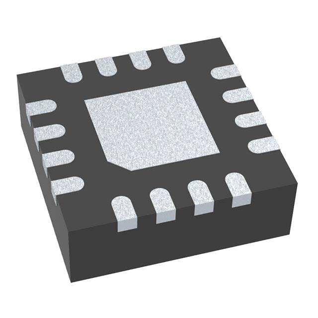
Small 3 mm × 3 mm, 16-Pin VQFN Package
Open-Drain Power Good Indication
Internal Boot Strap Switch
Low RDS(on), 24 mΩ with 3.3-V Input and 19-mΩ
with 5-V Input
Supports Pre-bias Start Up
The TPS53310 features a 1.1-MHz switching
frequency, SKIP mode operation support, pre-bias
startup, internal softstart, output soft discharge,
internal VBST switch, power good, EN/input UVLO,
overcurrent,
overvoltage,
undervoltage
and
overtemperature protections and all ceramic output
capacitor support. It supports supply voltage from
2.9 V to 3.5 V and conversion voltage from 2.9 V to
6 V, and output voltage is adjustable from 0.6 V to
0.84 V × VIN.
The TPS53310 is available in the 3 mm × 3 mm,
16-pin VQFN package (Green RoHs compliant and
Pb free) and operates between –40°C and 85°C.
Device Information(1)
PART NUMBER
TPS53310
PACKAGE
VQFN (16)
BODY SIZE (NOM)
3.00 mm × 3.00 mm
(1) For all available packages, see the orderable addendum at
the end of the data sheet.
2 Applications
•
•
5-V Step-Down Rail
3.3-V Step-Down Rail
Typical Application Circuit
Output All MLCCs
VIN
2.9 V to 6 V
VDD
2.9 V to 3.5 V
13
14
5
VIN
VIN
6
7
CBST
SW SW SW
12 VDD
VBST
4
PGD
3
VIN
11 AGND
SYNC
2
SYNC
EN
1
EN
8
PS
TPS53310
PGD
FB 10
PGND PGND
15
Pad
COMP
9
16
UDG-10210
Copyright © 2016, Texas Instruments Incorporated
1
An IMPORTANT NOTICE at the end of this data sheet addresses availability, warranty, changes, use in safety-critical applications,
intellectual property matters and other important disclaimers. PRODUCTION DATA.
�TPS53310
SLUSA68A – DECEMBER 2010 – REVISED OCTOBER 2016
www.ti.com
Table of Contents
1
2
3
4
5
6
7
Features ..................................................................
Applications ...........................................................
Description .............................................................
Revision History.....................................................
Pin Configuration and Functions .........................
Specifications.........................................................
1
1
1
2
3
4
6.1
6.2
6.3
6.4
6.5
6.6
4
4
4
5
5
7
Absolute Maximum Ratings ......................................
ESD Ratings..............................................................
Recommended Operating Conditions.......................
Thermal Information ..................................................
Electrical Characteristics...........................................
Typical Characteristics ..............................................
Detailed Description .............................................. 9
7.1
7.2
7.3
7.4
Overview ................................................................... 9
Functional Block Diagram ......................................... 9
Feature Description................................................... 9
Device Functional Modes........................................ 10
7.5 Programming........................................................... 11
8
Application and Implementation ........................ 12
8.1 Application Information............................................ 12
8.2 Typical Application .................................................. 12
9 Power Supply Recommendations...................... 19
10 Layout................................................................... 19
10.1 Layout Guidelines ................................................. 19
10.2 Layout Example .................................................... 19
11 Device and Documentation Support ................. 20
11.1
11.2
11.3
11.4
11.5
11.6
Documentation Support ........................................
Receiving Notification of Documentation Updates
Community Resources..........................................
Trademarks ...........................................................
Electrostatic Discharge Caution ............................
Glossary ................................................................
20
20
20
20
20
20
12 Mechanical, Packaging, and Orderable
Information ........................................................... 20
4 Revision History
NOTE: Page numbers for previous revisions may differ from page numbers in the current version.
Changes from Original (December 2010) to Revision A
Page
•
Added ESD Ratings table, Feature Description section, Device Functional Modes, Application and Implementation
section, Power Supply Recommendations section, Layout section, Device and Documentation Support section, and
Mechanical, Packaging, and Orderable Information section .................................................................................................. 1
•
Deleted Ordering Information table; see POA at the end of the data sheet........................................................................... 1
•
Deleted Lead temperature from Absolute Maximum Ratings table........................................................................................ 4
•
Deleted Package Dissipation Ratings table............................................................................................................................ 5
•
Added Thermal Information table ........................................................................................................................................... 5
•
Changed value of R2 component in Typical 3.3-V Input Application Circuit Diagram From: 4.02 kΩ To: 2.67 kΩ ............. 12
•
Changed value of VOUT component on TPS53310 Master in Master and Slave Configuration Schematic From: 1.2 V
To: 1.5 V ............................................................................................................................................................................... 16
•
Changed value of R2 component on TPS53310 Master in Master and Slave Configuration Schematic From: 4.02 kΩ
To: 2.67 kΩ ........................................................................................................................................................................... 16
•
Changed value of VOUT component on TPS53310 Slave in Master and Slave Configuration Schematic From: 1.5 V
To: 1.2 V ............................................................................................................................................................................... 16
•
Changed value of R2 component on TPS53310 Slave in Master and Slave Configuration Schematic From: 2.67 kΩ
To: 4.02 kΩ ........................................................................................................................................................................... 16
2
Submit Documentation Feedback
Copyright © 2010–2016, Texas Instruments Incorporated
Product Folder Links: TPS53310
�TPS53310
www.ti.com
SLUSA68A – DECEMBER 2010 – REVISED OCTOBER 2016
5 Pin Configuration and Functions
VBST
VIN
VIN
PGD
14
13
2
PGND
SYNC
15
1
PGND
EN
16
RGT Package
16-Pin VQFN
Top View
12
VDD
6
7
8
SW
PS
COMP
SW
9
5
4
SW
AGND
3
11
Thermal
Pad
10
FB
Not to scale
Pin Functions
PIN
NO.
NAME
TYPE (1)
DESCRIPTION
1
EN
I
Enable. Internally pulled up to VDD with a 1.35-MΩ resistor.
2
SYNC
B
Synchronization signal for input interleaving. Master SYNC pin sends out 180° out-of-phase signal to
slave SYNC. SYNC frequency must be within ±20% of slave nominal frequency.
3
PGD
O
Power good output flag; Open drain output. Pull up to an external rail through a resistor.
4
VBST
P
Supply input for high-side MOSFET (bootstrap terminal); Connect capacitor from this pin to SW
terminal.
5
SW
B
Output inductor connection to integrated power devices
6
SW
B
Output inductor connection to integrated power devices
7
SW
B
Output inductor connection to integrated power devices
8
PS
I
Mode configuration pin (with 10 µA current):
Connecting to ground: Forced CCM slave
Pulled high or floating (internal pulled high): Forced CCM master
Connect with 24.3 kΩ to GND: DE slave
Connect with 57.6 kΩ to GND: HEF mode
Connect with 105 kΩ to GND: reserved mode
Connect with 174 kΩ to GND: DE master
9
COMP
O
Error amplifier compensation terminal; Type III compensation method is recommended for stability.
10
FB
I
Voltage feedback (also used for OVP, UVP and PGD determination)
11
AGND
G
Device analog ground terminal
12
VDD
P
Input bias supply for analog functions
13
VIN
P
Gate driver supply and power conversion voltage
14
VIN
P
Gate driver supply and power conversion voltage
15
PGND
P
Power ground terminal
16
PGND
P
Power ground terminal
(1)
B = Bidirectional, G = Ground, I = Input, O = Output, P = Supply
Submit Documentation Feedback
Copyright © 2010–2016, Texas Instruments Incorporated
Product Folder Links: TPS53310
3
�TPS53310
SLUSA68A – DECEMBER 2010 – REVISED OCTOBER 2016
www.ti.com
6 Specifications
6.1 Absolute Maximum Ratings
over operating free-air temperature range (unless otherwise noted) (1)
Input voltage
MIN
MAX
VIN, EN
–0.3
7
VBST
–0.3
17
VBST(with respect to SW)
–0.3
7
FB, PS, VDD
–0.3
3.7
DC
UNIT
V
–0.3
7
–3
10
PGD
–0.3
7
COMP, SYNC
–0.3
3.7
PGND
–0.3
0.3
Junction temperature, TJ
–40
150
°C
Ambient temperature, TA
–40
85
°C
Storage temperature, Tstg
–55
150
°C
SW
Output voltage
(1)
Pulse < 20 ns, E = 5 μJ
V
Stresses beyond those listed under Absolute Maximum Ratings may cause permanent damage to the device. These are stress ratings
only, which do not imply functional operation of the device at these or any other conditions beyond those indicated under Recommended
Operating Conditions. Exposure to absolute-maximum-rated conditions for extended periods may affect device reliability.
6.2 ESD Ratings
VALUE
V(ESD)
(1)
(2)
Electrostatic discharge
Human-body model (HBM), per ANSI/ESDA/JEDEC JS-001
(1)
UNIT
±2000
Charged-device model (CDM), per JEDEC specification JESD22-C101 (2)
V
±500
JEDEC document JEP155 states that 500-V HBM allows safe manufacturing with a standard ESD control process.
JEDEC document JEP157 states that 250-V CDM allows safe manufacturing with a standard ESD control process.
6.3 Recommended Operating Conditions
MIN
Input voltage
TJ
4
MAX
3.3
3.5
VIN
2.9
VDD
2.9
VBST
–0.1
13.5
VBST (with respect to SW)
–0.1
6
EN
–0.1
6
FB, PS
–0.1
3.5
–1
6.5
SW
Output voltage
NOM
6
PGD
–0.1
6
COMP, SYNC
–0.1
3.5
PGND
–0.1
0.1
–40
125
Junction temperature
Submit Documentation Feedback
UNIT
V
V
°C
Copyright © 2010–2016, Texas Instruments Incorporated
Product Folder Links: TPS53310
�TPS53310
www.ti.com
SLUSA68A – DECEMBER 2010 – REVISED OCTOBER 2016
6.4 Thermal Information
TPS53310
THERMAL METRIC (1)
RGT (VQFN)
UNIT
16 PINS
RθJA
Junction-to-ambient thermal resistance
42.8
°C/W
RθJC(top)
Junction-to-case (top) thermal resistance
51.3
°C/W
RθJB
Junction-to-board thermal resistance
16
°C/W
ψJT
Junction-to-top characterization parameter
0.7
°C/W
ψJB
Junction-to-board characterization parameter
16
°C/W
RθJC(bot)
Junction-to-case (bottom) thermal resistance
4.4
°C/W
(1)
For more information about traditional and new thermal metrics, see the Semiconductor and IC Package Thermal Metrics application
report.
6.5 Electrical Characteristics
over recommended free-air temperature range, VIN = 3.3 V, VVDD = 3.3 V, PGND = GND (Unless otherwise noted).
PARAMETER
CONDITIONS
MIN
TYP
MAX
UNIT
SUPPLY: VOLTAGE, CURRENTS, AND UVLO
VIN
VIN supply voltage
Nominal input voltage range
2.9
IVINSDN
VIN shutdown current
EN = LO
VUVLO
VIN UVLO threshold
Ramp up, EN = HI
2.8
V
VUVLOHYS
VIN UVLO hysteresis
VIN UVLO Hysteresis
130
mV
VDD
Internal circuitry supply voltage
Nominal 3.3-V input voltage range
IDDSDN
VDD shut down current
EN = LO
IDD
Standby current
VDDUVLO
3.3-V UVLO threshold
VDDUVLOHYS
3.3-V UVLO hysteresis
2.9
6
V
3
µA
3.3
3.5
V
5
µA
EN = HI, no switching
2.2
3.5
mA
Ramp up, EN = HI
2.8
V
75
mV
0.6
V
VOLTAGE FEEDBACK LOOP: VREF AND ERROR AMPLIFIER
VVREF
VREF
TOLVREF
VREF Tolerance
UGBW (1)
Unity gain bandwidth
14
MHz
AOL (1)
Open loop gain
80
dB
IFBINT
IEAMAX
(1)
SR (1)
Internal precision reference voltage
0°C ≤ TA ≤ 85°C
–40°C ≤ TA ≤ 85°C
FB input leakage current
Sourced from FB pin
Output sinking and sourcing
current
CCOMP = 20 pF
–1%
1%
–1.25%
1.25%
30
Slew rate
nA
5
mA
5
V/µs
OCP: OVERCURRENT AND ZERO CROSSING
IOCPL
Overcurrent limit on upper FET
When IOUT exceeds this threshold for 4
consecutive cycles. VIN = 3.3 V,
VOUT = 1.5 V with 1-µH inductor, TA = 25°C
4.2
4.5
4.8
A
IOCPH
One time overcurrent latch off
on the lower FET
Immediately shut down when sensed current
reach this value. VIN = 3.3 V,
VOUT = 1.5 V with 1-µH inductor, TA = 25°C
4.8
5.1
5.5
A
VZXOFF (1)
Zero crossing comparator
internal offset
PGND – SW, SKIP mode
–4.5
–3
–1.5
mV
tHICCUP
Hiccup time interval
12.5
14.5
16.5
ms
PROTECTION: OVP, UVP, PGD, AND INTERNAL THERMAL SHUTDOWN
VOVP
Overvoltage protection
threshold voltage
Measured at FB wrt. VREF
114%
117%
120%
VUVP
Undervoltage protection
threshold voltage
Measured at FB wrt. VREF
80%
83%
86%
(1)
Ensured by design. Not production tested.
Submit Documentation Feedback
Copyright © 2010–2016, Texas Instruments Incorporated
Product Folder Links: TPS53310
5
�TPS53310
SLUSA68A – DECEMBER 2010 – REVISED OCTOBER 2016
www.ti.com
Electrical Characteristics (continued)
over recommended free-air temperature range, VIN = 3.3 V, VVDD = 3.3 V, PGND = GND (Unless otherwise noted).
PARAMETER
CONDITIONS
MIN
TYP
MAX
VPGDL
PGD low threshold
Measured at FB wrt. VREF
80%
83%
86%
VPGDU
PGD upper threshold
Measured at FB wrt. VREF
114%
117%
120%
VINMINPG
Minimum VIN voltage for valid
PGD at start up
Measured at VIN with 1-mA (or 2-mA) sink
current on PGD pin at start up
THSD (1)
Thermal shutdown
Latch off controller, attempt soft-stop
THSDHYS (1)
Thermal shutdown hysteresis
Controller restarts after temperature has dropped
1
130
140
UNIT
V
150
40
°C
°C
LOGIC PINS: I/O VOLTAGE AND CURRENT
VPGPD
PGD pull down voltage
Pull-down voltage with 4-mA sink current
IPGLK
PGD leakage current
Hi-Z leakage current, apply 3.3-V in off state
RENPU
Enable pull up resistor
VENH
EN logic high threshold
VENHYS
EN hysteresis
–2
PS mode threshold voltage
0.4
V
0
2
µA
1.35
1.1
Level 1 to level 2 (2)
PSTHS
0.2
MΩ
1.18
1.3
V
0.18
0.24
V
0.12
Level 2 to level 3
0.4
Level 3 to level 4
0.8
Level 4 to level 5
1.4
Level 5 to level 6
2.2
IPS
PS source
10-µA pull-up current when enabled.
8
fSYNCSL
Slave SYNC frequency range
Versus nominal switching frequency
–20%
PWSYNC
SYNC low pulse width
ISYNC
SYNC pin sink current
VSYNCTHS (1)
SYNC threshold
VSYNCHYS (1)
SYNC hysteresis
10
V
12
µA
20%
110
ns
TA = 25°C
10
µA
Falling edge
1.0
V
0.5
V
BOOT STRAP: VOLTAGE AND LEAKAGE CURRENT
IVBSTLK
VBST leakage current
VIN = 3.3 V, VVBST = 6.6 V, TA = 25°C
1
µA
TIMERS: SS, FREQUENCY, RAMP, ON TIME AND I/O TIMING
tSS_1
Delay after EN asserting
EN = 'HI', master or HEF mode
0.2
ms
tSS_2
Delay after EN asserting
EN = 'HI', slave waiting time
0.5
ms
tSS_3
Soft-start ramp-up time
Rising from VSS = 0 V to VSS = 0.6 V
0.4
ms
tPGDENDLY
PGD startup delay time
Rising from VSS = 0 V to VSS = 0.6 V,
from VSS reaching 0.6 V to VPGD going high
0.4
ms
tOVPDLY
Overvoltage protection delay
time
Time from FB out of +20% of VREF to OVP fault
tUVPDLY
Undervoltage protection delay
time
Time from FB out of -20% of VREF to UVP fault
fSW
Switching frequency control
Forced CCM mode
Ramp amplitude (1)
2.9 V < VIN < 6 V
tMIN(off)
Minimum OFF time
DMAX
Maximum duty cycle
RSFTSTP
Soft-discharge transistor
resistance
(2)
6
1.0
1.7
2.5
11
0.99
1.1
µs
1.21
VIN / 4
100
140
HEF mode
175
250
84%
89%
HEF mode, fSW = 1.1 MHz, 0°C ≤ TA ≤ 85°C
75%
81%
VEN = Low, VIN = 3.3 V, VOUT = 0.5 V
60
MHz
V
FCCM mode or DE mode
FCCM mode and DE mode, fSW = 1.1 MHz, 0°C
≤ TA ≤ 85°C
µs
ns
Ω
See PS pin description for levels.
Submit Documentation Feedback
Copyright © 2010–2016, Texas Instruments Incorporated
Product Folder Links: TPS53310
�TPS53310
www.ti.com
SLUSA68A – DECEMBER 2010 – REVISED OCTOBER 2016
6.6 Typical Characteristics
Inductor IN06142 (1 µH, 5.4 mΩ) is used
h – Efficiency – %
96
96
VOUT = 2.5 V
VOUT = 2.5 V
94
94
92
92
90
90
88
88
VOUT = 1.2 V
VOUT = 1.2 V
86
86
VOUT = 1.5 V
VOUT = 1.5 V
VOUT = 1.8 V
VOUT = 1.8 V
84
84
Skip Mode
VIN = 3.3 V
82
FCCM Mode
VIN = 3.3 V
82
80
80
0
0.5
1.0
1.5
2.0
2.5
3.0
0
0.5
IOUT – Output Current – A
Figure 1. Efficiency vs Output Current,
Skip Mode, VIN = 3.3 V
1.5
2.0
2.5
3.0
Figure 2. Efficiency vs Output Current,
FCCM, VIN = 3.3 V
96
96
VOUT = 2.5 V
VOUT = 2.5 V
94
94
92
92
90
88
VOUT = 1.5 V
86
VOUT = 1.8 V
VOUT = 1.2 V
h – Efficiency – %
h – Efficiency – %
1.0
IOUT – Output Current – A
84
90
88
VOUT = 1.5 V
86
VOUT = 1.8 V
VOUT = 1.2 V
84
Skip Mode
VIN = 5 V
82
FCCM Mode
VIN = 5 V
82
80
80
0
0.5
1.0
1.5
2.0
2.5
3.0
0
0.5
1.0
1.5
2.0
2.5
3.0
IOUT – Output Current – A
IOUT – Output Current – A
Figure 3. Efficiency vs Output Current,
Skip Mode, VIN = 5 V
Figure 4. Efficiency vs Output Current,
FCCM, VIN = 5 V
0.5
0.620
0.615
VFB – Feedback Voltage – V
0.3
Output Voltage Change (%)
0.610
0.605
0.600
0.595
0.590
0.1
– 0.1
– 0.3
VIN = 5.0 V
VIN = 3.3 V
0.585
0.580
–40 –25 –10
– 0.5
5
20
35
50
65
80
0
95 110 125
0.5
1.0
1.5
2.0
2.5
3.0
TA – Ambient Temperature – °C
Output Current (A)
Figure 5. Feedback Voltage vs Ambient Temperature
Figure 6. Output Voltage Change vs Output Current
Submit Documentation Feedback
Copyright © 2010–2016, Texas Instruments Incorporated
Product Folder Links: TPS53310
7
�TPS53310
SLUSA68A – DECEMBER 2010 – REVISED OCTOBER 2016
www.ti.com
Typical Characteristics (continued)
Inductor IN06142 (1 µH, 5.4 mΩ) is used
10 k
10 k
Mode
FCCM
HEF
DE
1000
Frequency (kHz)
Frequency (kHz)
Mode
FCCM
HEF
DE
100
1000
100
VIN = 3.3 V
10
0.01
0.1
1.0
VIN = 5.0 V
10
0.01
10
0.1
1.0
10
Output Current (A)
Output Current (A)
Figure 7. Frequency vs Output Current
at VIN = 3.3 V
Figure 8. Frequency vs Output Current
at VIN = 5 V
HEF Mode
VIN = 3.3 V
IOUT = 0 A
HEF Mode
VIN = 3.3 V
IOUT = 0 A
EN (5 V/div)
EN (5 V/div)
0.5 V pre-biased
VOUT (1 V/div)
VOUT (1 V/div)
PGD (5 V/div)
PGD (5 V/div)
t – Time – 200 ms/div
t – Time – 200 ms/div
Figure 9. Normal Start Up Waveform
Figure 10. Pre-Bias Start Up Waveform
90
80
EN (5 V/div)
HEF Mode
VIN = 3.3 V
IOUT = 0 A
Temperature (C)
VOUT (1 V/div)
60
50
40
PGD (5 V/div)
30
20
0.0
VIN = 3.3 V @
VOUT = 0.6 V
VOUT = 1.2 V
VOUT = 1.8 V
VOUT = 2.5 V
0.5
VIN = 5 V @
VOUT = 0.6 V
VOUT = 1.2 V
VOUT = 1.8 V
VOUT = 2.5 V
VOUT = 3.3 V
1.0
1.5
2.0
2.5
3.0
Output Current (A)
t – Time – 4 ms/div
Figure 11. Soft-Stop Waveform
8
No Air Flow
70
Submit Documentation Feedback
Figure 12. Safe Operating Area
Copyright © 2010–2016, Texas Instruments Incorporated
Product Folder Links: TPS53310
�TPS53310
www.ti.com
SLUSA68A – DECEMBER 2010 – REVISED OCTOBER 2016
7 Detailed Description
7.1 Overview
The TPS53310 is a high-efficiency switching regulator with two integrated N-channel MOSFETs and is capable
of delivering up to 3 A of load current. The TPS53310 provides output voltage between 0.6 V and 0.84 × VIN from
2.9 V to 6 V wide input voltage range.
This device employs five operation modes to fit various application requirements. The master and slave mode
enables a two-phase interleaved operation to reduce input ripple. The skip mode operation provides reduced
power loss and increases the efficiency at light load. The unique, patented PWM modulator enables smooth light
load to heavy load transition while maintaining fast load transient.
7.2 Functional Block Diagram
0.6 V–17%
UV/OV
Threshold
Generation
0.6 V
+
0.6 V+17%
VIN
14
13
+
OV
Control
Logic
HDRV
PWM
+
COMP
9
E/A
0.6 V
+
Ramp
4
VBST
5
SW
6
SW
7
SW
VIN UVLO
UV
FB 10
VIN
+
XCON
PWM
LL One-Shot
Overtemp
VOUT Discharge
SS
LDRV
15 PGND
16 PGND
OSC
Enable
Control
OCP Logic
Mode
Scanner
VDD UVLO
12 VDD
2
1
8
3
11
SYNC
EN
PS
PGD
AGND
TPS53310
UDG-10028
Copyright © 2016, Texas Instruments Incorporated
7.3 Feature Description
7.3.1 Soft Start
The soft-start function reduces the inrush current during the start up sequence. A slow-rising reference voltage is
generated by the soft-start circuitry and sent to the input of the error amplifier. When the soft-start ramp voltage
is less than 600 mV, the error amplifier uses this ramp voltage as the reference. When the ramp voltage reaches
600 mV, the error amplifier switches to a fixed 600-mV reference. The typical soft-start time is 400 µs.
7.3.2 Power Good
The TPS53310 monitors the voltage on the FB pin. If the FB voltage is between 83% and 117% of the reference
voltage, the power good signal remains high. If the FB voltage falls outside of these limits, the internal open drain
output pulls the power good pin (PGD) low.
Submit Documentation Feedback
Copyright © 2010–2016, Texas Instruments Incorporated
Product Folder Links: TPS53310
9
�TPS53310
SLUSA68A – DECEMBER 2010 – REVISED OCTOBER 2016
www.ti.com
Feature Description (continued)
During start-up, VIN must be higher than 1-V to have valid power good logic, and the power good signal is
delayed for 400 µs after the FB voltage falls to within the power good limits. There is also 10-µs delay during the
shut down sequence.
7.3.3 Undervoltage Lockout (UVLO) Function
The TPS53310 provides undervoltage lockout (UVLO) protection for both power input (VIN) and bias input (VDD)
voltage. If either of them is lower than the UVLO threshold voltage minus the hysteresis, the device shuts off.
When the voltage rises above the threshold voltage, the device restarts. The typical UVLO rising threshold is 2.8
V for both VIN and VVDD. A hysteresis voltage of 130 mV for VIN and 75 mV for VVDD is also provided to prevent
glitch.
7.3.4 Overcurrent Protection
The TPS53310 continuously monitors the current flowing through the high-side and the low-side MOSFETs. If
the current through the high-side FET exceeds 4.5 A, the high-side FET turns off and the low-side FET turns on
until the next PWM cycle. An overcurrent (OC) counter starts to increment each occurrence of an overcurrent
event. The converter shuts down immediately when the OC counter reaches four. The OC counter resets if the
detected current is less 4.5 A after an OC event.
Another set of overcurrent circuitry monitors the current flowing through low-side FET. If the current through the
low-side FET exceeds 5.1 A, the overcurrent protection is enabled and immediately turns off both the high-side
and the low-side FETs and shuts down the converter . The device is fully protected against overcurrent during
both on-time and off-time.
The device attempts to restart after a hiccup delay (14.5-ms typical). If the overcurrent condition is cleared before
restart, the device starts up normally. See the TPS53311 datasheet, TPS53311 3-A Step-Down Regulator With
Integrated Switcher (SLUSA41), for information on latch-off overcurrent protection.
7.3.5 Overvoltage Protection
The TPS53310 monitors the voltage divided feedback voltage to detect overvoltage and undervoltage conditions.
When the feedback voltage is greater than 117% of the reference, the high-side MOSFET turns off and the lowside MOSFET turns on. The output voltage then drops until it reaches the undervoltage threshold. At that point
the low-side MOSFET turns off and the device enters a high-impedance state.
7.3.6 Undervoltage Protection
When the feedback voltage is lower than 83% of the reference voltage, the undervoltage protection timer starts.
If the feedback voltage remains lower than the undervoltage threshold voltage after 10 μs, the device turns off
both the high-side and the low-side MOSFETs and goes into a high-impedance state. The device attempts to
restart after a hiccup delay (14.5 ms typical).
7.3.7 Overtemperature Protection
The TPS53310 continuously monitors the die temperature. If the die temperature exceeds the threshold value
(140˚C typical), the device shuts off. When the device temperature falls to 40˚C below the overtemperature
threshold, it restarts and returns to normal operation.
7.3.8 Output Discharge
When the enable pin is low, the TPS53310 discharges the output capacitors through an internal MOSFET switch
between SW and PGND while high-side and low-side MOSFETs remain off. The typical discharge switch-on
resistance is 60 Ω. This function is disabled when VIN is less than 1 V.
7.4 Device Functional Modes
7.4.1 Operation Mode
The TPS53310 offers five operation modes determined by the PS pin connections listed in Table 1.
10
Submit Documentation Feedback
Copyright © 2010–2016, Texas Instruments Incorporated
Product Folder Links: TPS53310
�TPS53310
www.ti.com
SLUSA68A – DECEMBER 2010 – REVISED OCTOBER 2016
Device Functional Modes (continued)
Table 1. Operation Mode Selection
PS PIN CONNECTION
OPERATION MODE
AUTO-SKIP AT LIGHT LOAD
MASTER/SLAVE SUPPORT
GND
FCCM slave
—
Slave
24.3 kΩ to GND
DE slave
Yes
Slave
57.6 kΩ to GND
HEF mode
Yes
—
174 kΩ to GND
DE master
Yes
Master
Floating or pulled to VDD
FCCM master
—
Master
In forced continuous conduction mode (FCCM), the high-side FET is ON during the on-time and the low-side FET
is ON during the off-time. The switching is synchronized to the internal clock thus the switching frequency is
fixed.
In diode emulation mode (DE), the high-side FET is ON during the on-time and low-side FET is ON during the
off-time until the inductor current reaches zero. An internal zero-crossing comparator detects the zero crossing of
inductor current from positive to negative. When the inductor current reaches zero, the comparator sends a
signal to the logic control and turns off the low-side FET.
When the load is increased, the inductor current is always positive and the zero-crossing comparator does not
send a zero-crossing signal. The converter enters into continuous conduction mode (CCM) when no zerocrossing is detected for two consecutive PWM pulses. The switching synchronizes to the internal clock and the
switching frequency is fixed.
In high-efficiency mode (HEF), the operation is the same as diode emulation mode at light load. However, the
converter does not synchronize to the internal clock during CCM. Instead, the PWM modulator determines the
switching frequency.
7.4.2 Eco-mode™ Light-Load Operation
In skip modes (DE and HEF) when the load
inductor current becomes negative by the end
turned off when the inductor current reaches
increased compared to the normal PWM mode
loss is reduced, thereby improving efficiency.
current is less than one-half of the inductor peak current, the
of off-time. During light load operation, the low-side MOSFET is
zero. The energy delivered to the load per switching cycle is
operation and the switching frequency is reduced. The switching
In both DE and HEF mode, the switching frequency is reduced in discontinuous conduction mode (DCM). When
the load current is 0 A, the minimum switching frequency is reached. The difference between VVBST and VSW
must be maintained at a value higher than 2.4 V.
7.4.3 Forced Continuous Conduction Mode (FCCM)
When the PS pin is grounded or greater than 2.2 V, the TPS53310 is operating in forced continuous conduction
mode in both light-load and heavy-load conditions. In this mode, the switching frequency remains constant over
the entire load range, making it suitable for applications that require tight control of switching frequency at a cost
of lower efficiency at light load.
7.5 Programming
7.5.1 Master/Slave Operation and Synchronization
Two TPS53310 can operate interleaved when configured as master and slave. The SYNC pins of the two
devices are connected together for synchronization. In CCM, the master device sends the 180° out-of-phase
pulse to the slave device through the SYNC pin, which determines the leading edge of the PWM pulse. If the
slave device does not receive the SYNC pulse from the master device or if the SYNC connection is broken
during operation, the slave device continues to operate using its own internal clock.
In DE mode, the master and slave switching nodes do not synchronize to each other if either one of them is
operating in DCM. When both master and slave enters CCM, the switching nodes of master and slave
synchronized to each other.
The SYNC pin of the slave device can also connect to external clock source within ±20% of the 1.1-MHz
switching frequency. The falling edge of the SYNC triggers the rising edge of the PWM signal.
Submit Documentation Feedback
Copyright © 2010–2016, Texas Instruments Incorporated
Product Folder Links: TPS53310
11
�TPS53310
SLUSA68A – DECEMBER 2010 – REVISED OCTOBER 2016
www.ti.com
8 Application and Implementation
NOTE
Information in the following applications sections is not part of the TI component
specification, and TI does not warrant its accuracy or completeness. TI’s customers are
responsible for determining suitability of components for their purposes. Customers should
validate and test their design implementation to confirm system functionality.
8.1 Application Information
The TPS53310 device is a high-efficiency synchronous-buck converter. The device suits low output voltage
point-of-load applications with 3-A or lower output current in computing and similar digital consumer applications.
8.2 Typical Application
This design example describes a voltage-mode, 3-A synchronous buck converter with integrated MOSFETs. The
device provides a fixed 1.5-V output at up to 3 A from a 3.3-V input bus.
L1
1 mH
Output all MLCCs
VIN
C5
22 mF
R6
2.2 W
C6
0.1 mF
C8
1 mF
13
14
VIN
VIN
5
6
7
C4
V
0.1 mF IN
SW SW SW
12 VDD
VBST
4
PGD
3
R7
20 kW
11 AGND
TPS53310
SYNC
EN
2
SYNC
1
EN
8
PS
FB 10
R5
57.6 kW
PGND PGND COMP
15
COUT
3 x 22 mF
PGD
R4
C2 2.2 nF 4.02 kW
9
16
R3
20 W
C1
2.2 nF
R1
4.02 kW
R2
2.67 kW
C3
100 pF
UDG-10212
Copyright © 2016, Texas Instruments Incorporated
Figure 13. Typical 3.3-V Input Application Circuit Diagram
8.2.1 Design Requirements
Table 2 lists the design specifications for the typical 3.3-V input example application.
Table 2. TPS53310 Design Example Specifications
PARAMETER
CONDITIONS
MIN
TYP
2.9
3.3
MAX
UNIT
INPUT CHARACTERISTICS
Input voltage, VIN
VIN
Input current
VIN = 3.3 V, 1.5 V/3 A
2.82
No load input current
VIN = 3.3 V, 1.5 V/0 A
40
12
Submit Documentation Feedback
6
V
A
mA
Copyright © 2010–2016, Texas Instruments Incorporated
Product Folder Links: TPS53310
�TPS53310
www.ti.com
SLUSA68A – DECEMBER 2010 – REVISED OCTOBER 2016
Typical Application (continued)
Table 2. TPS53310 Design Example Specifications (continued)
PARAMETER
CONDITIONS
MIN
TYP
MAX
UNIT
1.5
1.515
V
OUTPUT CHARACTERISTICS
Output voltage, VO
1.485
Line regulation
Output voltage regulation
0.1%
Load regulation
Output voltage ripple
1%
VIN = 3.3 V, 1.5 V/0 A to 3 A
Output load current
0
Output overcurrent
20
mVpp
3
A
4.5
A
1.1
MHz
SYSTEMS CHARACTERISTICS
Switching frequency
Fixed
VIN = 3.3 V, 1.5 V/3 A
1.5-V full-load efficiency
VIN = 5 V, 1.5 V/3 A
Operating temperature
88.82%
89.5%
25
°C
8.2.2 Detailed Design Procedure
8.2.2.1 Determine the Value of R1 and R2
The output voltage is programmed by the voltage-divider resistor, R1 and R2 shown in Figure 13. R1 is
connected between the FB pin and the output, and R2 is connected between the FB pin and GND. The
recommended value for R1 is from 1 kΩ to 5 kΩ. Determine R2 using equation in Equation 1.
0.6
R2 =
´ R1
VOUT - 0.6
(1)
8.2.2.2 Choose the Inductor
The inductance value must be determined to give the ripple current of approximately 20% to 40% of maximum
output current. The inductor ripple current is determined by Equation 2:
IL(ripple ) =
(VIN - VOUT )´ VOUT
1
´
L ´ fSW
VIN
(2)
The inductor also requires low DCR to achieve good efficiency, as well as enough room above peak inductor
current before saturation.
8.2.2.3 Choose the Output Capacitor(s)
The output capacitor selection is determined by output ripple and transient requirement. When operating in CCM,
the output ripple has three components:
VRIPPLE = VRIPPLE(C ) + VRIPPLE(ESR ) + VRIPPLE(ESL )
(3)
VRIPPLE(C ) =
IL(ripple )
8 ´ COUT ´ fSW
(4)
VRIPPLE(ESR ) = IL(ripple ) ´ ESR
(5)
V ´ ESL
VRIPPLE(ESL ) = IN
L
(6)
When ceramic output capacitors are used, the ESL component is usually negligible. In the case when multiple
output capacitors are used, ESR and ESL must be the equivalent of ESR and ESL of all the output capacitor in
parallel.
When operating in DCM, the output ripple is dominated by the component determined by capacitance. It also
varies with load current and can be expressed as shown in Equation 7.
Submit Documentation Feedback
Copyright © 2010–2016, Texas Instruments Incorporated
Product Folder Links: TPS53310
13
�TPS53310
SLUSA68A – DECEMBER 2010 – REVISED OCTOBER 2016
VRIPPLE(DCM) =
www.ti.com
2
(a ´ I (
L ripple ) - IOUT
)
2 ´ COUT ´ fSW ´ IL(ripple )
where
•
a=
α is the DCM on-time coefficient and can be expressed in Equation 8 (typical value 1.25)
(7)
tON(DCM)
tON(CCM)
(8)
IL
VOUT
a x IL(ripple)
VRIPPLE
IOUT
T1
axT
UDG-10055
Figure 14. DCM VOUT Ripple Calculation
8.2.2.4 Choose the Input Capacitor
The selection of input capacitor must be determined by the ripple current requirement. The ripple current
generated by the converter must be absorbed by the input capacitors as well as the input source. The RMS
ripple current from the converter can be expressed in Equation 9.
IIN(ripple ) = IOUT ´ D ´ (1 - D )
where
•
D is the duty cycle and can be expressed as shown in Equation 10.
V
D = OUT
VIN
(9)
(10)
To minimize the ripple current drawn from the input source, sufficient input decoupling capacitors must be placed
close to the device. The ceramic capacitor is recommended because it provides low ESR and low ESL. The input
voltage ripple can be calculated as shown in Equation 11 when the total input capacitance is determined.
´D
I
VIN(ripple ) = OUT
fSW ´ CIN
(11)
8.2.2.5 Compensation Design
The TPS53310 uses voltage mode control. To effectively compensate the power stage and ensure fast transient
response, Type III compensation is typically used.
The control to output transfer function can be described in Equation 12.
14
Submit Documentation Feedback
Copyright © 2010–2016, Texas Instruments Incorporated
Product Folder Links: TPS53310
�TPS53310
www.ti.com
SLUSA68A – DECEMBER 2010 – REVISED OCTOBER 2016
GCO = 4 ´
1 + s ´ COUT ´ ESR
æ
ö
L
+ COUT ´ (ESR + DCR) ÷ + s2 ´ L ´ COUT
1+ s ´ ç
+
DCR
R
LOAD
è
ø
(12)
The output L-C filter introduces a double pole which can be calculated as shown in Equation 13.
1
fDP =
2 ´ p ´ L ´ COUT
(13)
The ESR zero can be calculated as shown in Equation 14.
1
fESR =
2 ´ p ´ ESR ´ COUT
(14)
Figure 15 and Figure 16 show the configuration of Type III compensation and typical pole and zero locations.
Equation 16 through Equation 20 describe the compensator transfer function and poles and zeros of the Type III
network.
C3
C1
C2
R4
R3
COMP
R2
Gain (dB)
R1
+
VREF
UGD-10058
fZ1
fZ2
fP2
fP3
Frequency
UDG-10057
Figure 15. Type III Compensation Network
Configuration Schematic
GEA =
Figure 16. Type III Compensation Gain Plot
and Zero/Pole Placement
(1 + s ´ C1 ´ (R1 + R3 ))(1 + s ´ R4 ´ C2 )
æ
C ´C ö
(s ´ R1 ´ (C2 + C3 ))´ (1 + s ´ C1 ´ R3 )´ ç 1 + s ´ R4 C 2 + C3 ÷
è
2
3
ø
(15)
1
fZ1 =
2 ´ p ´ R 4 ´ C2
(16)
1
1
fZ2 =
@
2 ´ p ´ (R1 + R3 ) ´ C1 2 ´ p ´ R1 ´ C1
(17)
fP1 = 0
(18)
1
fP2 =
2 ´ p ´ R3 ´ C1
(19)
1
1
fP3 =
@
æ C2 ´ C3 ö 2 ´ p ´ R 4 ´ C3
2 ´ p ´ R4 ´ ç
÷
è C2 + C3 ø
(20)
Submit Documentation Feedback
Copyright © 2010–2016, Texas Instruments Incorporated
Product Folder Links: TPS53310
15
�TPS53310
SLUSA68A – DECEMBER 2010 – REVISED OCTOBER 2016
www.ti.com
The two zeros can be placed near the double pole frequency to cancel the response from the double pole. One
pole can be used to cancel ESR zero, and the other non-zero pole can be placed at half switching frequency to
attenuate the high frequency noise and switching ripple. Suitable values can be selected to achieve a
compromise between high phase margin and fast response. A phase margin higher than 45° is required for
stable operation.
For DCM operation, a C3 between 56 pF and 150 pF is recommended for output capacitance between 20 µF to
200 µF.
Figure 17 shows the master and slave configuration schematic for a design with a 3.3-V input.
L1
1 mH
Output all MLCCs
VIN
3.3 V
C5
22 mF
R6
2.2 W
C6
0.1 mF
C8
1 mF
13
14
5
VIN
VIN
6
7
12 VDD
VBST
4
PGD
3
R7
20 kW
PGD_Master R3
20 W
11 AGND
TPS53310
EN_Master
2
SYNC
1
EN
8
PS
FB 10
PGND PGND COMP
15
R4
C2 2.2 nF 4.02 kW
4.02 kW
R2
2.67 kW
C3
100 pF
L11
1 mH
Output all MLCCs
C16
0.1 mF
C18
1 mF
R16
2.2 W
13
14
VIN
VIN
5
6
7
VBST
4
PGD
3
R17
20 kW
PGD_Master R13
20 W
11 AGND
TPS53310
2
SYNC
1
EN
8
PS
FB 10
PGND PGND COMP
15
R14
C12 2.2 nF 4.02 kW
C11
2.2 nF
R11
9
16
VOUT = 1.2 V
COUT
3 x 22 mF
C14
V
0.1 mF IN
SW SW SW
12 VDD
EN_Slave
C1
2.2 nF
R1
9
16
VIN
C15
22 mF
COUT
3 x 22 mF
C4
V
0.1 mF IN
SW SW SW
VOUT = 1.5 V
4.02 kW
R12
4.02 kW
C13
100 pF
UDG-10213
Copyright © 2016, Texas Instruments Incorporated
Figure 17. Master and Slave Configuration Schematic
16
Submit Documentation Feedback
Copyright © 2010–2016, Texas Instruments Incorporated
Product Folder Links: TPS53310
�TPS53310
www.ti.com
SLUSA68A – DECEMBER 2010 – REVISED OCTOBER 2016
8.2.3 Application Curves
100
1.6
3.3 VI,1.2 VO
90
3.3 VI,1.5 VO
1.5
80
1.5V/1.2V Output Voltage - V
5 VI,1.5 VO
Efficiency - %
70
5 VI,1.2 VO
60
50
40
30
3.3Vin, 1.5Vout,FCCM
5Vin,1.5Vout, FCCM
3.3Vin,1.5Vout, DE
5Vin, 1.5Vout, DE
3.3Vin, 1.5Vout, HEF
5Vin, 1.5Vout, HEF
3.3Vin, 1.2Vout, FCCM
1.4
5Vin, 1.2Vout, FCCM
3.3Vin, 1.2Vout, DE
5Vin, 1.2Vout, DE
3.3Vin, 1.2Vout, HEF
5Vin, 1.2Vout, HEF
1.3
1.2
20
1.1
10
0
0.001
0.01
0.1
IO - Output Current - A
1
10
1
0
0.5
1
1.5
2
2.5
3
IO - Output Current - A
R-C snubber to reduce switching node ringing has effect on dc-dc
converter efficiency
Figure 18. Efficiency
Figure 19. Load Regulation
1.6
TPS53310EVM-755
Master-Slave Synchronization
Test condition: 3.3Vin, 1.5V/3A, FCCM
1.5V/1.2V Output Voltage - V
1.5
1.5Vout/0A, FCCM
1.5Vout/3A, FCCM
1.5Vout/0A, DE
1.5Vout/3A, DE
1.5Vout/0A, HEF
1.5Vout/3A, HEF
1.4
CH1: SW_MST
1.2Vout/0A, FCCM
1.2Vout/3A, FCCM
1.2Vout/0A, DE
1.2Vout/3A, DE
1.2Vout/0A, HEF
1.2Vout/3A, HEF
1.3
CH2: SW_SLV
1.2
1.1
1
2.9
3.4
3.9
4.4
4.9
VI - Input Voltage - V
5.4
5.9
6.4
Figure 21. Master-Slave 180° Synchronization (3.3 VIN,
1.5 V/3 A, 1.2 V/3 A 180° Synchronization)
Figure 20. Line Regulation
TPS53310EVM-755
Master-Slave Synchronization
Test condition: 3.3Vin, 1.5V/3A, FCCM
1.5V Master Enable Turn off
TPS53310EVM-755
Transient Response
Test condition: 5Vin, 1.5V/0A-3A, FCCM
CH1: EN_MST
CH1: 1.5Voutput
CH2: SW_MST
CH2: SW_MST
CH3: EN_SLY
CH4: SW_SLV
CH3: 1.5Voutput current 0A-3A
Figure 22. 1.5-V Master Turnoff During Master-Slave
Synchronization (3.3 VIN, 1.5 V/3 A, 1.2 V/3 A
180° Synchronization, Then Turn Off Master)
Figure 23. 1.5-V Turnon Waveform
(3.3 VIN, 1.5 V/3 A)
Submit Documentation Feedback
Copyright © 2010–2016, Texas Instruments Incorporated
Product Folder Links: TPS53310
17
�TPS53310
SLUSA68A – DECEMBER 2010 – REVISED OCTOBER 2016
TPS53310EVM-755
1.5V Enable Start up
www.ti.com
Test condition: 3.3Vin, 1.5V/3A, FCCM
TPS53310EVM-755
1.5V Enable Turn off
Test condition: 3.3Vin, 1.5V/3A, FCCM
CH1: EN_MST
CH1: EN_MST
CH2: 1.5Voutput
CH2: 1.5Voutput
CH3: SW_MST
CH3: SW_MST
CH3: PG_MST
CH4: PG_MST
Figure 24. 1.5-V Turnon Waveform
(3.3 VIN, 1.5 V/3 A)
TPS53310EVM-755
1.5Vout Hiccup OCP
Figure 25. 1.5-V Turnoff Waveform
(3.3 VIN, 1.5 V/3 A)
Test condition: 5Vin, 1.5V/5.5A, OCP, FCCM
CH1: 1.5Vout
CH2: SW_MST
CH3: PG_MST
Figure 26. 1.5-V Hiccup OCP Waveform (5 VIN, 1.5 V/5.5 A OCP)
18
Submit Documentation Feedback
Copyright © 2010–2016, Texas Instruments Incorporated
Product Folder Links: TPS53310
�TPS53310
www.ti.com
SLUSA68A – DECEMBER 2010 – REVISED OCTOBER 2016
9 Power Supply Recommendations
This device is designed to operate from an input voltage supply range from 2.9 V to 6 V (2.9 V to 3.5 V biased).
The input supply must be well regulated. Proper bypassing of input supplies and internal regulators is also critical
for noise performance, as is PCB layout and grounding scheme (see recommendations in Layout).
10 Layout
10.1 Layout Guidelines
Good layout is essential for stable power supply operation. Follow these guidelines for a clean PCB layout:
• Separate the power ground and analog ground planes. Connect them together at one location.
• Use four vias to connect the thermal pad to power ground.
• Place VIN and VDD decoupling capacitors as close to the device as possible.
• Use wide traces for VIN, VOUT, PGND and SW. These nodes carry high current and also serve as heat sinks.
• Place feedback and compensation components as close to the device as possible.
• Keep analog signals (FB, COMP) away from noisy signals (SW, SYNC, VBST).
• See TPS53310 evaluation module, Using the TPS53310EVM-755, A 3-A Eco-mode™ Integrated Switcher
With Master-Slave (SLUU826), for a detailed layout example.
10.2 Layout Example
GND Shape
COMP
FB
AGND
VDD
VIN Shape
VIN
PS
VIN
SW
PGND
SW
PGND
SW
SW
VBST
PGD
SYNC
EN
VOUT
GND Shape
GND Via
Etch under component
Figure 27. TPS53310 Layout Example
Submit Documentation Feedback
Copyright © 2010–2016, Texas Instruments Incorporated
Product Folder Links: TPS53310
19
�TPS53310
SLUSA68A – DECEMBER 2010 – REVISED OCTOBER 2016
www.ti.com
11 Device and Documentation Support
11.1 Documentation Support
11.1.1 Related Documentation
For related documentation see the following:
• TPS53311 3-A Step-Down Regulator With Integrated Switcher (SLUSA41)
• Using the TPS53310EVM-755, A 3-A Eco-mode™ Integrated Switcher With Master-Slave (SLUU826)
11.2 Receiving Notification of Documentation Updates
To receive notification of documentation updates, navigate to the device product folder on ti.com. In the upper
right corner, click on Alert me to register and receive a weekly digest of any product information that has
changed. For change details, review the revision history included in any revised document.
11.3 Community Resources
The following links connect to TI community resources. Linked contents are provided "AS IS" by the respective
contributors. They do not constitute TI specifications and do not necessarily reflect TI's views; see TI's Terms of
Use.
TI E2E™ Online Community TI's Engineer-to-Engineer (E2E) Community. Created to foster collaboration
among engineers. At e2e.ti.com, you can ask questions, share knowledge, explore ideas and help
solve problems with fellow engineers.
Design Support TI's Design Support Quickly find helpful E2E forums along with design support tools and
contact information for technical support.
11.4 Trademarks
SmoothPWM, Eco-mode, E2E are trademarks of Texas Instruments.
All other trademarks are the property of their respective owners.
11.5 Electrostatic Discharge Caution
These devices have limited built-in ESD protection. The leads should be shorted together or the device placed in conductive foam
during storage or handling to prevent electrostatic damage to the MOS gates.
11.6 Glossary
SLYZ022 — TI Glossary.
This glossary lists and explains terms, acronyms, and definitions.
12 Mechanical, Packaging, and Orderable Information
The following pages include mechanical, packaging, and orderable information. This information is the most
current data available for the designated devices. This data is subject to change without notice and revision of
this document. For browser-based versions of this data sheet, refer to the left-hand navigation.
20
Submit Documentation Feedback
Copyright © 2010–2016, Texas Instruments Incorporated
Product Folder Links: TPS53310
�PACKAGE OPTION ADDENDUM
www.ti.com
10-Dec-2020
PACKAGING INFORMATION
Orderable Device
Status
(1)
Package Type Package Pins Package
Drawing
Qty
Eco Plan
(2)
Lead finish/
Ball material
MSL Peak Temp
Op Temp (°C)
Device Marking
(3)
(4/5)
(6)
TPS53310RGTR
ACTIVE
VQFN
RGT
16
3000
RoHS & Green
NIPDAU
Level-2-260C-1 YEAR
-40 to 85
3310
TPS53310RGTT
ACTIVE
VQFN
RGT
16
250
RoHS & Green
NIPDAU
Level-2-260C-1 YEAR
-40 to 85
3310
(1)
The marketing status values are defined as follows:
ACTIVE: Product device recommended for new designs.
LIFEBUY: TI has announced that the device will be discontinued, and a lifetime-buy period is in effect.
NRND: Not recommended for new designs. Device is in production to support existing customers, but TI does not recommend using this part in a new design.
PREVIEW: Device has been announced but is not in production. Samples may or may not be available.
OBSOLETE: TI has discontinued the production of the device.
(2)
RoHS: TI defines "RoHS" to mean semiconductor products that are compliant with the current EU RoHS requirements for all 10 RoHS substances, including the requirement that RoHS substance
do not exceed 0.1% by weight in homogeneous materials. Where designed to be soldered at high temperatures, "RoHS" products are suitable for use in specified lead-free processes. TI may
reference these types of products as "Pb-Free".
RoHS Exempt: TI defines "RoHS Exempt" to mean products that contain lead but are compliant with EU RoHS pursuant to a specific EU RoHS exemption.
Green: TI defines "Green" to mean the content of Chlorine (Cl) and Bromine (Br) based flame retardants meet JS709B low halogen requirements of