www.ti.com
Table of Contents
User’s Guide
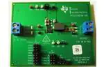
TPS53318 Step-Down Converter Evaluation Module User's
Guide
ABSTRACT
The TPS53319EVM-136 is designed to use a regulated 12-V bus to produce a regulated 1.5-V output at up to
14 A of load current. The TPS53319EVM-136 is designed to demonstrate the TPS53319 in a typical low voltage
application while providing a number of test points to evaluate the performance of the TPS53319.
Table of Contents
1 Introduction.............................................................................................................................................................................3
1.1 Typical Applications............................................................................................................................................................3
1.2 Features............................................................................................................................................................................. 3
2 Electrical Performance Specifications................................................................................................................................. 3
3 Schematic................................................................................................................................................................................4
4 Test Setup................................................................................................................................................................................5
4.1 Test Equipment.................................................................................................................................................................. 5
4.2 Recommended Test Setup.................................................................................................................................................6
5 Configurations........................................................................................................................................................................ 7
5.1 Switching Frequency Selection.......................................................................................................................................... 7
5.2 Soft Start Selection............................................................................................................................................................ 7
5.3 Mode Selection.................................................................................................................................................................. 7
5.4 Enable Selection................................................................................................................................................................ 7
6 Test Procedure........................................................................................................................................................................ 8
6.1 Line/Load Regulation and Efficiency Measurement Procedure......................................................................................... 8
6.2 Control Loop Gain and Phase Measurement Procedure................................................................................................... 8
6.3 List of Test Points............................................................................................................................................................... 8
6.4 Equipment Shutdown......................................................................................................................................................... 8
7 Performance Data and Typical Characteristic Curves........................................................................................................ 9
7.1 Efficiency............................................................................................................................................................................9
7.2 Load Regulation................................................................................................................................................................. 9
7.3 Line Regulation................................................................................................................................................................ 10
7.4 Enable Turn-On/ Turn-Off.................................................................................................................................................10
7.5 Output Ripple....................................................................................................................................................................11
7.6 Switching Node.................................................................................................................................................................11
7.7 Output Transient with Auto-skip Mode............................................................................................................................. 12
7.8 Output Transient with FCCM mode..................................................................................................................................12
7.9 Output 0.75-V Pre-bias Turn-On...................................................................................................................................... 13
7.10 Output Overcurrent and Short Circuit Protection........................................................................................................... 13
7.11 Bode plot........................................................................................................................................................................ 14
7.12 Thermal Image............................................................................................................................................................... 14
8 EVM Assembly Drawing and PCB Layout.......................................................................................................................... 15
9 Bill of Materials..................................................................................................................................................................... 23
10 Revision History................................................................................................................................................................. 23
List of Figures
Figure 3-1. TPS53319EVM-136 Schematic.................................................................................................................................4
Figure 4-1. Tip and Barrel Measurement for VOUT Ripple............................................................................................................5
Figure 4-2. TPS53319EVM-136 Recommended Test Setup....................................................................................................... 6
Figure 7-1. Efficiency................................................................................................................................................................... 9
Figure 7-2. Load Regulation........................................................................................................................................................ 9
Figure 7-3. Line Regulation....................................................................................................................................................... 10
SLVU728A – MAY 2012 – REVISED DECEMBER 2021
Submit Document Feedback
TPS53318 Step-Down Converter Evaluation Module User's Guide
Copyright © 2021 Texas Instruments Incorporated
1
�Table of Contents
www.ti.com
Figure 7-4. Enable Turn-On....................................................................................................................................................... 10
Figure 7-5. Enable Turn-Off....................................................................................................................................................... 10
Figure 7-6. Output Ripple...........................................................................................................................................................11
Figure 7-7. Switching Node........................................................................................................................................................11
Figure 7-8. Output Transient from DCM to CCM....................................................................................................................... 12
Figure 7-9. Output Transient from CCM to DCM....................................................................................................................... 12
Figure 7-10. Output Transient with FCCM mode....................................................................................................................... 12
Figure 7-11. Output 0.75-V Pre-bias Turn-On............................................................................................................................13
Figure 7-12. Output Overcurrent Protection.............................................................................................................................. 13
Figure 7-13. Output Overvoltage Protection.............................................................................................................................. 13
Figure 7-14. Bode plot at 12Vin, 1.5V/14A................................................................................................................................ 14
Figure 7-15. Top Board at 12 VIN, 1.5 V/14 A, 25°C Ambient Without Airflow........................................................................... 14
Figure 8-1. TPS53319EVM-136 Top Layer Assembly Drawing.................................................................................................15
Figure 8-2. TPS53319EVM-136 Bottom Assembly Drawing..................................................................................................... 16
Figure 8-3. TPS53319EVM-136 Top Copper.............................................................................................................................17
Figure 8-4. TPS53319EVM-136 Layer 2 Copper.......................................................................................................................18
Figure 8-5. TPS53319EVM-136 Layer 3 Copper.......................................................................................................................19
Figure 8-6. TPS53319EVM-136 Layer 4 Copper.......................................................................................................................20
Figure 8-7. TPS53319EVM-136 Layer 5 Copper.......................................................................................................................21
Figure 8-8. TPS53319EVM-136 Bottom Layer Copper............................................................................................................. 22
List of Tables
Table 2-1. TPS53319EVM-136 Electrical Performance Specifications........................................................................................3
Table 5-1. Switching Frequency Selection...................................................................................................................................7
Table 5-2. Soft Start Time Selection............................................................................................................................................ 7
Table 5-3. MODE Selection......................................................................................................................................................... 7
Table 5-4. Enable Selection......................................................................................................................................................... 7
Table 6-1. The Functions of Each Test Points............................................................................................................................. 8
Table 9-1. Components List....................................................................................................................................................... 23
2
TPS53318 Step-Down Converter Evaluation Module User's Guide
Copyright © 2021 Texas Instruments Incorporated
SLVU728A – MAY 2012 – REVISED DECEMBER 2021
Submit Document Feedback
�www.ti.com
Introduction
1 Introduction
The TPS53319EVM-136 evaluation module (EVM) uses the TPS53319. The TPS53319 is a D-CAP mode, 14-A
synchronous buck converter with integrated MOSFETs. The device provides a fixed 1.5-V output at up to 14 A
from a 12-V input bus.
1.1 Typical Applications
•
•
•
Server/storage
Workstations and desktops
Telecommunication infrastructure
1.2 Features
The TPS53319EVM-136 features:
•
•
•
•
•
•
•
14-A DC steady state output current
Support pre-bias output voltage start-up
J3 for selectable switching frequency setting
J4 for selectable soft-start time
J5 for auto-skip and forced CCM selection
J6 for enable function
Convenient test points for probing critical waveforms
2 Electrical Performance Specifications
Table 2-1. TPS53319EVM-136 Electrical Performance Specifications
PARAMETER(1)
TEST CONDITIONS
MIN
TYP
MAX
8
12
20
UNITS
INPUT CHARACTERISTICS
Voltage range
VIN
Maximum input current
VIN = 8 V, IO = 14 A
No load input current
VIN = 20 V, IO = 0 A with auto skip mode
2.874
V
A
0.7
mA
1.5
V
OUTPUT CHARACTERISTICS
Output voltage VOUT
Output voltage regulation
Line regulation (VIN = 8 V–20 V)
0.1%
Load regulation (VIN = 12 V, IO = 0 A–14 A), auto-skip
Output voltage ripple
1%
VIN = 12 V, IO = 14 A
15
Output load current
0
Output over current
mVpp
14
A
16
A
500
kHz
SYSTEMS CHARACTERISTICS
Switching frequency
Peak efficiency
VIN = 12 V, 1.5 V/8 A
91.68%
Full load efficiency
VIN = 12 V, 1.5 V/14 A
90.04%
Operating temperature
(1)
25
°C
Note: Jumpers set to default locations. See Section 6.
SLVU728A – MAY 2012 – REVISED DECEMBER 2021
Submit Document Feedback
TPS53318 Step-Down Converter Evaluation Module User's Guide
Copyright © 2021 Texas Instruments Incorporated
3
�Schematic
www.ti.com
3 Schematic
Figure 3-1. TPS53319EVM-136 Schematic
4
TPS53318 Step-Down Converter Evaluation Module User's Guide
Copyright © 2021 Texas Instruments Incorporated
SLVU728A – MAY 2012 – REVISED DECEMBER 2021
Submit Document Feedback
�www.ti.com
Test Setup
4 Test Setup
4.1 Test Equipment
Voltage Source:
The input voltage source, VIN, should be a 0-V to 20-V variable DC source capable of supplying 10 ADC. Connect
VIN to J1 as shown in Figure 4-2.
Multimeters:
V1: VIN at TP1 (VIN) and TP10 (GND). V2: VOUT at TP2 (VOUT) and TP11 (GND). A1: VIN input current
Output Load:
The output load should be an electronic constant resistance mode load capable of 0 ADC to 16 ADC at 1.5 V.
Oscilloscope:
A digital or analog oscilloscope can be used to measure the output ripple. The oscilloscope should be set for the
following:
•
•
•
•
•
1-MΩ impedance
20-MHz bandwidth
AC coupling
2-μs/division horizontal resolution
20-mV/division vertical resolution
Test points TP2 and TP11 can be used to measure the output ripple voltage by placing the oscilloscope probe tip
through TP2 and holding the ground barrel on TP11 as shown in Figure 4-1. Using a leaded ground connection
can induce additional noise due to the large ground loop.
Metal Ground Barrel
Probe Tip
TP2
TP11
Figure 4-1. Tip and Barrel Measurement for VOUT Ripple
Recommended Wire Gauge:
1. VIN to J1 (12-V input):
The recommended wire size is AWG #16 per input connection, with the total length of wire less than four feet
(two feet input, two feet return).
2. J2 to LOAD:
The minimum recommended wire size is AWG #14, with the total length of wire less than four feet (two feet
output, two feet return).
SLVU728A – MAY 2012 – REVISED DECEMBER 2021
Submit Document Feedback
TPS53318 Step-Down Converter Evaluation Module User's Guide
Copyright © 2021 Texas Instruments Incorporated
5
�Test Setup
www.ti.com
4.2 Recommended Test Setup
+
DC +
Source
Vin
-
V1
V2
Load
-
A1
Figure 4-2. TPS53319EVM-136 Recommended Test Setup
Figure 4-2 is the recommended test setup to evaluate the TPS53319EVM-136. Working at an ESD workstation,
make sure that any wrist straps, bootstraps, or mats are connected referencing the user to earth ground before
power is applied to the EVM.
Input Connections:
1. Prior to connecting the DC input source VIN, it is advisable to limit the source current from VIN to 10-A
maximum. Make sure VIN is initially set to 0 V and connected as shown in Figure 4-2.
2. Connect a voltmeter V1 at TP1 (VIN) and TP10 (GND) to measure the input voltage.
3. Connect a current meter A1 to measure the input current.
Output Connections
1. Connect the load to J2 and set the load to constant resistance mode to sink 0 ADC before VIN is applied.
2. Connect a voltmeter V2 at TP2 (VOUT) and TP11 (GND) to measure the output voltage.
6
TPS53318 Step-Down Converter Evaluation Module User's Guide
Copyright © 2021 Texas Instruments Incorporated
SLVU728A – MAY 2012 – REVISED DECEMBER 2021
Submit Document Feedback
�www.ti.com
Configurations
5 Configurations
All jumper selections should be made prior to applying power to the EVM. The user can configure this EVM per
the following configurations.
5.1 Switching Frequency Selection
The switching frequency can be set by J3.
Default setting: 500 kHz
Table 5-1. Switching Frequency Selection
JUMPER SET TO
RESISTOR (RF) CONNECTIONS (Ω)
SWITCHING FREQUENCY (kHz)
Top (1–2 pin shorted)
0
250
2nd (3–4 pin shorted)
187 k
300
3rd
(5–6 pin shorted)
619 k
400
4th (7–8 pin shorted)
Open
500
5th (9–10 pin shorted)
866 k
600
6th
(11–12 pin shorted)
309 k
750
7th (13–14 pin shorted)
124 k
850
Bottom (15–16 pin shorted)
0
970
5.2 Soft Start Selection
The soft start time can be set by J4.
Default setting: 1.4ms
Table 5-2. Soft Start Time Selection
Jumper set to
RMODE Connections(Ω)
Soft Start Time(ms)
Top(1-2 pin shorted)
39.2k
0.7
2nd
100k
1.4
3rd(5-6 pin shorted)
(3-4 pin shorted)
200k
2.8
Bottom(7-8 pin shorted)
475k
5.6
5.3 Mode Selection
The MODE can be set by J5.
Default setting: Auto Skip
Table 5-3. MODE Selection
Jumper set to
MODE Selection
Top(1-2 pin shorted)
Auto Skip
Bottom(3-4 pin shorted)
Forced CCM
5.4 Enable Selection
The controller can be enabled and disabled by J6.
Default setting: Jumper shorts on J6 to disable the controller
Table 5-4. Enable Selection
Jumper set to
Enable Selection
Jumper shorts on J6
Disable the controller
No Jumper shorts on J6
Enable the controller
SLVU728A – MAY 2012 – REVISED DECEMBER 2021
Submit Document Feedback
TPS53318 Step-Down Converter Evaluation Module User's Guide
Copyright © 2021 Texas Instruments Incorporated
7
�Test Procedure
www.ti.com
6 Test Procedure
6.1 Line/Load Regulation and Efficiency Measurement Procedure
1.
2.
3.
4.
5.
6.
7.
8.
9.
10.
11.
12.
Set up EVM as described in Section 4 and Figure 4-2.
Ensure Load is set to constant resistance mode and to sink 0Adc
Ensure all jumpers configuration settings per section 5.
Ensure the jumper provided in the EVM shorts on J6 before Vin is applied.
Increase Vin from 0V to 12V. Using V1 to measure input voltage.
Remove the jumper on J6 to enable the controller.
Use V2 to measure Vout voltage.
Vary Load from 0-14Adc, Vout should be remain in load regulation.
Vary Vin from 8V to 20V, Vout should remain in line regulation.
Put the jumper on J6 to disable the controller.
Decrease Load to 0A
Decrease Vin to 0V.
6.2 Control Loop Gain and Phase Measurement Procedure
TPS53319EVM-136 contains a 10Ω series resistor in the feedback loop for loop response analysis.
1. Set up EVM as described in Section 4 and Figure 4-2.
2. Connect isolation transformer to test points marked TP6 and TP7.
3. Connect input signal amplitude measurement probe (channel A) to TP6. Connect output signal amplitude
measurement probe (channel B) to TP7.
4. Connect ground lead of channel A and channel B to TP9.
5. Inject around 20mV or less signal through the isolation transformer.
6. Sweep the frequency from 100Hz to 1MHz with 10Hz or lower post filter. The control loop gain and phase
margin can be measured.
7. Disconnect isolation transformer from bode plot test points before making other measurements (Signal
injection into feedback may interfere with accuracy of other measurements).
6.3 List of Test Points
Table 6-1. The Functions of Each Test Points
Test Points
Name
Description
TP1
VIN
Controller input
TP2
Vout
Output Voltage
TP3
VREG
5V LDO output
TP4
PGOOD
Power Good
TP5
EN
Enable
TP6
CHA
Input A for loop injection
TP7
CHB
Input B for loop injection
TP8
LL
Switching node
TP9
GND
Ground
TP10
GND
Ground
TP11
GND
Ground
TP12
GND
Ground
6.4 Equipment Shutdown
1. Shut down the load.
2. Shut down VIN.
8
TPS53318 Step-Down Converter Evaluation Module User's Guide
Copyright © 2021 Texas Instruments Incorporated
SLVU728A – MAY 2012 – REVISED DECEMBER 2021
Submit Document Feedback
�www.ti.com
Performance Data and Typical Characteristic Curves
7 Performance Data and Typical Characteristic Curves
Figure 7-1 through Figure 7-15 present typical performance curves for TPS53319EVM-136.
7.1 Efficiency
Figure 7-1. Efficiency
7.2 Load Regulation
Figure 7-2. Load Regulation
SLVU728A – MAY 2012 – REVISED DECEMBER 2021
Submit Document Feedback
TPS53318 Step-Down Converter Evaluation Module User's Guide
Copyright © 2021 Texas Instruments Incorporated
9
�Performance Data and Typical Characteristic Curves
www.ti.com
7.3 Line Regulation
Figure 7-3. Line Regulation
7.4 Enable Turn-On/ Turn-Off
Figure 7-4. Enable Turn-On
10
Figure 7-5. Enable Turn-Off
TPS53318 Step-Down Converter Evaluation Module User's Guide
Copyright © 2021 Texas Instruments Incorporated
SLVU728A – MAY 2012 – REVISED DECEMBER 2021
Submit Document Feedback
�www.ti.com
Performance Data and Typical Characteristic Curves
7.5 Output Ripple
Figure 7-6. Output Ripple
7.6 Switching Node
Figure 7-7. Switching Node
SLVU728A – MAY 2012 – REVISED DECEMBER 2021
Submit Document Feedback
TPS53318 Step-Down Converter Evaluation Module User's Guide
Copyright © 2021 Texas Instruments Incorporated
11
�Performance Data and Typical Characteristic Curves
www.ti.com
7.7 Output Transient with Auto-skip Mode
Figure 7-8. Output Transient from DCM to CCM
Figure 7-9. Output Transient from CCM to DCM
7.8 Output Transient with FCCM mode
Figure 7-10. Output Transient with FCCM mode
12
TPS53318 Step-Down Converter Evaluation Module User's Guide
Copyright © 2021 Texas Instruments Incorporated
SLVU728A – MAY 2012 – REVISED DECEMBER 2021
Submit Document Feedback
�www.ti.com
Performance Data and Typical Characteristic Curves
7.9 Output 0.75-V Pre-bias Turn-On
Figure 7-11. Output 0.75-V Pre-bias Turn-On
7.10 Output Overcurrent and Short Circuit Protection
Figure 7-12. Output Overcurrent Protection
SLVU728A – MAY 2012 – REVISED DECEMBER 2021
Submit Document Feedback
Figure 7-13. Output Overvoltage Protection
TPS53318 Step-Down Converter Evaluation Module User's Guide
Copyright © 2021 Texas Instruments Incorporated
13
�Performance Data and Typical Characteristic Curves
www.ti.com
7.11 Bode plot
Figure 7-14. Bode plot at 12Vin, 1.5V/14A
7.12 Thermal Image
Figure 7-15. Top Board at 12 VIN, 1.5 V/14 A, 25°C Ambient Without Airflow
14
TPS53318 Step-Down Converter Evaluation Module User's Guide
Copyright © 2021 Texas Instruments Incorporated
SLVU728A – MAY 2012 – REVISED DECEMBER 2021
Submit Document Feedback
�www.ti.com
EVM Assembly Drawing and PCB Layout
8 EVM Assembly Drawing and PCB Layout
Figure 8-1 through Figure 8-8 show the design of the TPS53319EVM-136 printed circuit board. The EVM has
been designed using a 6-layer, 2-oz copper circuit board.
Figure 8-1. TPS53319EVM-136 Top Layer Assembly Drawing
SLVU728A – MAY 2012 – REVISED DECEMBER 2021
Submit Document Feedback
TPS53318 Step-Down Converter Evaluation Module User's Guide
Copyright © 2021 Texas Instruments Incorporated
15
�EVM Assembly Drawing and PCB Layout
www.ti.com
Figure 8-2. TPS53319EVM-136 Bottom Assembly Drawing
16
TPS53318 Step-Down Converter Evaluation Module User's Guide
Copyright © 2021 Texas Instruments Incorporated
SLVU728A – MAY 2012 – REVISED DECEMBER 2021
Submit Document Feedback
�www.ti.com
EVM Assembly Drawing and PCB Layout
Figure 8-3. TPS53319EVM-136 Top Copper
SLVU728A – MAY 2012 – REVISED DECEMBER 2021
Submit Document Feedback
TPS53318 Step-Down Converter Evaluation Module User's Guide
Copyright © 2021 Texas Instruments Incorporated
17
�EVM Assembly Drawing and PCB Layout
www.ti.com
Figure 8-4. TPS53319EVM-136 Layer 2 Copper
18
TPS53318 Step-Down Converter Evaluation Module User's Guide
Copyright © 2021 Texas Instruments Incorporated
SLVU728A – MAY 2012 – REVISED DECEMBER 2021
Submit Document Feedback
�www.ti.com
EVM Assembly Drawing and PCB Layout
Figure 8-5. TPS53319EVM-136 Layer 3 Copper
SLVU728A – MAY 2012 – REVISED DECEMBER 2021
Submit Document Feedback
TPS53318 Step-Down Converter Evaluation Module User's Guide
Copyright © 2021 Texas Instruments Incorporated
19
�EVM Assembly Drawing and PCB Layout
www.ti.com
Figure 8-6. TPS53319EVM-136 Layer 4 Copper
20
TPS53318 Step-Down Converter Evaluation Module User's Guide
Copyright © 2021 Texas Instruments Incorporated
SLVU728A – MAY 2012 – REVISED DECEMBER 2021
Submit Document Feedback
�www.ti.com
EVM Assembly Drawing and PCB Layout
Figure 8-7. TPS53319EVM-136 Layer 5 Copper
SLVU728A – MAY 2012 – REVISED DECEMBER 2021
Submit Document Feedback
TPS53318 Step-Down Converter Evaluation Module User's Guide
Copyright © 2021 Texas Instruments Incorporated
21
�EVM Assembly Drawing and PCB Layout
www.ti.com
Figure 8-8. TPS53319EVM-136 Bottom Layer Copper
22
TPS53318 Step-Down Converter Evaluation Module User's Guide
Copyright © 2021 Texas Instruments Incorporated
SLVU728A – MAY 2012 – REVISED DECEMBER 2021
Submit Document Feedback
�www.ti.com
Bill of Materials
9 Bill of Materials
Table 9-1 list the EVM components according to the schematic shown in Figure 3-1.
Table 9-1. Components List
QTY.
RefDes
Description
MFR
Part Number
2
C1, C2
Capacitor, Ceramic, 22 μF, 25 V, X5R, 20%, 1210
STD
STD
3
C7, C8, C9
Capacitor, Ceramic, 100 μF, 6.3 V, X5R, 20%, 1210
STD
STD
1
C13
Capacitor, Ceramic, 4.7 μF, 25 V, X5R, 20%, 0805
STD
STD
1
C14
Capacitor, Ceramic, 1 μF, 50 V, X7R, 10%, 0603
STD
STD
2
C18, C19
Capacitor, Ceramic, 1000 pF, 50 V, X7R, 10%, 0603
STD
STD
3
C5, C15, C17
Capacitor, Ceramic, 0.1 μF, 50 V, X7R, 10%, 0603
STD
STD
1
C20
Capacitor, Ceramic, 100 pF, 50 V, X7R, 10%, 0603
STD
STD
1
L1
Inductor, SMT, 500 nH±15%, 17 A, DCR: 0.29 mΩ±10%, 7 mm × 11 mm
Delta
HCB1175-501TI
1
R1
Resistor, Chip, 0, 1/16W, 1%, 0603
STD
STD
1
R7
Resistor, Chip, 3.01, 1/16W, 1%, 0603
STD
STD
2
R10, R23
Resistor, Chip, 14.7 k, 1/16W, 1%, 0603
STD
STD
1
R11
Resistor, Chip, 10, 1/16W, 1%, 0603
STD
STD
1
R13
Resistor, Chip, 187 k, 1/16W, 1%, 0603
STD
STD
1
R14
Resistor, Chip, 619 k, 1/16W, 1%, 0603
STD
STD
1
R16
Resistor, Chip, 866 k, 1/16W, 1%, 0603
STD
STD
1
R17
Resistor, Chip, 309 k, 1/16W, 1%, 0603
STD
STD
1
R18
Resistor, Chip, 124 k, 1/16W, 1%, 0603
STD
STD
1
R19
Resistor, Chip, 39.2 k, 1/16W, 1%, 0603
STD
STD
1
R2
Resistor, Chip, 169 k, 1/16W, 1%, 0603
STD
STD
1
R22
Resistor, Chip, 475 k, 1/16W, 1%, 0603
STD
STD
2
R3, R21
Resistor, Chip, 200 k, 1/16W, 5%, 0603
STD
STD
1
R4
Resistor, Chip, 86.6 k, 1/16W, 1%, 0603
STD
STD
1
R5
Resistor, Chip, 1.00 k, 1/16W, 1%, 0603
STD
STD
2
R6, R20
Resistor, Chip, 100 k, 1/16W, 1%, 0603
STD
STD
1
R9
Resistor, Chip, 3.01 k, 1/16W, 1%, 0603
STD
STD
2
R12, R24
Resistor, Chip, 10.0 k, 1/16W, 1%, 0603
STD
STD
1
U1
IC, 14-A synchronous buck converter with integrated MOSFETs, DQP-22
TI
TPS53319DQP
10 Revision History
NOTE: Page numbers for previous revisions may differ from page numbers in the current version.
Changes from Revision * (May 2012) to Revision A (December 2021)
Page
• Updated the numbering format for tables, figures, and cross-references throughout the document. ................3
• Updated the user's guide title............................................................................................................................. 3
SLVU728A – MAY 2012 – REVISED DECEMBER 2021
Submit Document Feedback
TPS53318 Step-Down Converter Evaluation Module User's Guide
Copyright © 2021 Texas Instruments Incorporated
23
�IMPORTANT NOTICE AND DISCLAIMER
TI PROVIDES TECHNICAL AND RELIABILITY DATA (INCLUDING DATA SHEETS), DESIGN RESOURCES (INCLUDING REFERENCE
DESIGNS), APPLICATION OR OTHER DESIGN ADVICE, WEB TOOLS, SAFETY INFORMATION, AND OTHER RESOURCES “AS IS”
AND WITH ALL FAULTS, AND DISCLAIMS ALL WARRANTIES, EXPRESS AND IMPLIED, INCLUDING WITHOUT LIMITATION ANY
IMPLIED WARRANTIES OF MERCHANTABILITY, FITNESS FOR A PARTICULAR PURPOSE OR NON-INFRINGEMENT OF THIRD
PARTY INTELLECTUAL PROPERTY RIGHTS.
These resources are intended for skilled developers designing with TI products. You are solely responsible for (1) selecting the appropriate
TI products for your application, (2) designing, validating and testing your application, and (3) ensuring your application meets applicable
standards, and any other safety, security, regulatory or other requirements.
These resources are subject to change without notice. TI grants you permission to use these resources only for development of an
application that uses the TI products described in the resource. Other reproduction and display of these resources is prohibited. No license
is granted to any other TI intellectual property right or to any third party intellectual property right. TI disclaims responsibility for, and you
will fully indemnify TI and its representatives against, any claims, damages, costs, losses, and liabilities arising out of your use of these
resources.
TI’s products are provided subject to TI’s Terms of Sale or other applicable terms available either on ti.com or provided in conjunction with
such TI products. TI’s provision of these resources does not expand or otherwise alter TI’s applicable warranties or warranty disclaimers for
TI products.
TI objects to and rejects any additional or different terms you may have proposed. IMPORTANT NOTICE
Mailing Address: Texas Instruments, Post Office Box 655303, Dallas, Texas 75265
Copyright © 2022, Texas Instruments Incorporated
�


 工商网监
湘ICP备2023018690号
工商网监
湘ICP备2023018690号
