Product
Folder
Order
Now
Support &
Community
Tools &
Software
Technical
Documents
TPS53667
SLUSC40B – JULY 2016 – REVISED FEBRUARY 2017
TPS53667 6-Phase, D-CAP+, Step-Down, Buck Controller with NVM
and PMBus™ Interface for ASIC Power and High-Current Point-of-Load
Check for Samples: TPS53667
1 Features
3 Description
•
The TPS53667 is a high-current, multi-phase, stepdown controller. The device offers built-in non volatile
memory (NVM) and PMBus interface. It is compatible
with the NexFET power stages (CSD9549x). The
TPS53667 provides 8-bit BOOT voltage selection
covering output voltage from 0.5 V to 2.5 V, with
steps as small as 5 mV, which is ideal for high
current application with accurate output voltage
setting. Advanced control features such as D-CAP+
architecture with undershoot reduction (USR) and
overshoot reduction (OSR) provide fast transient
response, lowest output capacitance, and high
efficiency. The TPS53667 also provides novel phase
interleaving strategy and dynamic phase shedding for
efficiency improvement at light loads. In addition, the
TPS53667 supports the PMBus communication
interface with systems for telemetry of voltage,
current, power, temperature, and fault conditions.
Some of the configurations can be programmed by
pinstrap or PMBus and stored in non-volatile memory
to minimize the external component count.
1
•
•
•
•
•
•
•
•
•
•
•
•
•
•
•
•
•
•
•
•
8-bit Selectable BOOT Voltage via Pinstrap or
NVM: 0.5 V to 2.5 V (down to 5-mV Step)
1-, 2-, 3-, 4-, 5-, or 6- Phase Operation
PMBus™ System Interface for Telemetry of
Voltage, Current, Power, Temperature, and Fault
Conditions
1.8-V and 3.3-V PMBus Bias Compatible
Fault Reporting: Output Voltage, Output Current,
and Temperature
Configurable with Non-Volatile Memory (NVM) or
Resistor Pinstrap
16 Levels of Programmable Per-Phase OCL with
Pinstrap or NVM
Fast Transient with DCAP+™Control
Optimized Efficiency at Light and Heavy Loads
Support Pre-Bias Startup
Phase Current Imbalance Detection and
Reporting
8 Independent Levels of Overshoot Reduction
(OSR) and Undershoot Reduction (USR)
Driverless Configuration for Efficient HighFrequency Switching
Compatible with CSD9549x NexFET™ Power
Stages
Accurate, Adjustable Voltage Positioning
300-kHz to 1-MHz Frequency Selections with
Closed-loop Frequency Control
Patented AutoBalance™ Phase Balancing
Uses TI’s Fusion Digital Power Designer GUI
Dynamic Phase Shedding with Programmable
Current Threshold
Conversion Voltage Range: 4.5 V to 17 V
Small, 6 mm × 6 mm, 40-Pin, QFN, PowerPAD™
Package
The TPS53667 is offered in a space saving, thermally
enhanced 40-pin QFN package and is rated to
operate from –40°C to 125°C.
Device Information(1)
PART NUMBER
PACKAGE
BODY SIZE (NOM)
TPS53667
QFN (40)
6.00 mm × 6.00 mm
(1) For all available packages, see the orderable addendum at
the end of the datasheet.
Simplified Schematic
TPS53667
PWM1
CSP1
PMBus
PWM2
CSP2
Power
Stage
Power
Stage
2 Applications
•
•
•
•
Application-Specific Integrated Circuit (ASIC)
Power in Communications Equipment
High Density Power Solutions
Server Power
Smart Power Systems
PWM6
CSP6
Power
Stage
Copyright © 2016, Texas Instruments Incorporated
1
An IMPORTANT NOTICE at the end of this data sheet addresses availability, warranty, changes, use in safety-critical applications,
intellectual property matters and other important disclaimers. PRODUCTION DATA.
�TPS53667
SLUSC40B – JULY 2016 – REVISED FEBRUARY 2017
www.ti.com
4 Revision History
Changes from Revision A (September 2016) to Revision B
Page
•
Updated V3R3 LDO section ................................................................................................................................................. 20
•
Added temperature default value VR_HOT and VR_FAULT Indication section ................................................................. 33
•
Corrected factory default value of VOUT_OV_FAULT_RESPONSE command in Table 7 ................................................. 40
•
Corrected factory default value of VIN_OV_FAULT_LIMIT command in Table 7................................................................ 40
•
Corrected factory default value of MFR_ID command in Table 7 ........................................................................................ 41
•
Corrected factory default value of MFR_SPECIFIC_44 command in Table 7 ..................................................................... 42
Changes from Original (July 2016) to Revision A
Page
•
Changed data sheet status from Product Preview to Production Data .................................................................................. 1
•
Added Receiving Notification of Documentation Updates section ..................................................................................... 117
•
Added Community Resources section ............................................................................................................................... 117
2
Submit Documentation Feedback
Copyright © 2016–2017, Texas Instruments Incorporated
Product Folder Links: TPS53667
�TPS53667
www.ti.com
SLUSC40B – JULY 2016 – REVISED FEBRUARY 2017
5 Pin Configuration and Functions
TSEN
SKIP-NVM
PWM1
PWM2
PWM3
PWM4
PWM5
PWM6
F-IMAX
VBOOT
RTA Package
40-Pin QFN
Top View
40
39
38
37
36
35
34
33
32
31
OCL-R 1
30
O-USR
IMON 2
29
SLEW-MODE
CSP1 3
28
ADDR-TRISE
CSP2
4
27
VR_FAULT
CSP3
5
26
PMB_DIO
CSP4
6
25
PMB_ALERT
CSP5
7
24
PMB_CLK
CSP6
8
23
ENABLE
VSP
9
22
GND
21
RESET
TPS53667
Thermal Pad
V3R3
17
18
19
20
GND
VREF
16
VR_HOT
ISUM
15
VR_RDY
14
GND
13
VIN
12
V5
11
COMP
VSN 10
Pin Functions
PIN
NAME
NO.
I/O (1)
DESCRIPTION
ADDR-TRISE
28
I
Voltage divider to VREF pin. A resistor (RADDR-TRISE) connected between this pin and GND sets the
3-bits. Bit 2 and bit 1 set the rise slew rate. Bit 0 Selects the LSB of BOOT voltage. The voltage
(VADDR-TRISE) sets 4 bits PMBus address. The device latches these settings when V3R3 powers up.
COMP
11
O
Output of the gM error amplifier. Resistors and capacitors connected between this pin and the VREF
pin set the compensation.
CSP1
3
CSP2
4
CSP3
5
CSP4
6
I
Positive current sense inputs. Connect to the IOUT pin of TI smart power stages (ex: CSD9549x). Tie
CSP6, CSP5, CSP4, CSP3, or CSP2 to the V3R3 pin according to Table 3 to disable the
corresponding phase.
CSP5
7
CSP6
8
ENABLE
23
I
VR enable. 1-V I/O level; 100-ns debounce.
F-IMAX
32
I
Voltage divider to VREF pin. A resistor (RF-IMAX) connected between this pin and GND sets the
operating frequency of the controller. The voltage level (VF-IMAX) sets the maximum operating current
of the converter. The IMAX value is an 8-bit A/D where VF-IMAX = VVREF × IMAX / 255. Both are latched
at V3R3 power-up.
GND
17
G
Ground pin.
G
Connect these pins to GND. Note this is not IC ground pin.
GND
(1)
20
22
I = Input, O = Output, P = Power, I/O = Bi-directional, GND = ground
Submit Documentation Feedback
Copyright © 2016–2017, Texas Instruments Incorporated
Product Folder Links: TPS53667
3
�TPS53667
SLUSC40B – JULY 2016 – REVISED FEBRUARY 2017
www.ti.com
Pin Functions (continued)
PIN
NAME
NO.
IMON
2
I/O (1)
O
DESCRIPTION
I ´ 5mW ´ RIMON
VIMON = O
35kW
Analog current monitor output.
A resistor (RISUM) connected between this pin and VREF pin determines the droop.
ISUM
12
O
VISUM =
IO ´ 5mW ´ gM(isum ) ´ RISUM
n
+ VREF
(where n is the number of phases)
OCL-R
1
I
A resistor (ROCL-R) connected between this pin and GND and the voltage level (VOCL-R) select 1 of 16
OCL levels (per phase current-limit). VOCL-R also sets one of four RAMP levels. The device latches
these settings when V3R3 powers up.
O-USR
30
I
Voltage divider to VREF pin. A resistor (RO-USR) connected between this pin and GND selects one of
seven OSR thresholds or OFF. The voltage level (VO-USR) sets one of seven USR levels or OFF. The
device latches these settings when V3R3 powers up.
PMB_ALERT
25
O
I2C PMBus interrupt line. Open drain. 3.3-V and 1.8-V logic level.
PMB_CLK
24
I
I2C PMBus clock. 3.3-V and 1.8-V logic level.
PMB_DIO
26
I/O
I2C PMBus digital I/O line. 3.3-V and 1.8-V logic level.
PWM1
38
PWM2
37
PWM3
36
PWM4
35
O
PWM signals for each phase
PWM5
34
PWM6
33
RESET
21
I
Reset pin. If this pin is low for more than 1000 ns, the controller pulls the output voltage to the VBOOT
level.
SKIP-NVM
39
O
A resistor (R SKIP-NVM) connected between this pin and GND sets either pinstrap or NVM configuration
mode. This pin can also connect to the FCCM pin of TI smart power stages (ex: CSD9549x) for SKIP
or FCCM operation.
SLEW-MODE
29
I
Voltage divider to VREF pin. A resistor (RSLEW-MODE) connected between this pin and GND sets 8
slew rates. The voltage level (VSLEW-MODE) sets 4-bit operation modes. Bit 7 for DAC mode (1 for
VR12.0; 0 for VR12.5). Bit 6 for the 4-phase interleaving mode (1 for 1/3 and 2/4 two phase
interleaving; 0 for 4 phase interleaving individually). Bit 4 for enabling dynamic phase add or drop (1
for enable; 0 for disable). Bit 3 sets zero load-line (1 for zero load-line; 0 for non-zero load-line) The
device latches these settings when V3R3 powers up.
TSEN
40
I
Connect to the TAO/FAULT pin of TI smart power stages (ex: CSD9549x) to sense the highest
temperature of the power stages and to sense the fault signal from the power stages.
V3R3
14
O
3.3-V LDO output. Bypass this pin to GND with a ceramic capacitor with a value of 1-µF or larger.
V5
15
P
5-V power input. Bypass this pin to GND with a ceramic capacitor with a value of 1-µF or larger. This
pin is used to power all internal analog circuits.
VBOOT
31
I
Voltage divider to VREF pin. A resistor (RVBOOT) connected between this pin and GND sets 3 bits
(B[3:1]). The voltage level (VVBOOT) sets 4 bits (B[7:4]). The total 7 bits set 7 of 8 bits of VID of boot
voltage (B[7:1]). The device latches these settings when V3R3 powers up.
VIN
16
P
Input voltage supply. This pin is also used for input voltage sensing for on-time control and input
undervoltage lockout (UVLO).
VR_RDY
18
O
Power good open-drain output for the controller. This pin is typically pulled up to V3R3 pin through a
resistor with a value of 3-kΩ or larger.
VR_FAULT
27
O
VR fault indicator (open-drain). The failures include shorts of the high-side FETs, over temperature,
output overvoltage, and overcurrent conditions of the input. The fault signal should be used on the
platform to remove the power source either by firing a shunting SCR to blow a fuse or by turning off
the AC power supply. When the failure occurs, the VR_FAULT pin is LOW. This pin is typically pulled
up to V3R3 pin through a resistor with a value of 3-kΩ or larger. Leave this pin floating if not used.
VR_HOT
19
O
Thermal flag open drain output. Active low. This pin is typically pulled up to V3R3 pin through a
resistor with a value of 3-kΩ or larger. Leave this pin floating if not used.
4
Submit Documentation Feedback
Copyright © 2016–2017, Texas Instruments Incorporated
Product Folder Links: TPS53667
�TPS53667
www.ti.com
SLUSC40B – JULY 2016 – REVISED FEBRUARY 2017
Pin Functions (continued)
PIN
I/O (1)
DESCRIPTION
13
O
1.7-V, 500-µA, LDO reference voltage. Bypass this pin to GND with a ceramic capacitor with a value
of 0.33 µF. Connect the VREF pin to the REFIN pin of TI smart power stages (ex: CSD9549x) as the
current-sense reference voltage.
VSN
10
I
Negative input of the remote voltage sense amplifier. Connect this pin directly to the GND of the load.
VSP
9
I
Positive input of the remote voltage sense amplifier. Connect this pin directly to the load.
NAME
NO.
VREF
Thermal Pad
GND
Thermal pad. Connect the thermal pad to the ground plane with multiple vias.
6 Specifications
6.1 Absolute Maximum Ratings
over operating free-air temperature range (unless otherwise noted)
Input Voltage
Output Voltage
(1) (2)
MIN
MAX
VIN
–0.3
19
V5
–0.3
6
ADDR-TRISE, CSP1, CSP2, CSP3, CSP4, CSP5, CSP6, ENABLE, F-IMAX, OCLR, O-USR, PMB_CLK, PMB_DIO, RESET, SLEW-MODE, VBOOT, VSP
–0.3
3.6
TSEN
–0.3
6
GND, VSN
–0.3
0.3
VREF
–0.3
1.8
IMON, ISUM,PMB_ALERT, PWM1, PWM2, PWM3, PWM4, PWM5, PWM6, SKIPNVM, V3R3, VR_RDY, VR_FAULT, VR_HOT
–0.3
3.6
COMP
–0.3
6
–40
150
Operating Junction Temperature, TJ
(1)
(2)
UNIT
V
V
°C
Stresses beyond those listed under Absolute Maximum Ratings may cause permanent damage to the device. These are stress ratings
only, which do not imply functional operation of the device at these or any other conditions beyond those indicated under Recommended
Operating Conditions. Exposure to absolute-maximum-rated conditions for extended periods may affect device reliability.
All voltage values are with respect to the network ground terminal GND unless otherwise noted.
6.2 Handling Ratings
Tstg
V(ESD)
(1)
(2)
MIN
MAX
UNIT
–55
150
°C
Human body model (HBM), per ANSI/ESDA/JEDEC JS-001, all pins (1)
-2.5
2.5
Charged device model (CDM), per JEDEC specification JESD22-C101,
all pins (2)
-1.5
1.5
Storage temperature range
Electrostatic
discharge
kV
JEDEC document JEP155 states that 500-V HBM allows safe manufacturing with a standard ESD control process.
JEDEC document JEP157 states that 250-V CDM allows safe manufacturing with a standard ESD control process.
Submit Documentation Feedback
Copyright © 2016–2017, Texas Instruments Incorporated
Product Folder Links: TPS53667
5
�TPS53667
SLUSC40B – JULY 2016 – REVISED FEBRUARY 2017
www.ti.com
6.3 Recommended Operating Conditions
over operating free-air temperature range (unless otherwise noted)
VIN
TSEN
VI
Input voltage
MIN
NOM
4.5
12
MAX
17
-0.1
5.5
V5
4.5
ADDR-TRISE, F-IMAX, OCL-R, O-USR, SLEW-MODE,
VBOOT
0.1
VVREF
CSP1, CSP2, CSP3, CSP4, CSP5, CSP6, VSP
–0.1
2.5
ENABLE, PMB_CLK, PMB_DIO
–0.1
3.5
GND, VSN
–0.1
0.1
VREF
–0.1
1.72
5
5.5
V3R3
-0.1
IMON, ISUM, PMB_ALERT, PWM1, PWM2, PWM3, PWM4,
PWM5, PWM6, SKIP-NVM, VR_RDY, VR_FAULT, VR_HOT
–0.1
COMP
–0.1
5.5
–40
125
VO
Output voltage
TA
Operating free air temperature
UNIT
3.3
V
3.5
3.5
V
°C
6.4 Thermal Information
TPS53667
THERMAL METRIC
(1)
RTA (QFN)
UNIT
40 PINS
RθJA
Junction-to-ambient thermal resistance
30.6
RθJC(top)
Junction-to-case (top) thermal resistance
14.2
RθJB
Junction-to-board thermal resistance
6.9
ψJT
Junction-to-top characterization parameter
0.2
ψJB
Junction-to-board characterization parameter
6.8
RθJC(bot)
Junction-to-case (bottom) thermal resistance
1.8
(1)
6
°C/W
For more information about traditional and new thermal metrics, see the IC Package Thermal Metrics application report, SPRA953.
Submit Documentation Feedback
Copyright © 2016–2017, Texas Instruments Incorporated
Product Folder Links: TPS53667
�TPS53667
www.ti.com
SLUSC40B – JULY 2016 – REVISED FEBRUARY 2017
6.5 Electrical Characteristics
over recommended free-air temperature range, VVIN = 12 V, VV5 = 5 V, VVSN = GND, VVSP = VOUT (unless otherwise noted).
PARAMETER
TEST CONDITIONS
MIN
TYP
MAX
UNIT
SUPPLY: CURRENTS, UVLO, AND POWER-ON RESET
IVIN
VIN supply current, 6-phase active
VVDAC < VVSP < VVDAC + 100 mV, ENABLE = HI
IV5
V5 supply current
PMBus Idle, ENABLE = HI
IV5SBY
V5 standby current
ENABLE = LO
VV3R3
V3R3 output voltage
IV3R3 = 0 A
VV3R3(dropout)
V3R3 load regulation
IV3R3 = 5 mA
VV5UVLOH
V5 UVLO OK threshold
Ramp up
4.1
VV5UVLOL
V5 UVLO fault threshold
Ramp down
3.95
VHYS(V5)
V5 UVLO hysteresis
Hysteresis
VVINUVLO
VIN UVLO voltage
VHYS(VIN)
VIN UVLO hysteresis voltage
115
µA
6.1
7
mA
2
2.6
mA
3.3
3.4
V
100
mV
4.25
4.5
V
4.05
4.25
V
0.15
0.23
0.3
V
MFR_SPEC_16[1:0] = 00
4.2
4.5
4.7
MFR_SPEC_16[1:0] = 01
6.9
7.25
7.45
MFR_SPEC_16[1:0] = 10
7.6
7.9
8.2
MFR_SPEC_16[1:0] = 11
9.8
10.3
10.7
3.2
V
Hysteresis voltage
1.05
V
REFERENCES: DAC AND VREF
VR12.5: Change VID0 HI to LO to HI
10
VR12.0: Change VID0 HI to LO to HI
5
VVIDSTP
VID Step size
VDAC1
Closed Loop VSP tolerance
VR12.0: 0.61 V ≤ VVSP ≤ 0.995 V, IOUT = 0 A , 0 °C ≤ TA≤ 85 °C
VDAC2
Closed Loop VSP tolerance
VR12.0: 1 V ≤ VVSP ≤ 1.52 V, ICOUT = 0 A, 0 °C ≤ TA≤ 85 °C
VDAC3
Closed Loop VSP tolerance
VDAC4
mV
mV
–6
6.5
mV
–0.6
0.6
%
VR12.5: 1.50V ≤ VVSP ≤ 2.50 V, IOUT = 0 A, 0 °C ≤ TA≤ 85 °C
–1
1
%
Closed Loop VSP tolerance
VR12.0: 0.61 V ≤ VVSP ≤ 0.995 V, IOUT = 0 A, –40°C ≤ TA≤ 125
°C
–8
8
mV
VDAC5
Closed Loop VSP tolerance
VR12.0: 1.0 V ≤ VVSP ≤ 1.52 V, IOUT = 0 A, –40 °C ≤ TA≤ 125 °C
-0.8
0.8
%
VDAC6
Closed Loop VSP tolerance
VR12.5: 1.50 V ≤ VVSP ≤ 2.50V, IOUT = 0 A, –40°C ≤ TA≤ 125 °C
-1.1
1.0
%
VVREF
VREF output
4.5 ≤ VV5 ≤ 5.5 V, IVREF = 0 A
VVREFSRC
VREF output source
IVREF = 0 to 500 µA
VVREFSNK
VREF output sink
IVREF = –500 to 0 µA
1.685
1.70
–4
-1
1
1.717
V
mV
4
mV
CURRENT SENSE: AMPLIFIER AND PHASE BALANCING
GCSINT
Internal current sense gain
Gain from (CSPx – VREF ) to PWM comparator
1.0
V/V
µS
COMPENSATOR: VOLTAGE POSITIONING AND AMPLIFIER
gM(isum)
ISUM amplifier transconductance
VVSP = 1.7 V
500
gM(comp)
COMP amplifier transconductance
VVSP = 1.7 V
1000
µS
VCCLAMPN
COMP amplifier negative clamp voltage
(VVREF – VCOMP)
VRAMP + 20
mV
VCCLAMPP
COMP amplifier positive clamp voltage
(VCOMP – VVREF)
2.1
2.2
2.3
V
300
µA
VOLTAGE SENSE: VSP AND VSN
IVSP
VSP input bias current
Not in fault, disable or UVLO,
VVSP = VVDAC = 2.3 V, VVSN = 0 V
IVSN
VSN input bias current
Not in fault, disable or UVLO,
VVSP = VVDAC = 2.3 V, VVSN = 0 V
RSFTSTP
Transistor resistance
Connect to VSP
-30
-23
µA
10
kΩ
LOGIC ( RESET, VR_RDY, VR_FAULT, VR_HOT, AND ENABLE) INTERFACE PINS: I/O VOLTAGE AND CURRENT
RRPGDL
Open drain pull-down resistance
VR_RDY, pulldown resistance at 0.31 V
IVRTTLK
Open drain leakage current
VR_HOT, VR_RDY, hi-Z leakage, apply 3.3 V in off state
VRSTL
RESET logic low
RESET Pin
VRSTH
RESET logic high
RESET Pin
TRSTTDLY
RESET Delay Time
VENL
ENABLE logic low
VENH
ENABLE logic high
IENH
I/O 1.1- V leakage
–2
36
50
Ω
0.2
2
µA
0.8
V
1.2
V
1
µs
0.3
V
25
µA
0.8
V
0.8
Leakage current , VENABLE = 1.1 V
V
PMBUS INTERFACE PINS: I/O VOLTAGE AND CURRENT
VPMBL
PMBus pins logic low
VPMBH
PMBus pins logic high
IPMBL
Logic low input current
VPMBus=0 V
-10
10
µA
IPMBH
Logic high input current
VPMBus=1.8 V
-10
10
µA
1.2
V
Submit Documentation Feedback
Copyright © 2016–2017, Texas Instruments Incorporated
Product Folder Links: TPS53667
7
�TPS53667
SLUSC40B – JULY 2016 – REVISED FEBRUARY 2017
www.ti.com
Electrical Characteristics (continued)
over recommended free-air temperature range, VVIN = 12 V, VV5 = 5 V, VVSN = GND, VVSP = VOUT (unless otherwise noted).
PARAMETER
TEST CONDITIONS
MIN
TYP
MAX
UNIT
ADDR-TRISE PIN: PMBUS ADDRESS, SOFT START RISE TIME SETTING
SLRISE
BOOT
PADDR
8
Soft start rise slew rate in terms of VOUT
slew rate
BOOT voltage set (B0)
PMBus address bits set (11P40P2P1P0)
RADDR-TRISE ≤ 20 kΩ or RADDR-TRISE = 24 kΩ or
MFR_SPEC_12 = 00b
1
RADDR-TRISE = 30 kΩ or RADDR-TRISE = 39 kΩ or
MFR_SPEC_12 = 01b
1/2
RADDR-TRISE = 56 kΩ or RADDR-TRISE = 75 kΩ or
MFR_SPEC_12 = 10b
1/4
RADDR-TRISE = 100 kΩ or RADDR-TRISE = 150 kΩ or
MFR_SPEC_12 = 11b
1/8
RADDR-TRISE ≤ 20 kΩ or RADDR-TRISE = 30 kΩ or RADDR-TRISE = 56
kΩ or RADDR-TRISE = 100 kΩ, or MFR_SPEC_11 [0] = 0b
0
RADDR-TRISE = 24 kΩ or RADDR-TRISE = 39 kΩ or RADDR-TRISE = 75
kΩ or RADDR-TRISE = 150 kΩ, or MFR_SPEC_11 [0] = 1b
1
VADDR-TRISE ≤ 0.053 V with ±20 mV tolerance
1100000
VADDR-TRISE = 0.159 V with ±20 mV tolerance
1100001
VADDR-TRISE = 0.266 V with ±20 mV tolerance
1100010
VADDR-TRISE = 0.372 V with ±20 mV tolerance
1100011
VADDR-TRISE = 0.478 V with ±20 mV tolerance
1100100
VADDR-TRISE = 0.584 V with ±20 mV tolerance
1100101
VADDR-TRISE = 0.691 V with ±20 mV tolerance
1100110
VADDR-TRISE = 0.797 V with ±20 mV tolerance
1100111
VADDR-TRISE = 0.903 V with ±20 mV tolerance
1110000
VADDR-TRISE = 1.009 V with ±20 mV tolerance
1110001
VADDR-TRISE = 1.116 V with ±20 mV tolerance
1110010
VADDR-TRISE = 1.222 V with ±20 mV tolerance
1110011
VADDR-TRISE = 1.328 V with ±20 mV tolerance
1110100
VADDR-TRISE = 1.434 V with ±20 mV tolerance
1110101
VADDR-TRISE = 1.541 V with ±20 mV tolerance
1110110
VADDR-TRISE = 1.615 V with ±10 mV tolerance
1110111
Submit Documentation Feedback
Copyright © 2016–2017, Texas Instruments Incorporated
Product Folder Links: TPS53667
�TPS53667
www.ti.com
SLUSC40B – JULY 2016 – REVISED FEBRUARY 2017
Electrical Characteristics (continued)
over recommended free-air temperature range, VVIN = 12 V, VV5 = 5 V, VVSN = GND, VVSP = VOUT (unless otherwise noted).
PARAMETER
TEST CONDITIONS
MIN
TYP
MAX
ROCL-R = 20 kΩ and VOCL-R ≤ 0.85 V or
MFR_SPEC_00[3:0] = 0000b
21
24
27
ROCL-R = 24 kΩ and VOCL-R ≤ 0.85 V or
MFR_SPEC_00[3:0] = 0001b
25
27
30
ROCL-R = 30 kΩ and VOCL-R ≤ 0.85 V or
MFR_SPEC_00[3:0] = 0010b
28
30
33
ROCL-R = 39 kΩ and VOCL-R ≤ 0.85 V or
MFR_SPEC_00[3:0] = 0011b
31
33
36
ROCL-R = 56 kΩ and VOCL-R ≤ 0.85 V or
MFR_SPEC_00[3:0] = 0100b
34
36
39
ROCL-R = 75 kΩ and VOCL-R ≤ 0.85 V or
MFR_SPEC_00[3:0] = 0101b
37
39
42
ROCL-R = 100 kΩ and VOCL-R ≤ 0.85 V or
MFR_SPEC_00[3:0] = 0110b
40
42
45
ROCL-R ≥ 150 kΩ and VOCL-R ≤ 0.85 V or
MFR_SPEC_00[3:0] = 0111b
43
45
48
ROCL-R = 20 kΩ and VOCL-R ≥ 0.95 V or
MFR_SPEC_00[3:0] = 1000b
46
48
51
ROCL-R = 24 kΩ and VOCL-R ≥ 0.95 V or
MFR_SPEC_00[3:0] = 1001b
49
51
54
ROCL-R = 30 kΩ and VOCL-R ≥ 0.95 V or
MFR_SPEC_00[3:0] = 1010b
52
54
57
ROCL-R = 39 kΩ and VOCL-R ≥ 0.95 V or
MFR_SPEC_00[3:0] = 1011b
55
57
60
ROCL-R = 56 kΩ and VOCL-R ≥ 0.95 V or
MFR_SPEC_00[3:0] = 1100b
58
60
63
ROCL-R = 75 kΩ and VOCL-R ≥ 0.95 V or
MFR_SPEC_00[3:0] = 1101b
61
63
66
ROCL-R = 100 kΩ and VOCL-R ≥ 0.95 V or
MFR_SPEC_00[3:0] = 1110b
64
66
69
ROCL-R ≥ 150 kΩ and VOCL-R ≥ 0.95 V or
MFR_SPEC_00[3:0] = 1111b
67
69
72
VOCL-R = 0.2 V ±50mV or VOCL-R = 1.0 V ±50mV or
MFR_SPEC_14[2:0] = 001b
30
40
50
VOCL-R = 0.4 V ±50mV or VOCL-R = 1.2 V ±50mV or
MFR_SPEC_14[2:0] = 011b
70
80
90
VOCL-R = 0.6 V ±50mV or VOCL-R = 1.4 V ±50mV or
MFR_SPEC_14[2:0] = 110b
135
145
155
VOCL-R = 0.8 V ±50mV or VOCL-R = 1.6 V ±50mV or
MFR_SPEC_14[2:0] = 111b
180
190
205
VF-IMAX(min) = 0.136V
IMAX=(VF-IMAX /VVREF × 256)-0.5
18
20
22
VF-IMAX(min) = 0.535 V
IMAX=(VF-IMAX /VVREF × 256)-0.5
78
80
82
VF-IMAX(min) = 0.800 V
IMAX=(VF-IMAX /VVREF × 256)-0.5
118
120
122
VF-IMAX(min) = 1.198 V
IMAX=(VF-IMAX /VVREF × 256)-0.5
178
180
182
UNIT
OCL-R PIN: OVERCURRENT THRESHOLDS AND RAMP SETTINGS
IOCLx
VRAMP
Phase OCL level (CSPx-VREF)
(valley current-limit)
Ramp setting
A
mVP_P
F-IMAX PIN: FREQUENCY AND IMAX SETTINGS
fSW
IMAX
Switching frequency (See Switching
Characteristics)
IMAX values
A
Submit Documentation Feedback
Copyright © 2016–2017, Texas Instruments Incorporated
Product Folder Links: TPS53667
9
�TPS53667
SLUSC40B – JULY 2016 – REVISED FEBRUARY 2017
www.ti.com
Electrical Characteristics (continued)
over recommended free-air temperature range, VVIN = 12 V, VV5 = 5 V, VVSN = GND, VVSP = VOUT (unless otherwise noted).
PARAMETER
TEST CONDITIONS
MIN
TYP
RSLEW-MODE ≤ 20 kΩ
or MFR_SPEC_13[2:0] = 000b and MFR_SPEC_07[2] = 0b
0.28
0.34
RSLEW-MODE = 24 kΩ
or MFR_SPEC_13[2:0] = 001b and MFR_SPEC_07[2] = 0b
0.60
0.68
RSLEW-MODE = 30 kΩ
or MFR_SPEC_13[2:0] = 010b and MFR_SPEC_07[2] = 0b
0.91
1.02
RSLEW-MODE = 39 kΩ
or MFR_SPEC_13[2:0] = 011b and MFR_SPEC_07[2] = 0b
1.22
1.36
RSLEW-MODE = 56 kΩ
or MFR_SPEC_13[2:0] = 100b and MFR_SPEC_07[2] = 0b
1.53
1.7
RSLEW-MODE = 75 kΩ
or MFR_SPEC_13[2:0] = 101b and MFR_SPEC_07[2] = 0b
1.85
2.04
RSLEW-MODE = 100 kΩ
or MFR_SPEC_13[2:0] = 110b and MFR_SPEC_07[2] = 0b
2.16
2.38
RSLEW-MODE ≥ 150 kΩ
or MFR_SPEC_13[2:0] = 111b and MFR_SPEC_07[2] = 0b
2.48
2.74
1.53
1.7
RSLEW-MODE = 24 kΩ
or MFR_SPEC_13[2:0] = 001b and MFR_SPEC_07[2] = 1b
1.85
2.04
RSLEW-MODE = 30 kΩ
or MFR_SPEC_13[2:0] = 010b and MFR_SPEC_07[2] = 1b
2.16
2.38
RSLEW-MODE = 39 kΩ
or MFR_SPEC_13[2:0] = 011b and MFR_SPEC_07[2] = 1b
2.48
2.74
RSLEW-MODE = 56 kΩ
or MFR_SPEC_13[2:0] = 100b and MFR_SPEC_07[2] = 1b
2.79
3.08
RSLEW-MODE = 75 kΩ
or MFR_SPEC_13[2:0] = 101b and MFR_SPEC_07[2] = 1b
3.10
3.43
RSLEW-MODE = 100 kΩ
or MFR_SPEC_13[2:0] = 110b and MFR_SPEC_07[2] = 1b
3.41
3.76
RSLEW-MODE ≥ 150 kΩ
or MFR_SPEC_13[2:0] = 111b and MFR_SPEC_07[2] = 1b
3.73
4.13
MAX
UNIT
SLEW-MODE PIN: SLEW RATES and MODE SELECTIONS
SLSET
10
Slew rate setting
RSLEW-MODE ≤ 20 kΩ
or MFR_SPEC_13[2:0] = 000b and MFR_SPEC_07[2] = 1b
Submit Documentation Feedback
mV/µs
Copyright © 2016–2017, Texas Instruments Incorporated
Product Folder Links: TPS53667
�TPS53667
www.ti.com
SLUSC40B – JULY 2016 – REVISED FEBRUARY 2017
Electrical Characteristics (continued)
over recommended free-air temperature range, VVIN = 12 V, VV5 = 5 V, VVSN = GND, VVSP = VOUT (unless otherwise noted).
PARAMETER
MODE
TEST CONDITIONS
MODE bits set (1)
(M3M2M1M0)
MIN
TYP
VSLEW-MODE ≤ 0.053 V with ±20 mV tolerance,
or MFR_SPEC_13[7:3] = 00x00
0000
VSLEW-MODE = 0.159 V with ±20 mV tolerance,
MFR_SPEC_13[7:3] = 00x01b
0001
VSLEW-MODE = 0.266 V with ±20 mV tolerance,
MFR_SPEC_13[7:3] = 00x10b
0010
VSLEW-MODE = 0.372V with ±20 mV tolerance,
MFR_SPEC_13[7:3] = 00x11b
0011
VSLEW-MODE = 0.478 V with ±20 mV tolerance,
MFR_SPEC_13[7:3] = 01x00b
0100
VSLEW-MODE = 0.584V with ±20 mV tolerance,
MFR_SPEC_13[7:3] = 01x01b
0101
VSLEW-MODE = 0.691 V with ±20 mV tolerance,
MFR_SPEC_13[7:3] = 01x10b
0110
VSLEW-MODE = 0.797 V with ±20 mV tolerance,
MFR_SPEC_13[7:3] = 01x11b
0111
VSLEW-MODE = 0.903 V with ±20 mV tolerance,
MFR_SPEC_13[7:3] = 10x00b
1000
VSLEW-MODE = 1.009 V with ±20 mV tolerance,
MFR_SPEC_13[7:3] = 10x01b
1001
VSLEW-MODE = 1.116 V with ±20 mV tolerance,
MFR_SPEC_13[7:3] = 10x10b
1010
VSLEW-MODE = 1.222 V with ±20 mV tolerance,
MFR_SPEC_13[7:3] = 10x11b
1011
VSLEW-MODE = 1.328 V with ±20 mV tolerance,
MFR_SPEC_13[7:3] = 11x00b
1100
VSLEW-MODE = 1.434 V with ±20 mV tolerance,
MFR_SPEC_13[7:3] = 11x01b
1101
VSLEW-MODE = 1.541 V with ±20 mV tolerance,
MFR_SPEC_13[7:3] = 11x10b
1110
VSLEW-MODE = 1.615 V with ±10 mV tolerance,
MFR_SPEC_13[7:3] = 11x11b
1111
MAX
UNIT
O-USR PIN: OVERSHOOT AND UNDERSHOOT REDUCTION THRESHOLD SETTING
VOSR
OSR voltage setting
RO-USR ≤ 20 kΩ or MFR_SPEC_09 [2:0] = 000b
20
30
40
RO-USR = 24 kΩ or MFR_SPEC_09 [2:0] = 001b
30
40
50
RO-USR = 30 kΩ or MFR_SPEC_09 [2:0] = 010b
50
60
70
RO-USR = 39 kΩ or MFR_SPEC_09 [2:0] = 011b
70
80
90
RO-USR = 56 kΩ or MFR_SPEC_09 [2:0] = 100b
90
100
110
RO-USR = 75 kΩ or MFR_SPEC_09 [2:0] = 101b
110
120
130
RO-USR = 100 kΩ or MFR_SPEC_09 [2:0] = 110b
130
140
150
mV
RO-USR ≥ 150 kΩ or MFR_SPEC_09 [2:0] = 111b
VUSR
OFF
VO-USR = 0.2 V with ±50 mV tolerance
or MFR_SPEC_09 [6:4] = 000b
10
20
30
VO-USR = 0.4 V with ±50 mV tolerance
or MFR_SPEC_09 [6:4] = 001b
20
30
40
VO-USR = 0.6 V with ±50 mV tolerance
or MFR_SPEC_09 [6:4] = 010b
50
60
70
VO-USR = 0.8 V with ±50 mV tolerance
or MFR_SPEC_09 [6:4] = 011b
70
80
90
VO-USR = 1.0 V with ±50 mV tolerance
or MFR_SPEC_09 [6:4] = 100b
90
100
110
VO-USR = 1.2 V with ±50 mV tolerance
or MFR_SPEC_09 [6:4] = 101b
110
120
130
VO-USR = 1.4 V with ±50 mV tolerance
or MFR_SPEC_09 [6:4] = 110b
130
140
150
USR voltage setting
mV
1.55 V ≤ VO-USR ≤ 1.6 V
or MFR_SPEC_09 [6:4] = 111b
OFF
VOSRHYS
OSR voltage hysteresis
(1)
All settings
10
mV
VUSRHYS
USR voltage hysteresis (1)
All settings
10
mV
(1)
Specified by design. Not production tested.
Submit Documentation Feedback
Copyright © 2016–2017, Texas Instruments Incorporated
Product Folder Links: TPS53667
11
�TPS53667
SLUSC40B – JULY 2016 – REVISED FEBRUARY 2017
www.ti.com
Electrical Characteristics (continued)
over recommended free-air temperature range, VVIN = 12 V, VV5 = 5 V, VVSN = GND, VVSP = VOUT (unless otherwise noted).
PARAMETER
TEST CONDITIONS
MIN
TYP
MAX
UNIT
VBOOT PIN: BOOT VOLTAGE SETTING
BOOT voltage setting (B3B2B1)
RVBOOT ≤ 20 kΩ, or MFR_SPEC_11 [3:1] = 000b
000
RVBOOT = 24 kΩ, or MFR_SPEC_11 [3:1] = 001b
001
RVBOOT = 30 kΩ, or MFR_SPEC_11 [3:1] = 010b
010
RVBOOT = 39 kΩ, or MFR_SPEC_11 [3:1] = 011b
011
RVBOOT = 56 kΩ, or MFR_SPEC_11 [3:1] = 100b
100
RVBOOT = 75 kΩ, or MFR_SPEC_11 [3:1] = 101b
101
RVBOOT = 100 kΩ, or MFR_SPEC_11 [3:1] = 110b
110
RVBOOT ≥ 150 kΩ, or MFR_SPEC_11 [3:1] = 111b
VBOOT
(1)
BOOT voltage setting (B7B6B5B4)
111
VVBOOT ≤ 0.053 V with ±20 mV tolerance, or MFR_SPEC_11
[7:4] = 0000b
0000
VVBOOT = 0.159 V with ±20 mV tolerance, or MFR_SPEC_11
[7:4] = 0001b
0001
VVBOOT= 0.266 V with ±20 mV tolerance, or MFR_SPEC_11
[7:4] = 0010b
0010
VVBOOT = 0.372 V with ±20 mV tolerance, or MFR_SPEC_11
[7:4] = 0011b
0011
VVBOOT = 0.478 V with ±20 mV tolerance, or MFR_SPEC_11
[7:4] = 0100b
0100
VVBOOT = 0.584 V with ±20 mV tolerance, or MFR_SPEC_11
[7:4] = 0101b
0101
VVBOOT = 0.691 V with ±20 mV tolerance, or MFR_SPEC_11
[7:4] = 0110b
0110
VVBOOT = 0.797 V with ±20 mV tolerance, or MFR_SPEC_11
[7:4] = 0111b
0111
VVBOOT = 0.903 V with ±20 mV tolerance, or MFR_SPEC_11
[7:4] = 1000b
1000
VVBOOT = 1.009 V with ±20 mV tolerance, or MFR_SPEC_11
[7:4] = 1001b
1001
VVBOOT = 1.116 V with ±20 mV tolerance, or MFR_SPEC_11
[7:4] = 1010b
1010
VVBOOT = 1.222 V with ±20 mV tolerance, or MFR_SPEC_11
[7:4] = 1011b
1011
VVBOOT = 1.328 V with ±20 mV tolerance, or MFR_SPEC_11
[7:4] = 1100b
1100
VVBOOT = 1.434 V with ±20 mV tolerance, or MFR_SPEC_11
[7:4] = 1101b
1101
VVBOOT = 1.541 V with ±20 mV tolerance, or MFR_SPEC_11
[7:4] = 1110b
1110
VVBOOT = 1.615 V with ±10 mV tolerance, or MFR_SPEC_11
[7:4] = 1111b
1111
PROTECTION: OVP, UVP, VR_RDY
VOVPFP
Pre-bias OVP voltage threshold (1)
ENABLE is low and VVSP > VOVPFP, PWM → LO
2.75
V
VOVPF5
Fixed OVP voltage threshold (VR12.5)
ENABLE is high and (VVSP–VVSN) > VOVPH5 for 1 μs, PWM →
LO,
VOUT(max) ≤ 1.8 V
2.2
V
1.8 V < VOUT(max) ≤ 2.0 V
2.4
2.0 V < VOUT(max) ≤ 2.2 V
2.6
VOUT(max) > 2.2 V
2.8
VOVPF0
Fixed OVP voltage threshold (VR12.0)
ENABLE is high and (VVSP–VVSN) > VOVPH5 for 1 μs, PWM →
LO,
1.7
1.75
1.8
VRDYH5
VR_RDY High Threshold (VR 12.5)
Measured at the VSP pin wrt/VID code. IC latches
OFF.MFR_SPEC_21=00b
300
350
400
Measured at the VSP pin wrt/VID code. IC latches
OFF.MFR_SPEC_21=01b (Default)
400
450
500
Measured at the VSP pin wrt/VID code. IC latches
OFF.MFR_SPEC_21=10b
500
550
600
Measured at the VSP pin wrt/VID code. IC latches
OFF.MFR_SPEC_21=11b
600
650
700
(Tracking OVP Threshold)
12
Submit Documentation Feedback
mV
Copyright © 2016–2017, Texas Instruments Incorporated
Product Folder Links: TPS53667
�TPS53667
www.ti.com
SLUSC40B – JULY 2016 – REVISED FEBRUARY 2017
Electrical Characteristics (continued)
over recommended free-air temperature range, VVIN = 12 V, VV5 = 5 V, VVSN = GND, VVSP = VOUT (unless otherwise noted).
PARAMETER
VRDYH0
VR_RDY High Threshold (VR 12.0)
(Tracking OVP Threshold)
MIN
TYP
MAX
UNIT
Measured at the VSP pin wrt/VID code. IC latches
OFF.MFR_SPEC_21=00b
TEST CONDITIONS
150
175
200
mV
Measured at the VSP pin wrt/VID code. IC latches
OFF.MFR_SPEC_21=01b (Default)
200
225
250
Measured at the VSP pin wrt/VID code. IC latches
OFF.MFR_SPEC_21=10b
250
235
300
Measured at the VSP pin wrt/VID code. IC latches
OFF.MFR_SPEC_21=11b
300
325
350
175
207
235
VRDYL
VR_RDY low (UVP) threshold
Measured at the VSP pin w/r/t VID code, device latches OFF
tRDYDGLTO
VR_RDY deglitch time
Time from VSP out of overvoltage threshold to VR_RDY low
tRDYDGLTU
VR_RDY deglitch time
Time from VSP out of undervoltage threshold to VR_RDY low,
(ƒSW = 500 kHz)
tHICCUP
Hiccup delay after UVP and OCP
µs
32
µs
22
ms
Submit Documentation Feedback
Copyright © 2016–2017, Texas Instruments Incorporated
Product Folder Links: TPS53667
mV
1
13
�TPS53667
SLUSC40B – JULY 2016 – REVISED FEBRUARY 2017
www.ti.com
Electrical Characteristics (continued)
over recommended free-air temperature range, VVIN = 12 V, VV5 = 5 V, VVSN = GND, VVSP = VOUT (unless otherwise noted).
PARAMETER
TEST CONDITIONS
MIN
TYP
MAX
UNIT
TSEN PIN AND THERMAL SHUTDOWN: THERMAL VOLTAGE LEVELS
VTSEN
Thermal voltage definition
TJ = 90°C
1.32
TJ = 95°C
1.36
TJ = 100°C
1.4
TJ = 105°C
1.44
TJ = 110°C
1.48
TJ = 115°C
1.52
TJ = 120°C
1.56
TJ = 125°C
V
1.6
ITSEN
TSEN current
Leakage current
–3
OTPTHLD
Over temperature protection threshold
Based on the temperature measured on TSEN pin, default
value
OTPHYS
Over temperature protection hysteresis
3
µA
125
°C
15
°C
PWM and SKIP-NVM OUTPUT: I/O VOLTAGE AND CURRENT°C
VPWML
PWMx output low level
ILOAD = -1 mA
VPWMH
PWMx output high Level
ILOAD = +1 mA
0.15
0.3
V SKIP-NVM_L
SKIP-NVM output low Level
ILOAD = –1 mA
0.15
0.3
V SKIP-NVM_H
SKIP-NVM output high Level
ILOAD = +1 mA
2.5
V
RP-S_UV
PWMx//SKIP-NVM resistance (1)
ENABLE = LOW, or UVLO
10
MΩ
2.5
V
V
V
DYNAMIC PHASE SHEDDING: THRESHOLDS
IDPSTHL
IDPSTHH
Dynamic phase add/drop low threshold
current
Dynamic phase add/drop high threshold
voltage
MFR_SPEC_15 [3] = 0b
N.A
MFR_SPEC_15 [3] = 1b
10% × 4 ×
IOCLx
MFR_SPEC_15 [2:0] = 000b
15% × 4 ×
IOCLx
MFR_SPEC_15 [2:0] = 001b
20% × 4 ×
IOCLx
MFR_SPEC_15 [2:0] = 010b
25% × 4 ×
IOCLx
MFR_SPEC_15 [2:0] = 011b
30% × 4 ×
IOCLx
MFR_SPEC_15 [2:0] = 1xxb
35% × 4 ×
IOCLx
IDPSTH46
Dynamic phase add/drop 4-6 threshold
voltage
60% × 4 ×
IOCLx
IDPSHYS
Dynamic phase add/drop high hysteresis
voltage
Hysteresis
5% × 4 × IOCLx
IDPSHYS46
Dynamic phase add/drop 6-4 hysteresis
voltage
Hysteresis
10% × 4 ×
IOCLx
A
A
A
A
PROGRAMMABLE DROOP SETTING
MFR_SPEC_08 [7:0] = 00h
0
MFR_SPEC_08 [7:0] = 01h
25
MFR_SPEC_08 [7:0] = 02h
50
MFR_SPEC_08 [7:0] = 03h
MFR_SPEC_08 [7:0] = 04h (Default Setting)
DROOP
Droop percentage settings
75
100
MFR_SPEC_08 [7:0] = 10h
80
MFR_SPEC_08 [7:0] = 20h
85
MFR_SPEC_08 [7:0] = 30h
90
MFR_SPEC_08 [7:0] = 40h
95
MFR_SPEC_08 [7:0] = 50h
105
MFR_SPEC_08 [7:0] = 60h
110
MFR_SPEC_08 [7:0] = 70h
115
MFR_SPEC_08 [7:0] = 80h
120
MFR_SPEC_08 [7:0] = 90h
125
MFR_SPEC_08 [7:0] = A0h
150
%
CURRENT SHARING FAULT: THRESHOLDS
14
Submit Documentation Feedback
Copyright © 2016–2017, Texas Instruments Incorporated
Product Folder Links: TPS53667
�TPS53667
www.ti.com
SLUSC40B – JULY 2016 – REVISED FEBRUARY 2017
Electrical Characteristics (continued)
over recommended free-air temperature range, VVIN = 12 V, VV5 = 5 V, VVSN = GND, VVSP = VOUT (unless otherwise noted).
PARAMETER
IPHFLT
TEST CONDITIONS
MIN
TYP
MFR_SPEC_19000b;
3
MFR_SPEC_19001b;
5
MFR_SPEC_19010b;
7
MFR_SPEC_19011b;
9
MFR_SPEC_19100b;
11
MFR_SPEC_19101b;
15
MAX
Current Sharing Faa=ult Threshold
UNIT
A
MFR_SPEC_19110b;
20
MFR_SPEC_19111b;
OFF
SKIP-NVM PIN: PROGRAM MODE SETTING (NVM OR PINSTRAP)
PGRM
Program mode for the configurations
RSKIP-NVM ≤ 20 kΩ
RSKIP-NVM ≥ 100 kΩ
Pinstrap
NVM
Submit Documentation Feedback
Copyright © 2016–2017, Texas Instruments Incorporated
Product Folder Links: TPS53667
Program
Mode
15
�TPS53667
SLUSC40B – JULY 2016 – REVISED FEBRUARY 2017
www.ti.com
Electrical Characteristics (continued)
over recommended free-air temperature range, VVIN = 12 V, VV5 = 5 V, VVSN = GND, VVSP = VOUT (unless otherwise noted).
PARAMETER
TEST CONDITIONS
MIN
TYP
MAX
UNIT
4
A
20
24
28
A
IMON PIN: CURRENT MONITOR
IIMON4LK
0% IMAX level current output
6 phase, IMAX=120A, Σ iL = 0 A, RIMON=49.9kΩ
IIMON4LO
20% IMAX level current output
6 phase, IMAX=120A, Σ iL = 24 A, RIMON=49.9kΩ
0
IIMON4MID
100% IMAX level current output
6 phase, IMAX=120A, Σ iL = 120 A, RIMON=49.9kΩ
115.8
120.8
125.8
A
IIMON4HI
125% IMAX level current output
6 phase, IMAX=120A, Σ iL = 150 A, RIMON=49.9kΩ
145
151
157
A
V
VOUT MEASUREMENT: READ_VOUT
MVOUT(rng)
VOUT measurement range
READ_VOUT
accuracy
0.5
2.1
0.5 V ≤ VOUT < 0.7 V, VR12.0 mode
-2
+2
0.7V ≤ VOUT ≤ 1.0 V, VR12.0 mode
-1
+1
1.0V < VOUT ≤ 1.52 V, VR12.0 mode
-2
+2
VID
0.5 V ≤ VOUT ≤ 2.1V, VR12.5 mode, (Ta=0°C to 85°C)
MFR_READ_VOU
T accuracy
-1
+1
0.5 V ≤ VOUT < 0.7 V, VR12.0 mode
-12.5
12.5
0.7V ≤ VOUT ≤ 1.0 V, VR12.0 mode
-7.5
7.5
1.0V < VOUT ≤ 1.52 V, VR12.0 mode
-10
10
-12.5
12.5
mV
0.5 V ≤ VOUT ≤ 2.1V, VR12.5 mode, (Ta=0°C to 85°C)
6.6 I/O Timing Requirements
MIN
tSTARTUP1
Startup time
VBOOT> 0 V, no faults, time from
V3R3 high to VOUT ramp, CVREF =
1 µF
tSTARTUP2
Startup time
VBOOT> 0 V, no faults, time from
V3R3 high until the controller
responds to PMBus commands,
CVREF = 1 µF
tRDY_POD
VR_RDY power-on-delay time (1)
DAC settled to VR_RDY going high
tOFF_MIN
Controller minimum OFF time (1)
Fixed value
tEN_RDY
ENABLE low to VR_RDY low
tRDY_VSP
(1)
16
VR_RDY low to VSP change
(1)
TYP
MAX
1.2
ms
1.5
ms
1
20
50
UNIT
ms
80
ns
100
ns
100
ns
Specified by design. Not production tested.
Submit Documentation Feedback
Copyright © 2016–2017, Texas Instruments Incorporated
Product Folder Links: TPS53667
�TPS53667
www.ti.com
SLUSC40B – JULY 2016 – REVISED FEBRUARY 2017
6.7 Switching Characteristics
TA = 25°C. (unless otherwise noted)
PARAMETER
TEST CONDITIONS
MIN
TYP
MAX
VVIN = 12 V, VVSP = 1.7 V
RF-IMAX = 20 kΩ and MFR_SPEC_12[7] =
0b ; or MFR_SPEC_12[7:4] = 0000b
270
300
330
VVIN = 12 V, VVSP = 1.7 V
RF-IMAX = 24 kΩ and MFR_SPEC_12[7] =
0b ; or MFR_SPEC_12[7:4] = 0001b
360
400
440
VVIN = 12 V, VVSP = 1.7 V
RF-IMAX = 30 kΩ and MFR_SPEC_12[7] =
0b ; or MFR_SPEC_12[7:4] = 0010b
450
500
550
VVIN = 12 V, VVSP = 1.7 V
RF-IMAX = 39 kΩ and MFR_SPEC_12[7] =
0b ; or MFR_SPEC_12[7:4] = 0011b
540
600
660
VVIN = 12 V, VVSP = 1.7 V
RF-IMAX = 56 kΩ and MFR_SPEC_12[7] =
0b ; or MFR_SPEC_12[7:4] = 0100b
630
700
770
VVIN = 12 V, VVSP = 1.7 V
RF-IMAX = 75 kΩ and MFR_SPEC_12[7] =
0b ; or MFR_SPEC_12[7:4] = 0101b
720
800
880
VVIN = 12 V, VVSP = 1.7 V
RF-IMAX = 100 kΩ and MFR_SPEC_12[7] =
0b ; or MFR_SPEC_12[7:4] = 0110b
810
900
990
VVIN = 12 V, VVSP = 1.7 V
RF-IMAX = 150 kΩ and MFR_SPEC_12[7] =
0b ; or MFR_SPEC_12[7:4] = 0111b
900
1000
1100
VVIN = 12 V, VVSP = 1.7 V
RF-IMAX = 20 kΩ and MFR_SPEC_12[7] =
1b ; or MFR_SPEC_12[7:4] = 1000b
315
350
385
VVIN = 12 V, VVSP = 1.7 V
RF-IMAX = 24 kΩ and MFR_SPEC_12[7] =
1b ; or MFR_SPEC_12[7:4] = 1001b
405
450
495
VVIN = 12 V, VVSP = 1.7 V
RF-IMAX = 30 kΩ and MFR_SPEC_12[7] =
1b ; or MFR_SPEC_12[7:4] = 1010b
495
550
605
VVIN = 12 V, VVSP = 1.7 V
RF-IMAX = 39 kΩ and MFR_SPEC_12[7] =
1b ; or MFR_SPEC_12[7:4] = 1011b
585
650
715
VVIN = 12 V, VVSP = 1.7 V
RF-IMAX = 56 kΩ and MFR_SPEC_12[7] =
1b ; or MFR_SPEC_12[7:4] = 1100b
675
750
825
VVIN = 12 V, VVSP = 1.7 V
RF-IMAX = 75 kΩ and MFR_SPEC_12[7] =
1b ; or MFR_SPEC_12[7:4] = 1101b
765
850
935
VVIN = 12 V, VVSP = 1.7 V
RF-IMAX = 100 kΩ and MFR_SPEC_12[7] =
1b ; or MFR_SPEC_12[7:4] = 1110b
855
950
1045
VVIN = 12 V, VVSP = 1.7 V
RF-IMAX = 150kΩ and MFR_SPEC_12[7] =
1b ; or MFR_SPEC_12[7:4] = 1111b
900
1000
1100
UNIT
F-IMAX PIN: FREQUENCY
fSW
Switching frequency
Submit Documentation Feedback
Copyright © 2016–2017, Texas Instruments Incorporated
Product Folder Links: TPS53667
kHz
17
�TPS53667
SLUSC40B – JULY 2016 – REVISED FEBRUARY 2017
www.ti.com
100
5.5
90
5.3
V5 Supply Current (mA)
VIN Supply Current (PA)
6.8 Typical Characteristics
80
70
60
50
-40
-25
-10
5
20 35 50 65 80
Junction Temperature (qC)
95
4.5
-40
110 125
-25
-10
5
D001
20 35 50 65 80
Junction Temperature (qC)
95
110 125
D001
Figure 2. V5 Supply Current vs Junction Temperature
7.5
4.35
V5 UVLO Threshold Voltage (V)
VIN UVLO Threshold Voltage (V)
4.9
4.7
Figure 1. VIN Supply Current vs Junction Temperature
7
RAMP UP
RAMP DOWN
6.5
6
5.5
-40
5.1
-25
-10
5
20 35 50 65 80
Junction Temperature (qC)
VUVLO = 7.25V
95
4.25
4.15
4.05
3.95
RAMP UP
RAMP DOWN
3.85
-40
110 125
-25
-10
5
D001
20 35 50 65 80
Junction Temperature (qC)
95
110 125
D001
Figure 4. V5 UVLO Voltage vs Junction Temperature
Figure 3. VIN UVLO Voltage vs Junction Temperature
2.4
1.71
V3R3 Load Regulation (mV)
Reference Voltage (V)
2.1
1.705
1.7
1.695
1.8
1.5
1.2
0.9
0.6
0.3
1.69
-40
-25
-10
5
20 35 50 65 80
Junction Temperature (qC)
95
110 125
-25
D001
Figure 5. Reference Voltage vs Junction Temperature
18
0
-40
-10
5
20 35 50 65 80
Junction Temperature (qC)
ILOAD = 5 mA
95
110 125
D001
Figure 6. V3R3 Load Regulation vs Junction Temperature
Submit Documentation Feedback
Copyright © 2016–2017, Texas Instruments Incorporated
Product Folder Links: TPS53667
�TPS53667
www.ti.com
SLUSC40B – JULY 2016 – REVISED FEBRUARY 2017
7 Detailed Description
7.1 Overview
The TPS53667 device is a DCAP+ mode adaptive on-time controller.
The output voltage is set using a DAC that outputs a reference in accordance with the 8-bit VID code defined in
Table 1. In adaptive on-time converters, the controller varies the on-time as a function of input and output voltage
to maintain a nearly constant frequency during steady-state conditions. In conventional voltage-mode constant
on-time converters, each cycle begins when the output voltage crosses to a fixed reference level. However, in
the TPS53667 device, the cycle begins when the current feedback reaches an error voltage level which
corresponds to the amplified voltage difference between the DAC voltage and the feedback output voltage with
droop. In the case of multi-phase operations, the current feedback from all the phases is summed, and is
amplified using the ISUM pin to adjust the load-line. Also zero-load line operation can be easily configured with
external resistor or internal NVM selection.
7.2 Functional Block Diagram
COMP
O-USR
ISUM
VDAC
VCOMP
VFBDRP
LL
Differential
+ Amplifier
VSP
VDIFF
Loadline
Control
VSN
VDAC +
VFBDRP
+
ISUM
VCM
VISUM(tc)
Droop
Amplifier
ISUM
+
Current
Sum Amplifier
CSP1
CSP2
CSP3
CSP4
CSP5
CSP6
VRAMPP
VRAMPN
Error
Amplifier
CLK_ON
+
+
IS2
Mode
Control
and
Phase
Manager
VCOMP
CLK_FF
IAVG
IS4
CK1
On-Time
1
PWM1
CK2
On-Time
2
PWM2
CK3
On-Time
3
PWM3
CK4
On-Time
4
PWM4
CK5
On-Time
5
PWM5
CK6
On-Time
6
PWM6
VDAC
IS5
Current-Mode
Control
and
Current Sharing
Circuitry
IS6
IS1
IS2
IS3
IS4
IS5
IS6
VDIFF
IMON
VIN
TEMP
ADC
SKIP-NVM
PHASE
ISHARE
ILIM
O-USR
RESET
OCP
VDIFF
ISUM
FREQ
PMB_CLK
LL
2
SVID/I C Interface
PMB_ALERT
DAC0
PMB_DIO
VDAC
TSEN
IMON
ADDR-TRISE
SLEW-MODE
OCL-R
O-USR
VR_FAULT
F-IMAX
VBOOT
VR_HOT
VR_RDY
ENABLE
AFE
VREF
FREQ
VISUMA
AISUM
IS3
OSR
USR
PWM1
PWM2
PWM3
PWM4
PWM5
PWM6
Ramp
Gen
VCOMP
IS1
OSR
and
USR
Detection
IS1
IS2
IS3
IS4
IS5
IS6
V3R3
VIN
CPU Logic,
Protection,
and
Status Circuitry
V5
GND
Copyright © 2016, Texas Instruments Incorporated
Submit Documentation Feedback
Copyright © 2016–2017, Texas Instruments Incorporated
Product Folder Links: TPS53667
19
�TPS53667
SLUSC40B – JULY 2016 – REVISED FEBRUARY 2017
www.ti.com
7.3 Feature Description
7.3.1 V3R3 LDO
V3R3 is an LDO output generated from V5. It is used as internal digital circuit supply and 1-uF to 4.7-uF ceramic
decoupling capacitor to GND pin is recommended.
When V5 exceeds VV5UVLOH (4.25 V typically), V3R3 begins to ramp up. The startup time for V3R3 is
approximately 600 µs as shown in Figure 7.
4.25 V
VV5
600 µs
VV3R3
Time
Figure 7. V3R3 Startup Waveform
After V3R3 has reached its operational level, the TPS53667 begins to initialize the internal circuit and reads the
pinstrap configurations. This pinstrap reading completes in approximately 1.2 ms, and can communicate to the
PMBus 1.5 ms after V3R3 powers up.
NOTE
This device does not require a high ENABLE signal in order for the V3R3 LDO to start up.
Use V3R3 as pull-up voltage for CSPx (to disable phases), ENABLE, VR_RDY, VR_HOT, and VR_FAULT.
Because the V3R3 maximum current capability is approximately 5 mA, choose pull-up resistances carefully.
Directly tie CSP6,CSP5, CSP4, CSP3 or CSP2 to the V3R3 pin according to to disable the corresponding phase.
20
Submit Documentation Feedback
Copyright © 2016–2017, Texas Instruments Incorporated
Product Folder Links: TPS53667
�TPS53667
www.ti.com
SLUSC40B – JULY 2016 – REVISED FEBRUARY 2017
Feature Description (continued)
7.3.2 PWM Operation
As shown in the Functional Block Diagram, in 6-phase continuous conduction mode, the device operates as
described in Figure 8.
VOUT
ISUM
VCOMP + VRAMP
SW_CLK
Phase 1
Phase 2
Phase 3
Phase 4
Phase 5
Phase 6
Time
Figure 8. D-CAP+ Mode Basic Waveforms
Starting with the condition that the high-side FETs are off and the low-side FETs are on, the summed current
feedback (VISUM) is higher than the summed error amplifier output (VCOMP) and the internal ramp signal (VRAMP).
ISUM falls until it hits VCOMP+VRAMP, which contains a component of the output ripple voltage. The PWM
comparator senses where the two waveforms cross and triggers the on-time generator. This generates the
internal SW_CLK. Each SW_CLK corresponds to one switching ON pulse for one phase.
In case of single-phase operation, every SW_CLK generates a switching pulse on the same phase. Also, VISUM
corresponds to just a single-phase inductor current.
In case of multi-phase operation, the SW_CLK gets distributed to each of the phases in a cycle. This approach of
using the summed inductor current and cyclically distributing the ON pulses to each phase automatically gives
the required interleaving of 360 / n, where n is the number of phases.
7.3.3 Current Sense and IMON Calculation
The TPS53667 device provides independent channels of current feedback for every phase to increase the
system accuracy and reduce the dependence of circuit performance on layout compared to an externally
summed architecture. The current sensing signals are from TI smart power stages (at 5mV/A) (ex: CSD9549x)
and are already temperature-compensated. The pins CSP1, CSP2, CSP3, CSP4, CSP5, and CSP6 are used for
the individual phases of the phase current sensing.
The sensed currents are then summed together and generate a current output to IMON pin. A resistor is
connected to IMON pin to generate the VIMON voltage.
VIMON = F
Ãx=n
VCSPx
R IMON
1
F VREF G × n ×
n
35 kÀ
where
•
•
•
VCSPx is the voltage of CSPx pin
n is the number of active phases
RIMON is the value of resistor between the IMON pin and GND in kΩ
(1)
Submit Documentation Feedback
Copyright © 2016–2017, Texas Instruments Incorporated
Product Folder Links: TPS53667
21
�TPS53667
SLUSC40B – JULY 2016 – REVISED FEBRUARY 2017
www.ti.com
Feature Description (continued)
Then the VIMON voltage translates to a digital IMON reading as shown in Equation 2.
IIMON =
IMAX × VIMON
0.85
where
•
0.85 is the voltage correlated to IMAX
(2)
When VIMON is 0.85 V, the IMON reading should be equal to IMAX.
The digital IMON then can be reported to the system by using PMBus command READ_IOUT.
7.3.4 Setting the Load-Line (DROOP)
VDAC
Slope of Loadline RLL
VDROOP
VDROOP = RLL x IOUT
IOUT
Figure 9. Load Line
A resistor between the ISUM pin and the VREF pin sets the load line in non-zero load line mode.
1
VDROOP = R LL × IOUT = g M:isum ; × R ISUM × R CS × × IOUT
6
where
•
•
•
•
gM(isum) is the gain of the internal ISUM amplifier, (500 µS typical)
RISUM is the value of resistor between the ISUM pin and the VREF pin to adjust the load line
RCS is the effective current sense resistance of TI smart power stages, (5 mΩ for CSD9549x)
IOUT is the load current
(3)
A desired zero load-line can be implemented by putting a 0 Ω between ISUM and VREF pins or by shorting the
ISUM and VREF pins directly.
7.3.5 Load Transitions
When there is a sudden load increase, the output voltage immediately drops. The TPS53667 device reacts to
this drop in a rising voltage on the COMP pin. This rise forces the PWM pulses to come in sooner and more
frequently which causes the inductor current to rapidly increase. As the inductor current reaches the new load
current, the device reaches a steady-state operating condition and the PWM switching resumes the steady-state
frequency.
When there is a sudden load release, the output voltage flies high. The TPS53667 device reacts to this rise in a
falling voltage on the COMP pin. This drop forces the PWM pulses to be delayed until the inductor current
reaches the new load current. At that point, the switching resumes and steady-state switching continues.
Please note in Figure 10 and Figure 11, the ripples on VOUT, VRAMP, and VCOMP voltages are not shown for
simplicity.
22
Submit Documentation Feedback
Copyright © 2016–2017, Texas Instruments Incorporated
Product Folder Links: TPS53667
�TPS53667
www.ti.com
SLUSC40B – JULY 2016 – REVISED FEBRUARY 2017
Feature Description (continued)
LOAD
LOAD
VOUT
VOUT
VISUM
VCOMP + VRAMP
VISUM
VCOMP + VRAMP
SW_CLK
Phase 1
SW_CLK
Phase 2
Phase 1
Phase 3
Phase 2
Phase 4
Phase 3
Phase 5
Phase 4
Phase 6
Phase 5
Phase 6
Figure 10. Load Insertion
Figure 11. Load Release
7.3.6 Overshoot Reduction (OSR)
The problem of overshoot in low duty-cycle synchronous buck converters is well known, and results from the
output inductor having a small voltage (VOUT) with which to respond to a transient load release.
For simplicity, Figure 12 shows a single phase converter. In an ideal converter, with typical input voltage of 12 V
and a 1.0-V output, the inductor has 11.0 V (12 V – 1.0 V) to respond to a transient load increase, but only 1.0 V
to respond once the load releases.
12 V
+ 11.0V ±
1.0 V
L
± 1.0 V +
C
Figure 12. Representative Schematic of Synchronous Buck Converter Circuit
With the Overshoot Reduction (OSR) feature enabled, when the summed voltage of VOUT and VDROOP exceeds
the DAC voltage VDAC by the OSR value specified in the Electrical Characteristics table, the PWM pulses
immediately become tri-state to turn off both the high-side and low-side FETs. When the low-side FETs are
turned OFF, the energy in the inductor is partially dissipated by the body diodes. Please note the ON pulse width
can be also truncated immediately regardless of the load transient timing, and this feature can further reduce the
overshoot when compared to the conventional constant on-time controllers as shown in Figure 13 .
Submit Documentation Feedback
Copyright © 2016–2017, Texas Instruments Incorporated
Product Folder Links: TPS53667
23
�TPS53667
SLUSC40B – JULY 2016 – REVISED FEBRUARY 2017
www.ti.com
Feature Description (continued)
Threshold
Hysteresis
VOUT
VDAC
VDAC
OSRThreshold
OSR
VOUT
+
VFBDRP
+
ILOAD
+
OSR
Comparator
+
OSR
VOSR
VDROOP
OSR Threshold
OSR
Phase 1
Phase 2
Phase 3
Phase 4
Phase 5
Phase 6
Time
Figure 13. Performance for a Load Transient Release with OSR Enabled
7.3.7 Undershoot Reduction (USR)
When the transient load increase becomes quite large, it becomes difficult to meet the energy demanded by the
load especially at lower input voltages. Then it is necessary to quickly increase the energy in the inductors during
the transient load increase. This is achieved in TPS53667 by enabling pulse overlapping. In order to maintain the
interleaving of the multi-phase configuration and yet be able to have pulse-overlapping during load-insertion, the
Undershoot Reduction (USR) mode is entered only when necessary. This mode is entered when the difference
between DAC voltage and the summed voltage of VOUT and VDROOP exceeds the USR voltage level specified in
the Electrical Characteristics table.
The waveforms in Figure 14 indicate the performance with USR. It can be seen that it is possible to eliminate
undershoot by enabling USR. This allows reduced output capacitance to be used and still meets the
specification.
When the transient condition is over, the interleaving of the phases is resumed.
24
Submit Documentation Feedback
Copyright © 2016–2017, Texas Instruments Incorporated
Product Folder Links: TPS53667
�TPS53667
www.ti.com
SLUSC40B – JULY 2016 – REVISED FEBRUARY 2017
Feature Description (continued)
Threshold
Hysteresis
VOUT
VDAC
+
VOUT
VFBDRP
+
+
+
+
VDROOP
VDAC
USR
USR Threshold
ILOAD
USR
Comparator
VUSR
USR
USR Threshold
USR
Phase 1
Phase 2
Phase 3
Phase 4
Phase 5
Phase 6
Time
Figure 14. Performance for a Load Transient Step-up With USR Enabled
7.3.8 AutoBalance™ Current Sharing
The basic mechanism for current sharing is to sense the average phase current, then adjust the pulse width of
each phase to equalize the current in each phase as shown in Figure 15. The PWM comparator (not shown)
starts a pulse when the feedback voltage meets the reference. The VIN voltage charges Ct(on) through Rt(on). The
pulse terminates when the voltage at Ct(on) matches the on-time reference, which normally equals the DAC
voltage (VDAC).
The circuit operates in the following fashion. First assume that the 5-µs averaged value from each phase current
are equal. In this case, the PWM modulator terminates at VDAC, and the normal pulse width is delivered to the
system. If instead, I1 > IAVG, then an offset is subtracted from VDAC, and the pulse width for Phase 1 is shortened
to reduce the phase current in Phase 1 for balancing. If I1 < IAVG, then a longer pulse is generated to increase
the phase current in Phase 1 to achieve current balancing.
Submit Documentation Feedback
Copyright © 2016–2017, Texas Instruments Incorporated
Product Folder Links: TPS53667
25
�TPS53667
SLUSC40B – JULY 2016 – REVISED FEBRUARY 2017
www.ti.com
Feature Description (continued)
VDAC
CSP1
5 µs
Filter
I1
+
K X (I1 ± IAVG)
+
±
±
RT(on)
IAVG
VDAC
CSP2
5 µs
Filter
I2
±
±
CT(on)
RT(on)
5 µs
Filter
I3
±
±
CT(on)
RT(on)
IAVG
5 µs
Filter
I4
±
±
PWM3
CT(on)
+
K X (I4 ± IAVG)
+
+
VIN
VDAC
CSP4
PWM2
+
K X (I3 ± IAVG)
+
+
VIN
IAVG
VDAC
CSP3
PWM1
+
K X (I2 ± IAVG)
+
+
VIN
RT(on)
IAVG
+
VIN
VDAC
PWM4
CT(on)
+
CSP5
5 µs
Filter
I5
K X (I5 ± IAVG)
+
±
±
IAVG
RT(on)
+
PWM5
VIN
VDAC
CT(on)
CSP6
5 µs
Filter
I6
+
K X (I6 ± IAVG)
+
±
±
IAVG
RT(on)
+
VIN
Averaging Circuit
PWM6
CT(on)
Figure 15. AutoBalance Current Sharing Circuit Detail
7.3.9 Phase Overlap
In TPS53667, phase overlap is allowed during both steady state and transient operation. The duty cycle is
not limited to 1/n (where n is the phase number) unlike TPS53647
7.3.10 VID
The DAC voltage VDAC can be changed according to Table 1.
The slew rate for a change is set by the resistor at SLEW-MODE pin, as defined in the Electrical Characteristics
table.
26
Submit Documentation Feedback
Copyright © 2016–2017, Texas Instruments Incorporated
Product Folder Links: TPS53667
�TPS53667
www.ti.com
SLUSC40B – JULY 2016 – REVISED FEBRUARY 2017
Table 1. VID Table
Table 1. VID Table (continued)
VID Hex
VALUE
VR12.0 VOLTAGE
(V)
VR12.5 VOLTAGE
(V)
VID Hex
VALUE
00
0
0
01
0.25
0.50
02
0.255
03
VR12.0 VOLTAGE
(V)
VR12.5 VOLTAGE
(V)
2F
0.48
0.96
30
0.485
0.97
0.51
31
0.49
0.98
0.26
0.52
32
0.495
0.99
04
0.265
0.53
33
0.50
1.00
05
0.27
0.54
34
0.505
1.01
06
0.275
0.55
35
0.51
1.02
07
0.28
0.56
36
0.515
1.03
08
0.285
0.57
37
0.52
1.04
09
0.29
0.58
38
0.525
1.05
0A
0.295
0.59
39
0.53
1.06
0B
0.30
0.60
3A
0.535
1.07
0C
0.305
0.61
3B
0.54
1.08
0D
0.31
0.62
3C
0.545
1.09
0E
0.315
0.63
3D
0.55
1.10
0F
0.32
0.64
3E
0.555
1.11
10
0.325
0.65
3F
0.56
1.12
11
0.33
0.66
40
0.565
1.13
12
0.335
0.67
41
0.57
1.14
13
0.34
0.68
42
0.575
1.15
14
0.345
0.69
43
0.58
1.16
15
0.35
0.70
44
0.585
1.17
16
0.355
0.71
45
0.59
1.18
17
0.36
0.72
46
0.595
1.19
18
0.365
0.73
47
0.60
1.20
19
0.37
0.74
48
0.605
1.21
1A
0.375
0.75
49
0.61
1.22
1B
0.38
0.76
4A
0.615
1.23
1C
0.385
0.77
4B
0.62
1.24
1D
0.39
0.78
4C
0.625
1.25
1E
0.395
0.79
4D
0.63
1.26
1F
0.40
0.80
4E
0.635
1.27
20
0.405
0.81
4F
0.64
1.28
21
0.41
0.82
50
0.645
1.29
22
0.415
0.83
51
0.65
1.30
23
0.42
0.84
52
0.655
1.31
24
0.425
0.85
53
0.66
1.32
25
0.43
0.86
54
0.665
1.33
26
0.435
0.87
55
0.67
1.34
27
0.44
0.88
56
0.675
1.35
28
0.445
0.89
57
0.68
1.36
29
0.45
0.90
58
0.685
1.37
2A
0.455
0.91
59
0.69
1.38
2B
0.46
0.92
5A
0.695
1.39
2C
0.465
0.93
5B
0.70
1.40
2D
0.47
0.94
5C
0.705
1.41
2E
0.475
0.95
5D
0.71
1.42
Submit Documentation Feedback
Copyright © 2016–2017, Texas Instruments Incorporated
Product Folder Links: TPS53667
27
�TPS53667
SLUSC40B – JULY 2016 – REVISED FEBRUARY 2017
www.ti.com
Table 1. VID Table (continued)
28
Table 1. VID Table (continued)
VID Hex
VALUE
VR12.0 VOLTAGE
(V)
VR12.5 VOLTAGE
(V)
VID Hex
VALUE
VR12.0 VOLTAGE
(V)
VR12.5 VOLTAGE
(V)
5E
0.715
1.43
5F
0.72
1.44
8D
0.95
1.90
8E
0.955
60
0.725
1.91
1.45
8F
0.96
1.92
61
62
0.73
1.46
90
0.965
1.93
0.735
1.47
91
0.97
63
1.94
0.74
1.48
92
0.975
1.95
64
0.745
1.49
93
0.98
1.96
65
0.75
1.50
94
0.985
1.97
66
0.755
1.51
95
0.99
1.98
67
0.76
1.52
96
0.995
1.99
68
0.765
1.53
97
1.00
2.00
69
0.77
1.54
98
1.005
2.01
6A
0.775
1.55
99
1.01
2.02
6B
0.78
1.56
9A
1.015
2.03
6C
0.785
1.57
9B
1.02
2.04
6D
0.79
1.58
9C
1.025
2.05
6E
0.795
1.59
9D
1.03
2.06
6F
0.80
1.60
9E
1.035
2.07
70
0.805
1.61
9F
1.04
2.08
71
0.81
1.62
A0
1.045
2.09
72
0.815
1.63
A1
1.05
2.10
73
0.82
1.64
A2
1.055
2.11
74
0.825
1.65
A3
1.06
2.12
75
0.83
1.66
A4
1.065
2.13
76
0.835
1.67
A5
1.07
2.14
77
0.84
1.68
A6
1.075
2.15
78
0.845
1.69
A7
1.08
2.16
79
0.85
1.70
A8
1.085
2.17
7A
0.855
1.71
A9
1.09
2.18
7B
0.86
1.72
AA
1.095
2.19
7C
0.865
1.73
AB
1.10
2.20
7D
0.87
1.74
AC
1.105
2.21
7E
0.875
1.75
AD
1.11
2.22
7F
0.88
1.76
AE
1.115
2.23
80
0.885
1.77
AF
1.12
2.24
81
0.89
1.78
B0
1.125
2.25
82
0.895
1.79
B1
1.13
2.26
83
0.90
1.80
B2
1.135
2.27
84
0.905
1.81
B3
1.14
2.28
85
0.91
1.82
B4
1.145
2.29
86
0.915
1.83
B5
1.15
2.30
87
0.92
1.84
B6
1.155
2.31
88
0.925
1.85
B7
1.16
2.32
89
0.93
1.86
B8
1.165
2.33
8A
0.935
1.87
B9
1.17
2.34
8B
0.94
1.88
BA
1.175
2.35
8C
0.945
1.89
BB
1.18
2.36
Submit Documentation Feedback
Copyright © 2016–2017, Texas Instruments Incorporated
Product Folder Links: TPS53667
�TPS53667
www.ti.com
SLUSC40B – JULY 2016 – REVISED FEBRUARY 2017
Table 1. VID Table (continued)
Table 1. VID Table (continued)
VID Hex
VALUE
VR12.0 VOLTAGE
(V)
VR12.5 VOLTAGE
(V)
VID Hex
VALUE
VR12.0 VOLTAGE
(V)
VR12.5 VOLTAGE
(V)
BC
1.185
2.37
DE
1.355
n/a
BD
1.19
2.38
DF
1.36
n/a
BE
1.195
2.39
E0
1.365
n/a
BF
1.20
2.40
E1
1.37
n/a
C0
1.205
2.41
E2
1.375
n/a
C1
1.21
2.42
E3
1.38
n/a
C2
1.215
2.43
E4
1.385
n/a
C3
1.22
2.44
E5
1.39
n/a
C4
1.225
2.45
E6
1.395
n/a
C5
1.23
2.46
E7
1.40
n/a
C6
1.235
2.47
E8
1.405
n/a
C7
1.24
2.48
E9
1.41
n/a
C8
1.245
2.49
EA
1.415
n/a
C9
1.25
2.50
EB
1.42
n/a
CA
1.255
n/a
EC
1.425
n/a
CB
1.26
n/a
ED
1.43
n/a
CC
1.265
n/a
EE
1.435
n/a
CD
1.27
n/a
EF
1.44
n/a
CE
1.275
n/a
F0
1.445
n/a
CF
1.28
n/a
F1
1.45
n/a
D0
1.285
n/a
F2
1.455
n/a
D1
1.29
n/a
F3
1.46
n/a
D2
1.295
n/a
F4
1.465
n/a
D3
1.30
n/a
F5
1.47
n/a
D4
1.305
n/a
F6
1.475
n/a
D5
1.31
n/a
F7
1.48
n/a
D6
1.315
n/a
F8
1.485
n/a
D7
1.32
n/a
F9
1.49
n/a
D8
1.325
n/a
FA
1.495
n/a
D9
1.33
n/a
FB
1.50
n/a
DA
1.335
n/a
FC
1.505
n/a
DB
1.34
n/a
FD
1.51
n/a
DC
1.345
n/a
FE
1.515
n/a
DD
1.35
n/a
FF
1.52
n/a
Submit Documentation Feedback
Copyright © 2016–2017, Texas Instruments Incorporated
Product Folder Links: TPS53667
29
�TPS53667
SLUSC40B – JULY 2016 – REVISED FEBRUARY 2017
www.ti.com
7.3.11 PWM and SKIP Signals
The PWM and SKIP-NVM signals are output from the controller to drive the TI smart power stages. Both signals
are 3.3-V logic based. The PWM signal is logic high to turn on the high-side MOSFET and logic low to turn on
the low-side MOSFET. When both high-side and low-side MOSFETs are expected to be OFF, the PWM signal is
driven to tri-state condition (1.7 V). The SKIP-NVM pin is asserted low during the soft-start period.
7.3.12 TSEN (Thermal Sense) Pin
TI smart power stage (ex: CSD9549x) senses the die temperature and sends out the temperature information as
a voltage through the TAO pin. In a multi-phase application, the TAO pin of the TI smart power stages are
connected and then tied to the TSEN pin of the TPS53667 device. In this case, the device reports the
temperature of the hottest power stage. The reported temperature can be calculated as shown in Equation 4.
TEMP =
(VTSEN F 0.6)
0.008
where
•
•
TEMP is the sensed temperature in °C
VTSEN is the voltage at TSEN pin
(4)
NOTE
The maximum temperature that can be sensed is 127.9 °C. If the TSEN voltage (VTSEN ) is
higher than the voltage associated to 127.9 °C, the device continues to report 127.9 °C.
TSEN signal is also used as an indicator for power stage fault. When an internal fault occurs in the TI smart
power stage (CSD9549x), the power stage pulls the TAO pin high. In the default configuration, if the TSEN
voltage is higher than 2.5 V, the TPS53667 device senses the fault and turns off both the high-side and the lowside MOSFETS. There is also an option to disable power stage fault as described in MFR_SPECIFIC_07[3].
Power stage
TAO
Temperature
Sense
Power stage
TPS53667
TAO
Temperature
Sense
TSEN
ADC
Temp
Power stage
TAO
Temperature
Sense
Copyright © 2016, Texas Instruments Incorporated
Figure 16. Temperature Sense
30
Submit Documentation Feedback
Copyright © 2016–2017, Texas Instruments Incorporated
Product Folder Links: TPS53667
�TPS53667
www.ti.com
SLUSC40B – JULY 2016 – REVISED FEBRUARY 2017
7.3.13 RESET Function
During adaptive voltage scaling (AVS) operation, the voltage may become falsely adjusted to be out of ASIC
operating range. The RESET function returns the voltage to the VBOOT voltage. When the voltage is out of
ASIC operating range, the ASIC issues a RESET signal to the TPS53667 device, as shown in Figure 17. The
device senses this signal and after a delay of greater than 1 µs, it sets an internal RESET_FAULT signal and
sets VOUT_COMMAND to VBOOT. The device pulls the output voltage to the VBOOT level with the slew rate
set by SLEW-MODE pin, as shown in Figure 18.
When the RESET pin signal goes high, the internal RESET_FAULT signal goes low.
TPS53667
ASIC Power Stage
ASIC VRESET
RESET
RESET
PMB_CLK
PMB_CLK
PMB_DIO
PMB_DIO
PMB_ALERT
PMB_ALERT
TPS53667 VRESET
Internal
RESET_FAULT
Response Delay
VOUT
Default VBOOT .
Pre-AVS VOUT .
(C)
(A)
(B)
Time
Figure 17. RESET Pin Connection
Figure 18. Reset Function
7.3.14 Input UVLO
The TPS53667 device continuously monitors the input voltage through the VIN pin. If the input voltage is lower
than the UVLO low threshold, the device turns off. If VIN rises higher than the UVLO high threshold, the controller
turns on again (if both V5 and ENABLE are high). The hysteresis is approximately 1.05 V.
Table 2. Input Undervoltage Lockout (UVLO)
VIN UVLO SETTING
TURN-ON VOLTAGE (V)
TURN-OFF VOLTAGE (V)
MFR_SPEC_16[1:0] = 00
4.5
3.5
MFR_SPEC_16[1:0] = 01 (Default)
7.25
6.25
MFR_SPEC_16[1:0] = 10
7.9
6.9
MFR_SPEC_16[1:0] = 11
10.3
9.3
7.3.15 V5 Pin Undervoltage Lockout (UVLO)
The TPS53667 device also monitors V5 pin voltage. If the voltage is lower than VV5UVLOL (4.05 V typical), the
controller turns off. If V5 voltage comes back to be higher than VV5UVLOH (4.25 V typical), the controller turns back
on (if both VIN and ENABLE are high).
7.3.16 Output Undervoltage Protection (UVP)
The output undervoltage protection in the TPS53667 device is called tracking UVP. When the output voltage
drops below (VDAC–VDROOP–VRDYL), the controller drives the PWM into a tri-state condition so that both highside and low-side MOSFETs turn off. After a hiccup delay (22-ms typical), the device attempts to restart to
VBOOT voltage. If the UVP condition continues, the UVP occurs again and the process repeats.
Submit Documentation Feedback
Copyright © 2016–2017, Texas Instruments Incorporated
Product Folder Links: TPS53667
31
�TPS53667
SLUSC40B – JULY 2016 – REVISED FEBRUARY 2017
www.ti.com
7.3.17 Overvoltage Protection (OVP)
The OVP condition is detected when the output voltage VOUT > VDAC + tracking OVP offset (VOVPT5 for VR12.5 or
VOVPT0 for VR12.0) , which is called tracking OVP. In this case the controller drives the VR_RDY pin to inactive
(low state) and drives all PWM signals to logic low which turns on the low-side MOSFET to discharge the output.
However the OVP threshold is blanked during a VDAC change. In order to continually protect the load, there is
second OVP level (fixed OVP). The second OVP level is fixed at VOVPH5 (VR12.5) or VOVPH0 (VR12.0) is active
during VDAC change. If the fixed OVP condition is detected, the device drives the VR_RDY pin to inactive (logic
low) and drives the PWM signals to logic low in order to turn on the low-side MOSFET. The controller remains in
this state until the ENABLE or V5 is re-cycled.
For both tracking OVP and fixed OVP, the controller will try to restart after a hiccup delay (~22ms). If the OV
condition still exists, the controller will pull PWM signal to logic low and enter into anther hiccup cycle. If after 3
hiccup cycles, the OV condition still exists, the controller will latch PWM signal to logic low until ENABLE or V5 is
re-cycled.
When ENABLE is low, and output voltage is higher than VOVPFP (2.75 V typical), the OVP condition is detected,
which is called Pre-bias OVP. The device then drives the PWM signals to logic low. The device latches the prebias OVP. The latch can be cleared only by recycling V5.
7.3.18 Overcurrent Limit (OCL) and Overcurrent Protection (OCP)
The TPS53667 device includes a valley-current-based limit function by using a per-phase OCL comparator. A
resistor connected between the OCL-R pin and the VREF pin generates the OCL comparison threshold.
Using the valley current limit, the OCL current level can be selected using Equation 5. To set the per-phase OCL
threshold, subtract half of the ripple current from the maximum average current and select the OCL threshold
specified in the table equal or slight lower than IOCL.
æI
IOCL = K ´ ç MAX
è n
ö æ IRIPPLE ö
÷-ç
÷
2 ø
ø è
where
•
•
•
K is the maximum operating margin percentage
n is the number of active phases
IRIPPLE is the ripple current
(5)
This instantaneous current sense voltage VCSPx is compared to the OCL threshold. If the current sense voltage at
OCL comparator goes above the OCL threshold, the device delays the next ON pulse until the current sense
voltage drops below the OCL threshold. In this case, the output voltage continues to drop until the UVP threshold
is reached.
Another overcurrent protection (OCP) is based on the current sensed through IMON pin of the device. When the
digitized IMON is higher than OC_FAULT_LIMIT (1.25× IMAX by default), the controller turns off both high-side
and low-side MOSFETS and enters into hiccup mode until the overcurrent condition is removed.
7.3.19 Current Sharing Warning and Phase Fault Detect
TPS53667 can detect faulty phases with the current sharing warning feature. If the current of a certain phase is
lower than the average current by certain threshold (set by MFR_SPECiFIC_19, default is 8A), the controller can
turn off the faulty phase while keeping the other phases in operation (This is also configurable by
MFR_SPECIFIC_19[7]). The faulty phase can be read from STATUS_MFR_SPECIFIC[5:3].
The phase interleaving is not adjusted when the faulty phase is turned off. The controller phase interleaving
operates as if the faulty phase still is still operating. This behavior has the affect of slightly increasing the output
voltage ripple.
When there are only two phases in operation, this feature is disabled. For example, even if one of the phases
has current lower than average, it does not turn off.
7.3.20 Turn off Individual Phase by PMBus
Individual phases can also be turned off by using the PMBus command MFR_SPECIFIC_24(0xE8). Please see
MFR_SPECIFIC_24 (E8h)section for more details.
32
Submit Documentation Feedback
Copyright © 2016–2017, Texas Instruments Incorporated
Product Folder Links: TPS53667
�TPS53667
www.ti.com
SLUSC40B – JULY 2016 – REVISED FEBRUARY 2017
The MFR_SPECIFIC_24 setting can be effective before the controller is enabled. For example, when a certain
phase is turned off by MFR_SPECIFIC_24 before Enable goes high, this phase does not turn on after Enable.
7.3.21 Phase Shedding
Phase Shedding is enabled with MFR_SPECIFIC_13[4]. Phase shedding allows the user to optimize efficiency
over a wider range of loads. Using only one or two phases is often more efficient when the load is drawing a
smaller amount of current, than using all six phases.
The points at which phases are shed can be set by MFR_SPECIFIC_15 (Dynamic Phase Shedding Thresholds)
(DFh).
7.3.22 Over Temperature Protection (OTP)
When the sensed temperature through TSEN pin is higher than the over temperature fault threshold
OTPTHLD(125°C by default), the controller turns off high-side and low-side MOSFETS. The power stages cool
down and TSEN voltage drops. When the sensed temperature is 15°C (OTPHYS) lower than the over temperature
fault threshold, the controller restarts to the VBOOT voltage.
7.3.23
VR_HOT and VR_FAULT Indication
When the sensed temperature is higher than the maximim temperature specification TMAX, (110°C by default), the
device pulls the VR_HOT pin low. This adjustment provides a warning signal to the load.
NOTE
Only the PMBus interface can establish the maximum temperature (TMAX) setting. NVM
does not store this setting.
VR_FAULT is used as an indication of severe fault. VR_FAULT wil be pulled low when the below fault occurs:
• Input Overcurrent Fault
• Over Temperature Fault
• Overvoltage Fault
• Power Stage Fault (VTSEN> 2.5V)
7.4 Device Functional Modes
Table 3. Maximum Operating Phase Numbers
CSP1
CSP2
CSP3
CSP4
CSP5
CSP6
MAXIMUM ACTIVE
PHASES
IOUT1
V3R3
n/a
n/a
n/a
n/a
1
IOUT1
IOUT2
V3R3
n/a
n/a
n/a
2
IOUT1
IOUT2
IOUT3
V3R3
n/a
n/a
3
IOUT1
IOUT2
IOUT3
IOUT4
V3R3
n/a
4
IOUT1
IOUT2
IOUT3
IOUT4
IOUT5
V3R3
5
IOUT1
IOUT2
IOUT3
IOUT4
IOUT5
IOUT6
6
7.5 Programming
7.5.1 User Selections
When SKIP-NVM pin is connected to GND with ≤ 20-kΩ resistor, the resistors connected to O-USR, F-IMAX,
SLEW-MODE, OCL-R, VBOOT and ADDR-TRISE determine the associated configurations. If SKIP-NVM pin is
connected to GND with ≥ 100-kΩ resistor, these configurations are determined by NVM settings. Please note the
address setting is determined only by the resistors on the ADDR-TRISE pin and cannot be set by NVM. When
the V3R3 pin powers up, the following information is latched for normal operations, and can be changed via the
PMBus interface. The Electrical Characteristics table defines the values of the selections.
Submit Documentation Feedback
Copyright © 2016–2017, Texas Instruments Incorporated
Product Folder Links: TPS53667
33
�TPS53667
SLUSC40B – JULY 2016 – REVISED FEBRUARY 2017
www.ti.com
Programming (continued)
In general, the NVM provides more selection than pinstrap configurations. For example, pinstrap for switching
frequency offers 3-bit, 8 selections, which correlates to MFR_SPEC_12. Alternatively, NVM provides 4-bit,
16 selections.
7.5.1.1 Switching Frequency
The resistor from F-IMAX pin to GND sets the switching frequency from 300 kHz to 1 MHz. See the Electrical
Characteristics table for the resistor settings corresponding to each frequency selection. Please note that the
operating frequency is a quasi-fixed frequency in the sense that the ON time is fixed based on the input voltage
(at the VIN pin) and output voltage (set by VID). The OFF time varies based on various factors such as load and
power-stage components.
7.5.1.2
IMAX Information
The max current information of the load(IMAX) can be set by the voltage on the F-IMAX pin. See the Electrical
Characteristics table for the details. The default OCP fault trigger level is 125% of IMAX.
7.5.1.3 Boot Voltage
The boot voltage is the controller voltage at start-up to before any output voltage change by the
VOUT_COMMAND. If there is no further output voltage adjustment, the output voltage remains at the boot
voltage level.
The resistor from the VBOOT pin to GND and the voltage level on this pin set 7 high bits of the boot voltage. The
lowest bit is set by the ADDR-TRISE pin. See the Electrical Characteristics table for the resistor settings
corresponding to boot voltage selections.
7.5.1.4 Per-Phase Overcurrent Limit (OCL) Level
The resistor from the OCL-R pin to GND and the voltage level on this pin set the per-phase OCL level. See the
Electrical Characteristics table for the details.
7.5.1.5 Overshoot Reduction (OSR) and Undershoot Reduction (USR) Levels
The resistor from the O-USR pin to GND and the voltage on O-USR pin set the OSR and USR levels. See the
Electrical Characteristics table for details.
7.5.1.6 Slew Rate Selection
The VOUT change slew rate is set by the resistor from the SLEW-MODE pin to GND. See the Electrical
Characteristics table for details.
7.5.1.7 Mode Selections
The TPS53667 device supports different operating modes, including VR12.0/VR12.5, phase interleaving mode,
dynamic phase shedding, and zero load-line. The voltage on SLEW-MODE pin sets the desired operating
modes.
7.5.1.8 Soft Start Slew Rate and PMBus Addresses
The resistor from the ADDR-TRISE pin to GND and the voltage on ADDR-TRISE pin set the slew rate of soft
start and the address of PMBus interface. See the Electrical Characteristics table for details.
7.5.1.9 Ramp Selection
The internal ramp can be set by the voltage on the OCL-R pin. See the Electrical Characteristics table for details.
7.5.1.10 Maximum Active Phase Numbers
The maximum active phase numbers can be selected by connecting CSP2, CSP3, CSP4, CSP5 or CSP6 to the
V3R3. See Table 3 for details. The device latches this configuration when V3R3 powers up.
34
Submit Documentation Feedback
Copyright © 2016–2017, Texas Instruments Incorporated
Product Folder Links: TPS53667
�TPS53667
www.ti.com
SLUSC40B – JULY 2016 – REVISED FEBRUARY 2017
Programming (continued)
7.5.1.11 Pinstrap Mode Settings
Table 4 summarizes the functions controlled with pin-strap resistors. For details of each setting please refer to
the Electrical Characteristics table. For more information on VID encoding see the VID section.
Table 4. Pinstrap Mode Summary
PIN
FUNCTION
NAME
DESCRIPTION
NO.
Voltage divider to VREF pin.
Slew Rate
SLEW-MODE
29
A pin-strap resistor (RSLEW-MODE) connected between this pin and GND sets
one of eight possible slew rates.
The voltage level (VSLEW-MODE) sets 4-bit operation modes.
Mode
SLEW-MODE
29
-Bit 7 for DAC mode (1 for VR12.0; 0 for VR12.5).
-Bit 6 for the 4-phase interleaving mode (1 for 1/3 and 2/4 two phase
interleaving; 0 for 4 phase interleaving individually).
-Bit 4 for enabling dynamic phase add or drop (1 for enable; 0 for disable).
-Bit 3 sets zero load-line (1 for zero load-line; 0 for non-zero load-line)
The device latches these settings when V3R3 powers up.
Voltage divider to VREF pin.
Overshoot reduction
O-USR
30
Undershoot reduction
O-USR
30
A pin-strap resistor (RO-USR) connected between this pin and GND selects 1
of 7 OSR thresholds or OFF.
The voltage level (VO-USR) sets 1 of 7 USR levels or OFF.
The device latches these settings when V3R3 powers up.
Voltage divider to VREF pin.
VBOOT
31
A pin-strap resistor (RVBOOT) connected between this pin and GND sets 3
bits (B[3:1]).
The voltage level (VBOOT) sets 4 bits (B[7:4]). The total 7 bit sets 7 of 8 bits of
VID of VBOOT(B[7:1]).
The device latches these settings when V3R3 powers up.
Voltage boot
Voltage divider to VREF pin.
ADDR-TRISE
28
A pin-strap resistor (RADDR-TRISE) connected between this pin and GND sets
3-bits.
-Bit 2 and Bit 1 set the rise slew rate (TRISE).
-Bit 0 Selects the LSB of BOOT voltage.
The voltage (VADDR-TRISE) sets 4 bits PMBus address.
The device latches these settings when V3R3 powers up.
Voltage divider to VREF pin.
Rise slew rate
ADDR-TRISE
28
A pin-strap resistor (RADDR-TRISE) connected between this pin and GND sets
3-bits.
-Bit 2 and Bit 1 set the rise slew rate (TRISE).
-Bit 0 Selects the LSB of BOOT voltage.
-The voltage (VADDR-TRISE) sets 4 bits PMBus address.
The device latches these settings when V3R3 powers up
Voltage divider to VREF pin.
Frequency
F-IMAX
32
Current limit
F-IMAX
32
Overcurrent limit
OCL-R
1
Ramp
OCL-R
1
A pin-strap resistor (RF-IMAX) connected between this pin and GND sets the
operating frequency of the controller.
The voltage level (VF-IMAX) sets the maximum operating current of the
converter.
The IMAX value is an 8-bit A/D where VF-IMAX = VVREF × IMAX / 255.
Both are latched at V3R3 power-up.
Voltage divider to VREF pin.
A pin-strap resistor (ROCL-R) connected between this pin and GND and the
voltage level (VOCL-R) selects one of 16 OCL levels (per phase current-limit).
VOCL-R sets one of four RAMP levels.
The device latches these settings when the V3R3 pin powers up.
Submit Documentation Feedback
Copyright © 2016–2017, Texas Instruments Incorporated
Product Folder Links: TPS53667
35
�TPS53667
SLUSC40B – JULY 2016 – REVISED FEBRUARY 2017
www.ti.com
7.5.1.12 NVM Default Settings
Table 5 lists the default settings in NVM where the shaded rows denote register functions that are configured by
associated pins in pinstrap mode.
Table 5. NVM Default Settings
REGISTER
FUNCTION
MFR_SPECIFIC_13 [2:0]
Slew Rate
MFR_SPECIFIC_13 [7:3]
Mode
MFR_SPECIFIC_09 [2:0]
OSR
MFR_SPECIFIC_09 [6:4]
DEFAULT VALUES
bit 7
bit 6
bit 5
bit 4
bit 3
—
bit 0
0
1
0
USR
—
1
1
MFR_SPECIFIC_11 [7:0]
VBOOT
1
0
0
MFR_SPECIFIC_12 [1:0]
TRISE
MFR_SPECIFIC_12[7:4]
Frequency
0
0
1
0
MFR_SPECIFIC_10 [7:0]
IMAX
1
0
1
1
MFR_SPECIFIC_00 [3:0]
OCL
MFR_SPECIFIC_14[2:0]
RAMP
MFR_SPECIFIC_07 [0]
Soft-start slew rate
MFR_SPECIFIC_07 [1]
OSR_TRISTATE
MFR_SPECIFIC_07 [2]
SLEW_FAST
MFR_SPECIFIC_07 [3]
Power Stage Fault
Disable
MFR_SPECIFIC_07 [4]
OV Hiccup Disable
MFR_SPECIFIC_16 [1:0]
VIN UVLO
MFR_SPECIFIC_15 [3]
DPS_TH_LOW
MFR_SPECIFIC_15 [2:0]
DPS_TH_HIGH
MFR_SPECIFIC_19 [3]
Current Sharing
Warning
Response
MFR_SPECIFIC_19 [2:0]
Current Sharing
Warning Threshold
MFR_SPECIFIC_21 [4:3]
Tracking OV
OFFSET
MFR_SPECIFIC_21 [2:0]
Fixed OV OFFSET
—
1
1
1
MFR_SPECIFIC_22 [2:0]
UV OFFSET
—
0
1
1
MFR_SPECIFIC_05 [7:0]
VOUT OFFSET
—
1
1
1
—
0
1
1
1
1
0
0
—
0
1
0
0
1
0
0
0
1
1
0
1
—
—
—
1
—
—
MFR_DATE
36
1
—
MFR_ID
MFR_REVISION [3:0]
0
bit 1
0
1
MFR_MODEL
0
bit 2
—
0
—
—
0
—
—
0
—
—
0
—
—
0
—
1
—
0
—
0
—
—
0
1
—
0
0
1
—
1
1
1
—
0
0
0
0
0
0
0
0
0
1
0
1
0
1
0
0
0
1
0
0
0
1
1
1
0
0
0
0
0
0
0
0
—
0
0
0
Submit Documentation Feedback
0
Copyright © 2016–2017, Texas Instruments Incorporated
Product Folder Links: TPS53667
�TPS53667
www.ti.com
SLUSC40B – JULY 2016 – REVISED FEBRUARY 2017
7.5.1.13 6-Phase Application
Figure 19 shows the diagram for a 6-Phase application with smart power stage (CSD95490Q5MC) and pinstrap
configurations.
12 V
VSP
TPS53667
VSN
PWM 1
SKIP-NVM
OCL-R
BOOT
TAO
PWM
VSW
FCCM
5V
BOOT_R
VIN
VCORE_OUT
Power Stage
VDD
Load
PGND
Enable
AGND
IOUT
REFIN
COMP
VREF
F-IMAX
CSP1
TSEN
B-TMAX
12 V
PWM2
O-USR
BOOT
TAO
PWM
VSW
FCCM
5V
ADDR
BOOT_R
VIN
Power Stage
VDD
PGND
Enable
AGND
IOUT
REFIN
SLEW-MODE
CSP2
ISUM
IMON
IMON
SCLK
ALERT
To and
From CPU
SDIO
VR_RDY
VR_HOT
PMB_CLK
2
I C or PMBus
(Optional)
PMB_ALERT
PMB_DIO
ENABLE
VR_FAULT
12 V
ENABLE
12 V
VR_FAULT
VIN
PWM6
BOOT
TAO
PWM
VSW
FCCM
5V
5V
3.3 V
V5
BOOT_R
VIN
Power Stage
VDD
Enable
AGND
PGND
IOUT
REFIN
V3P3
GND
CSP6
Copyright © 2016, Texas Instruments Incorporated
Figure 19. 6-Phase Application with Smart Power Stage (CSD95490Q5MC) and Pinstrap Configuration
Submit Documentation Feedback
Copyright © 2016–2017, Texas Instruments Incorporated
Product Folder Links: TPS53667
37
�TPS53667
SLUSC40B – JULY 2016 – REVISED FEBRUARY 2017
www.ti.com
7.5.1.14 6-Phase NVM Application
Figure 20 shows the diagram for a 6-Phase application with smart power stage (CSD95490Q5MC) and NVM
configurations.
12 V
VSP
TPS53667
VSN
PWM 1
SKIP-NVM
OCL-R
5V
BOOT
BOOT_R
VIN
TAO
PWM
VSW
FCCM
Power Stage
VOUT
Load
VDD
Enable
PGND
IMON
REFIN
COMP
VREF
F-IMAX
CSP1
TSEN
VBOOT
12 V
O-USR
PWM2
5V
ADDR-TRISE
BOOT
BOOT_R
VIN
TAO
PWM
VSW
FCCM
Power Stage
VDD
Enable
PGND
IMON
REFIN
SLEW-MODE
CSP2
ISUM
IMON
IMON
ENABLE
VR_RDY
VR_HOT
VR_FAULT
PMB_CLK
PMBus
PMB_ALERT
PMB_DIO
RESET
12 V
12 V
PWM6
VIN
5V
5V
V5
BOOT
BOOT_R
VIN
TAO
PWM
VSW
FCCM
Power Stage
VDD
Enable
PGND
IMON
REFIN
V3R3
GND
CSP6
Figure 20. 6-Phase Application with Smart Power Stage (CSD95490Q5MC) and NVM Configuration
38
Submit Documentation Feedback
Copyright © 2016–2017, Texas Instruments Incorporated
Product Folder Links: TPS53667
�TPS53667
www.ti.com
SLUSC40B – JULY 2016 – REVISED FEBRUARY 2017
7.5.2 Supported Protections and Fault Reports
The TPS53667 device supports different types of fault protections, and the warning or fault reports can be found
in the corresponding PMBus registers. The TPS53667 also supports VR_FAULT to indicate catastrophic faults to
the system. If the fault causes the controller to latch-off, then V5 or EN re-cycling is required to clear the latched
faults. Only V5 recycling can clear PRE_OVF .
Table 6. Supported Protections and Fault Reports
FAULT NAME
DESCRIPTIONS
LATCH-OFF
ALERT
REPORT
VOLTAGE
PRE_OVF
VOUT > VOVPFP
Y
VR_FAULT
PMB_ALERT
PMBus
OVF
VOUT > VID + VOVPT5/0 or VOUT> VOVPF5
Y
VR_FAULT
PMB_ALERT
PMBus
UVF
VOUT < VID – VRDYL – VDROOP
N
PMB_ALERT
PMBus
VIN_OVF
VVIN > VIN_OV_FAULT_LIMIT when the controller is enabled
N
PMB_ALERT
PMBus
VIN_UVF
VVIN < VINUVLO when the controller is enabled
N
PMB_ALERT
PMBus
OCF
IOUT ≥ IOUT_OC_FAULT_LIMIT
N
PMB_ALERT
PMBus
OCW
IO ≥ IOUT_OC_WARN_LIMIT
N
PMB_ALERT
PMBus
PMBus
CURRENT
IOCF
IIN ≥ IIN_OC_FAULT_LIMIT
Y
VR_FAULT
PMB_ALERT
IOCW
IIN ≥ IIN_OC_WARN_LIMIT
N
PMB_ALERT
PMBus
OTF
Tsen ≥ OT_FAULT_LIMIT
N
VR_FAULT
PMB_ALERT
PMBus
OTW
Tsen ≥ OT_WARNING_LIMIT
N
PMB_ALERT
PMBus
TMAX_F
Tsen≥ TMAX
N
VR_HOT
TS_VREFF
TSEN pin short to VREF
Y
PMB_ALERT
PMBus
TS_GND
TSEN pin short to GND
Y
PMB_ALERT
PMBus
Y
VR_FAULT
PMB_ALERT
PMBus
TEMPERATURE
TS_PS
VTSEN > 2.5 V
7.5.3 Supported PMBus Address and Commands Summary
7.5.3.1 Address Selection
The TPS53667 device has a dedicated pin (ADDR-TRISE) for determining the address for the PMBus
communication. The device supports a total of 16 possible addresses. See the Electrical Characteristics table for
details.
7.5.3.2 Commands Summary
The TPS53667 device supports only PMBus command sets listed in Table 7. In pinstrap mode, the default state
of all the configuration registers (shaded rows in Table 5) should be detected from pinstrap settings, but users
can overwrite the settings via PMBus after the power-up sequence is complete. In NVM mode, the default values
can be found in the register descriptions.
Submit Documentation Feedback
Copyright © 2016–2017, Texas Instruments Incorporated
Product Folder Links: TPS53667
39
�TPS53667
SLUSC40B – JULY 2016 – REVISED FEBRUARY 2017
www.ti.com
Table 7. Supported PMBus Commands
CODE
40
COMMAND NAME
TYPE
DESCRIPTION: PMBus Command
FACTORY DEFAULT VALUE
01h
OPERATION
R/W Byte
Turn the unit on and off in conjunction with the input from the ENABLE pin. Set the
output voltage to the upper or lower MARGIN voltages.
00h
02h
ON_OFF_CONFIG
R/W Byte
Configures the combination of CONTROL pin input and serial bus commands needed
to turn the unit on and off. This includes how the unit responds when power is
applied.
17h
03h
CLEAR_FAULTS
Send Byte
Clears any faults bits that have been set if the fault is no longer present. At the same
time, simultaneously clears all bits in all status registers and negates the
PMB_ALERT signal output if it is asserted.
NONE
10h
WRITE_PROTECT
R/W Byte
Used to control writing to the PMBus device. Can be used to prevent unwanted writes
to the device.
00h
11h
STORE_DEFAULT_ALL
Send Byte
Store the settings to the NVM.
NONE
12h
RESTORE_DEFAULT_ALL
Send Byte
Restore the settings from the NVM.
NONE
19h
CAPABILITY
Read Byte
Provides a way for the host to determine the capabilities of the PMBus device.
20h
VOUT_MODE
Read Byte
Read-Only VOUT Mode Indicator.
21h
VOUT_COMMAND
R/W Word
Causes the device to set its output voltage to the commanded value.
VBOOT
24h
VOUT_MAX
R/W Word
Sets the upper limit on the output voltage the unit can command regardless of any
other commands or combinations. Provides a safeguard against a user accidentally
setting the output voltage to a possibly destructive level.
00FFh
25h
VOUT_MARGIN_HIGH
R/W Word
Loads the unit with the voltage to which the output is to be changed when the
OPERATION command is set to "Margin High."
0000h
26h
VOUT_MARGIN_LOW
R/W Word
Loads the unit with the voltage to which the output is to be changed when the
OPERATION command is set to "Margin Low."
0000h
39h
IOUT_CAL_OFFSET
R/W Word
compensate for offset errors in READ_VOUT command.
0000h
41h
VOUT_OV_FAULT_RESPONSE
Read Byte
Instructs the device on what action to take in response to an output overvoltage fault.
9Ah
BAh
B0h
21h
45h
VOUT_UV_FAULT_RESPONSE
Read Byte
Instructs the device on what action to take in response to an output undervoltage
fault.
46h
IOUT_OC_FAULT_LIMIT
R/W Word
Sets the value of the output current, in amperes, that causes the overcurrent detector
to indicate an overcurrent fault condition.
125% IMAX
47h
IOUT_OC_FAULT_RESPONSE
Read Byte
Instructs the device on what action to take in response to an output overcurrent fault.
FAh
4Ah
IOUT_OC_WARN_LIMIT
R/W Word
Sets the value of the output current that causes an output overcurrent warning
condition.
IMAX
4Fh
OT_FAULT_LIMIT
R/W Word
Sets the temperature, in degree Celsius, that causes an over-temperature fault
condition.
007Dh
50h
OT_FAULT_RESPONSE
Read Byte
Instructs the device on what action to take in response to an output over-temperature
fault.
51h
OT_WARN_LIMIT
R/W Word
Sets the temperature, in degrees Celsius, that causes an over-temperature warning
condition.
55h
VIN_OV_FAULT_LIMIT
R/W Word
Sets the input voltage, in volts, that causes an overvoltage fault condition.
0011h
5Bh
IIN_OC_FAULT_LIMIT
R/W Word
Sets the input current, in amperes, that causes an overcurrent fault condition.
00FFh
Submit Documentation Feedback
F8h
005Fh
Copyright © 2016–2017, Texas Instruments Incorporated
Product Folder Links: TPS53667
�TPS53667
www.ti.com
SLUSC40B – JULY 2016 – REVISED FEBRUARY 2017
Table 7. Supported PMBus Commands (continued)
CODE
COMMAND NAME
TYPE
DESCRIPTION: PMBus Command
FACTORY DEFAULT VALUE
5Ch
IIN_OC_FAULT_RESPONSE
Read Byte
Instructs the device on what action to take in response to an input overcurrent fault.
5Dh
IIN_OC_WARN_LIMIT
R/W Word
Sets the input current, in amperes, that causes an overcurrent warning condition.
C0h
78h
STATUS_BYTE
Read Byte
Single byte status indicator
Dependent on the Startup Condition
0019h
79h
STATUS_WORD
Read Word Full 2-byte status indicator
Dependent on the Startup Condition
7Ah
STATUS_VOUT
Read Byte
Output voltage fault status detail
Dependent on the Startup Condition
7Bh
STATUS_IOUT
Read Byte
Output current fault status detail
Dependent on the Startup Condition
7Ch
STATUS_INPUT
Read Byte
Input voltage and current fault status detail
Dependent on the Startup Condition
7Dh
STATUS_TEMPERATURE
Read Byte
Temperature fault status detail
Dependent on the Startup Condition
7Eh
STATUS_CML
Read Byte
Communication, memory, and logic fault status detail
Dependent on the Startup Condition
80h
STATUS_MFR_SPECIFIC
Read Byte
Manufacturer specific fault status detail
Dependent on the Startup Condition
88h
READ_VIN
Read Word Read input voltage, in volts.
89h
READ_IIN
Read Word Read input current, in amperes.
8Bh
READ_VOUT
Read Word Read output voltage, in volts.
8Ch
READ_IOUT
Read Word Read output current, in amperes.
8Dh
READ_TEMPERATURE_1
Read Word Read temperature, in degrees Celsius.
96h
READ_POUT
Read Word Read output power, in watts.
97h
READ_PIN
Read Word Read input power, in watts.
98h
PMBUS_REVISION
Read Byte
99h
MFR_ID
Read Block Loads the unit with the text character that contains the manufacturer's ID.
9Ah
MFR_MODEL
Loads the unit with the text character that contains the model number of the
Read Block
manufacturer.
9Bh
MFR_REVISION
Read Block
9Dh
MFR_DATE
Read Block Loads the unit with the text character that contains the device's date of manufacture.
A4h
MFR_VOUT_MIN
R/W Word
Sets a low limit on the output voltage that the device can command regardless of any
other commands or combinations. (VID data format)
D0h
MFR_SPECIFIC_00
R/W Byte
Selects the threshold for the per-phase current limit. (Fixed at PMBus control)
D1h
MFR_SPECIFIC_01
R/W Byte
Selects the averaging time for telemetry reporting.
D4h
MFR_SPECIFIC_04
D5h
MFR_SPECIFIC_05
R/W Byte
Used to trim the output voltage.
NVM: 00h
D7h
MFR_SPECIFIC_07
R/W Byte
Additional functional bits setting.
NVM: 02h
D8h
MFR_SPECIFIC_08
R/W Byte
Sets the droop as a percentage of the loadline.
D9h
MFR_SPECIFIC_09
PMBus Revision Information
11h
54h
Loads the unit with the text character that contains the revision number of the
manufacturer.
0000h
Pin strap: OCL-R pin
NVM: 08h
50h
Read Word Returns the actual, measured output voltage in volts.
R/W Byte
Sets the threshold for OSR and USR control.
04h
Pin strap: O-USR pin
NVM: 77h
Submit Documentation Feedback
Copyright © 2016–2017, Texas Instruments Incorporated
Product Folder Links: TPS53667
41
�TPS53667
SLUSC40B – JULY 2016 – REVISED FEBRUARY 2017
www.ti.com
Table 7. Supported PMBus Commands (continued)
CODE
42
COMMAND NAME
TYPE
DESCRIPTION: PMBus Command
FACTORY DEFAULT VALUE
DAh
MFR_SPECIFIC_10
R/W Byte
Sets the maximum operating current, IMAX.
Pin strap: F-IMAX pin
NVM: B4h
DBh
MFR_SPECIFIC_11
R/W Byte
Sets the boot voltage, VBOOT.
Pin strap: VBOOT pin
NVM: 97h
DCh
MFR_SPECIFIC_12
R/W Byte
Sets the switching frequency and the rise time (tRISE) settings.
DDh
MFR_SPECIFIC_13
R/W Byte
Sets the slew rate and other operation modes.
DEh
MFR_SPECIFIC_14
R/W Byte
Sets the ramp amplitude in mV.
DFh
MFR_SPECIFIC_15
R/W Byte
Sets the threshold for dynamic phase shedding as a percentage of the OCL.
NVM: 09h
E0h
MFR_SPECIFIC_16
R/W Byte
Sets the threshold for the input voltage UVLO.
NVM: 01h
Pin strap: F-IMAX and ADDR-TRISE pins
NVM: 20h
Pin strap: SLEW-MODE pin
NVM: 89h
Pin strap: OCL-R pin
NVM: 06h
E3h
MFR_SPECIFIC_19
R/O Word
Sets the value of phase current imbalance warning limit. Limit is set within the range
of 2A-16A. The two data bytes are formatted in Linear Data format. Upon detection,
the device asserts SMBALERT#.
E4h
MFR_SPECIFIC_20
R/W Byte
Sets the maximum number of operational phase numbers on the fly.
E5h
MFR_SPECIFIC_21
R/W Byte
Sets the over-voltage offsets.
NVM: 0Fh
E6h
MFR_SPECIFIC_22
R/W Byte
Sets the under-voltage offsets.
NVM: 03h
E7h
MFR_SPECIFIC_23
R/O Word
Sets VBOOT value with VID data format.
E8h
MFR_SPECIFIC_24
R/W Byte
Enable/Disable the Phases
FCh
MFR_SPECIFIC_44
Read Word Returns DEVICE_CODE information
Submit Documentation Feedback
NVM: 0003h
Hardware Specific
01F8h
Copyright © 2016–2017, Texas Instruments Incorporated
Product Folder Links: TPS53667
�TPS53667
www.ti.com
SLUSC40B – JULY 2016 – REVISED FEBRUARY 2017
7.6 Register Maps
7.6.1 PMBus Description
7.6.1.1 PMBus General
Timing and electrical characteristics of the PMBus can be found in the PMB Power Management Protocol
Specification, Part 1, revision 1.1 available at http://PMBus.org. The TPS53667 device supports both the 100-kHz
and 400-kHz bus timing requirements. The TPS53667 device does not stretch pulses on the PMBus when
communicating with the master device.
Communication over the TPS53667 device PMBus interface can support the packet error checking (PEC)
scheme if desired. If the master supplies CLK pulses for the PEC byte, PEC is used. If the CLK pulses are not
present before a STOP, the PEC is not used.
The TPS53667 device supports a subset of the commands in the PMBus 1.1 specification. Most of the controller
parameters can be programmed using the PMBus and stored as defaults for later use. All commands that require
data input or output use the literal format. The exponent of the data words is fixed at a reasonable value for the
command and altering the exponent is not supported. Direct format data input or output is not supported by the
TPS53667 device. See the Supported PMBus Commands section for specific details.
The TPS53667 device also supports the SMBALERT response protocol. The SMBALERT response protocol is a
mechanism by which a slave (the TPS53667 device) can alert the bus master that it wants to talk. The master
processes this event and simultaneously accesses all slaves on the bus (that support the protocol) through the
alert response address. Only the slave that caused the alert acknowledges this request. The host performs a
modified receive byte operation to get the slave’s address. At this point, the master can use the PMBus status
commands to query the slave that caused the alert. For more information on the SMBus alert response protocol,
see the System Management Bus (SMBus) specification.
The TPS53667 device contains non-volatile memory that is used to store configuration settings and scale factors.
The settings programmed into the device are not automatically saved into this non-volatile memory though. The
STORE_DEFAULT_ALL command must be used to commit the current settings to non-volatile memory as
device defaults. The settings that are capable of being stored in non-volatile memory are noted in their detailed
descriptions.
7.6.1.2 PMBus Connections
The TPS53667 device can operate in either standard mode (100kbit/s) or fast mode (400kbit/s). Connection for
the PMBus interface should follow the High Power DC specifications given in Section 3.1.3 of the System
Management Bus (SMBus) Specification V2.0 for the 400-kHz bus speed or the Low Power DC specifications in
Section 3.1.2. The complete SMBus specification is available from the SMBus website, smbus.org.
7.6.1.3 Supported Data Formats
The TPS53667 device supports both linear and VID data formats. The linear data format is used for all telemetry
reporting data, and VID formatting for certain other commands. (see the Supported PMBus Commands section
for more details on which command supports each data type). Examples of commands that support VID
formatting include VOUT_MODE (Read-only Byte) and VOUT_COMMAND (Read/Write Word). An example of
each can be seen below in Figure 21 and Figure 22.
VOUT_MODE Data Byte .
7
6
5
Mode = 001b
4
3
2
1
0
VID Code Type .
Figure 21. VOUT_MODE Data Byte for VID Mode
Submit Documentation Feedback
Copyright © 2016–2017, Texas Instruments Incorporated
Product Folder Links: TPS53667
43
�TPS53667
SLUSC40B – JULY 2016 – REVISED FEBRUARY 2017
www.ti.com
Register Maps (continued)
Data Byte High .
7
6
5
4
3
Data Byte Low .
2
1
0
7
6
5
4
3
2
1
0
VID (Right Justified) .
Figure 22. VOUT_COMMAND Data Bytes for VID Mode
The Linear Data Format is a two byte value with:
• An 11-bit, two's complement mantissa, and
• A 5-bit, two's complement exponent (scaling factor).
The format of the two bytes is shown in Figure 23.
Data Byte High .
7
6
5
4
3
MSB
Data Byte Low .
2
1
0
7
6
5
4
3
2
1
0
MSB
N.
Y.
Figure 23. Linear Data Format Data Bytes
The relation between Y, N, and the real world value is as shown in Equation 6.
X = Y × 2N
where
•
•
•
X is the real world value
Y is an 11-bit, two's complement integer
N is a 5-bit, two's complement integer
(6)
Note that devices that use the Linear format must accept and be able to process any value of N.
7.6.1.4 PMBus Command Format
The TPS53667 device is a PMBus-compliant device. Figure 24 through Figure 35 show the major communication
protocols used. For full details on the PMBus communication protocols, please visit http://pmbus.org.
1
7
1
1
S Slave Address W A
8
1
8
1
1
Command Code
A
Data Byte
A
P
Figure 24. Write Byte Protocol
1
7
1
1
S Slave Address W A
8
1
8
1
8
1
1
Command Code
A
Data Byte
A
PEC
A
P
Figure 25. Write Byte Protocol with PEC
44
Submit Documentation Feedback
Copyright © 2016–2017, Texas Instruments Incorporated
Product Folder Links: TPS53667
�TPS53667
www.ti.com
SLUSC40B – JULY 2016 – REVISED FEBRUARY 2017
Register Maps (continued)
1
7
1
1
S Slave Address W A
8
1
1
7
1
1
8
1
Command Code
A
S Slave Address R
A
Data Byte Low
A
8
1
1
Data Byte High
A
P
Figure 26. Write Word Protocol
1
7
1
1
S Slave Address W A
8
1
8
1
8
1
1
Command Code
A
Data Byte Low
A
Data Byte High
A
P
8
1
1
PEC
A
P
Figure 27. Write Word Protocol with PEC
1
7
1
1
S Slave Address W A
8
1
1
7
1
1
8
1
1
Command Code
A
S
Slave Address
R
A
Data Byte
A
P
Figure 28. Read Byte Protocol
1
7
1
1
S Slave Address W A
8
1
1
7
1
1
8
1
Command Code
A
S Slave Address R
A
Data Byte
A
8
1
1
PEC
A
P
Figure 29. Read Byte Protocol with PEC
1
7
1
1
S Slave Address W A
8
1
1
1
1
8
1
Command Code
A
S Slave Address R
7
A
Data Byte Low
A
8
1
1
Data Byte High
A
P
Figure 30. Read Word Protocol
1
7
1
1
S Slave Address W A
8
1
1
7
1
1
8
1
Command Code
A
S Slave Address R
A
Data Byte Low
A
8
1
8
1
1
Data Byte High
A
PEC
A
P
Figure 31. Read Word Protocol with PEC
Submit Documentation Feedback
Copyright © 2016–2017, Texas Instruments Incorporated
Product Folder Links: TPS53667
45
�TPS53667
SLUSC40B – JULY 2016 – REVISED FEBRUARY 2017
www.ti.com
Register Maps (continued)
1
7
1
1
S Slave Address W A
8
1
8
1
8
1
Command Code
A
Byte Count = n
A
Data Byte 1
A
8
1
8
1
1
Data Byte 2
A
Data Byte n
A
P
Figure 32. Block Write Protocol
1
7
1
1
S Slave Address W A
8
1
8
1
8
1
Command Code
A
Byte Count = n
A
Data Byte 1
A
8
1
8
1
8
1
1
Data Byte 2
A
Data Byte n
A
PEC
A
P
Figure 33. Block Write Protocol with PEC
1
7
1
1
8
S Slave Address W A
1
Command Code
1
7
1
1
8
1
A Sr Slave Address R
A
Byte Count = n
A
8
1
8
1
8
1
1
Data Byte 1
A
Data Byte 2
A
Data Byte n
A
P
Figure 34. Block Read Protocol
1
7
1
1
S Slave Address W A
8
1
Command Code
1
7
1
1
8
1
A Sr Slave Address R
A
Byte Count = n
A
8
1
8
1
8
1
8
1
1
Data Byte 1
A
Data Byte 2
A
Data Byte n
A
PEC
A
P
Figure 35. Block Read Protocol with PEC
46
Submit Documentation Feedback
Copyright © 2016–2017, Texas Instruments Incorporated
Product Folder Links: TPS53667
�TPS53667
www.ti.com
SLUSC40B – JULY 2016 – REVISED FEBRUARY 2017
Register Maps (continued)
7.6.2 PMBus Functionality
7.6.2.1 PMBus Address
The TPS53667 device has a dedicated pin (ADDR-TRISE) for determining the address for the PMBus
communication. The device supports a total of 16 possible addresses as listed in the Electrical Characteristics
table.
7.6.2.2 Pin Strap Settings
The TPS53667 device supports only PMBus command sets listed in the Electrical Characteristics table. In
pinstrap mode, the default state of all the configuration registers should be detected from pin strap settings, but
users can overwrite the settings via PMBus after the power-up sequence is complete. The pin strap settings can
be found in the Electrical Characteristics table.
7.6.2.3
Supported PMBus Commands
The TPS53667 device supports the following commands from the PMBus 1.1 specification.
7.6.2.3.1 OPERATION (01h)
Format
N/A
Description
The OPERATION command is used to turn the device output on or off in
conjunction with the input from the ENABLE pin. It is also used to set the output
voltage to the upper or lower MARGIN levels.
Default
00h
Figure 36. OPERATION Register
7
ON_OFF
R/W
6
SOFT_OFF
R-0
5
4
3
2
1
0
IIN_OC_VRHOT
R/W
OPMARGIN
R/W
Table 8. OPERATION Register Field Descriptions
Bit
Field
Type
Rese
t
NVM
7
ON_OFF
R/W
0
—
The On/Off bit is used to enable the IC via PMBus. The
necessary condition for this bit to be effective is that the CMD bit
in the ON_OFF CONFIG register is set high. However, the CMD
bit being high is not a sufficient condition to enable the IC via the
On bit, as specified below:
0: (Default) The device output is not enabled via PMBus.
1: The device output is enabled if:
MMMa. The supply voltage VIN is greater than the VIN_UVLO
threshold, the cmd bit is high, and
MMMb. The bit CP in the ON_OFF CONFIG register is low, or
MMMc. The bit CP is high and the ENABLE pin is asserted.
6
SOFT_OFF
R
0
—
This bit is not supported and always set to 0 on this device.
0: No Soft off
1: Not Supported.
5-2
OPMARGIN
R/W
0
—
If Margin Low is enabled, load the value from the
VOUT_MARGIN_LOW register. If Margin High is enabled, load
the value from the VOUT_MARGIN_HIGH register.
00xx: Turn off VOUT margin function
0101: Turn on VOUT margin low and ignore fault
0110: Turn on VOUT margin low and act on fault
1001: Turn on VOUT margin high and ignore fault
1010: Turn on VOUT margin high and act on fault
Description
Submit Documentation Feedback
Copyright © 2016–2017, Texas Instruments Incorporated
Product Folder Links: TPS53667
47
�TPS53667
SLUSC40B – JULY 2016 – REVISED FEBRUARY 2017
www.ti.com
Table 8. OPERATION Register Field Descriptions (continued)
Bit
1-0
Field
Type
Rese
t
NVM
IIN_OC_VRHOT
R/W
00
—
Description
This bit sets the option of asserting VRHOT when
IIN_OC_WARN_LIMIT is detected.
01: VRHOT assertion ON with IIN_OC_WARN_LIMIT detection
others: VRHOT assertion OFF with IIN_OC_WARN_LIMIT
detection
7.6.2.3.2 ON_OFF_CONFIG (02h)
Format
N/A
Description
The ON_OFF_CONFIG command configures the combination of CONTROL pin
input and serial bus commands needed to turn the unit on and off. This includes
how the unit responds when power is applied.
Default
17h
Figure 37. ON_OFF_CONFIG Register
7
6
Reserved
R-000
5
4
PU
R-1
3
CMD
R/W
2
CP
R/W
1
PL
R-1
0
SP
R-1
Table 9. ON_OFF_CONFIG Register Field Descriptions
Bit
Field
Type
Rese
t
NVM
Description
Reserved
R
000
—
Always set to 0.
4
PU
R
1
—
This bit is not supported and always set to 1 on this
device.
0: Not supported.
1: Device will act on ENABLE pin assertion and/or
ON_OFF bit (OPERATION).
3
CMD
R/W
0
—
The CMD bit controls how the device responds to the
OPERATION bit.
0: (Default) Device ignores the ON_OFF
OPERATION bit.
1: Device responds to the ON_OFF OPERATION
bit.
2
CP
R/W
1
—
The CP bit controls how the device responds to the
ENABLE pin
0: Device ignores the ENABLE pin, and ON/OFF is
controlled only by the OPERATION command
1: Device responds to the ENABLE pin.
1
PL
R
1
—
This bit is not supported and always set to 1 on this
device.
0: Not supported.
1: ENABLE pin has active high polarity.
0
SP
R
1
—
This bit is not supported and always set to 1 on this
device.
0: Not supported.
1: Turn off output as fast as possible.
7-5
48
Submit Documentation Feedback
Copyright © 2016–2017, Texas Instruments Incorporated
Product Folder Links: TPS53667
�TPS53667
www.ti.com
SLUSC40B – JULY 2016 – REVISED FEBRUARY 2017
7.6.2.3.3 CLEAR_FAULTS (03h)
Format
N/A
Description
Clears any faults bits that have been set. At the same time, simultaneously clears
all bits in all status registers and negates the PMB_ALERT signal output if it is
asserted.
The CLEAR_FAULTS command does not cause a unit that has latched off for a
condition to restart. If the fault remains present when the bit is cleared, the fault bit
is reset and the host notified by the usual means.
Default
NONE
Figure 38. CLEAR_FAULTS Register
7
N/A
—
6
N/A
—
5
N/A
—
4
N/A
—
3
N/A
—
2
N/A
—
1
N/A
—
0
N/A
—
Table 10. CLEAR_FAULTS Register Field Descriptions
Bit
Field
Type
Reset
NVM
Description
7-0
N/A
—
—
—
No data bytes are sent, only the command code is
sent.
7.6.2.3.4 WRITE_PROTECT (10h)
Format
N/A
Description
The WRITE_PROTECT command is used to control writing to the PMBus device.
The intent of this command is to provide protection against accidental changes.
This command has one data byte as described below.
NOTE: Invalid data written to WRITE_PROTECT[7:5] causes the ’CML’ bit in the
STATUS_BYTE and the ‘US_DATA’ bit in the STATUS_CML registers to be set.
Invalid data also results in no write protection.
Default
00h
Figure 39. WRITE_PROTECT Register
7
bit7
R/W
6
bit6
R/W
5
bit5
R/W
4
3
2
Reserved
R-0 0000
1
0
Table 11. WRITE_PROTECT Register Field Descriptions
Bit
Field
Type
Reset
NVM
Description
7
bit7
R/W
0
—
0: (Default) See Table 12.
1: Disable all writes except for the
WRITE_PROTECT command (bit5 and bit6 must be
0 to be valid).
6
bit6
R/W
0
—
0: (Default) See Table 12.
1: Disable all writes except for the
WRITE_PROTECT and OPERATION commands
(bit5 and bit7 must be 0 to be valid).
5
bit5
R/W
0
—
0: (Default) See Table 12.
1: Disable all writes except for the
WRITE_PROTECT, OPERATION, and
ON_OFF_CONFIG commands (bit6 and bit7 must
be 0 to be valid).
Reserved
R
0 0000
—
Always set to 0.
4:0
Submit Documentation Feedback
Copyright © 2016–2017, Texas Instruments Incorporated
Product Folder Links: TPS53667
49
�TPS53667
SLUSC40B – JULY 2016 – REVISED FEBRUARY 2017
www.ti.com
Table 12. WRITE_PROTECT Data Byte Values
Data Byte Value
Action
1000 0000
Disables all writes except to the WRITE_PROTECT command.
0100 0000
Disables all writes except to the WRITE_PROTECT and OPERATION commands.
0010 0000
Disables all writes to the WRITE_PROTECT, OPERATION, ON_OFF_CONFIG and
VOUT_COMMAND commands.
0000 0000
Enable writes to all commands
Others
Invalid data.
7.6.2.3.5 STORE_DEFAULT_ALL (11h)
Format
N/A
Description
The STORE_DEFAULT_ALL command instructs the PMBus device to copy the
entire contents of the Operating Memory to the matching locations in the nonvolatile Default Store memory. Any items in the Operating Memory that do not
have matching locations in the Default Store are ignored.
Following a STORE_DEFAULT_ALL command, the following registers return to
the default values regardless of the values in the Operating Memory:
• OC_FAULT_LIMIT returns to 125%×IMAX,
• OC_WARN_LIMIT returns to IMAX,
• VOUT_COMMAND returns to VBOOT,
• VOUT_MAX returns to 00FFh (1.52V in VR12.0 mode and 3.04 V in VR12.5
mode)
Default
NONE
Figure 40. STORE_DEFAULT_ALL Register
7
N/A
—
6
N/A
—
5
N/A
—
4
N/A
—
3
N/A
—
2
N/A
—
1
N/A
—
0
N/A
—
Table 13. STORE_DEFAULT_ALL Register Field Descriptions
Bit
Field
Type
Reset
NVM
Description
7:0
N/A
—
—
—
No data bytes are sent, only the command code is
sent.
7.6.2.3.6 RESTORE_DEFAULT_ALL (12h)
Format
N/A
Description
The RESTORE_DEFAULT_ALL command instructs the PMBus device to copy the
entire contents of the non-volatile Default Store memory to the matching locations
in the Operating Memory. The values in the Operating Memory are overwritten by
the value retrieved from the Default Store. Any items in Default Store that do not
have matching locations in the Operating Memory are ignored.
Default
NONE
Figure 41. RESTORE_DEFAULT_ALL Register
7
N/A
—
50
6
N/A
—
5
N/A
—
4
N/A
—
3
N/A
—
Submit Documentation Feedback
2
N/A
—
1
N/A
—
0
N/A
—
Copyright © 2016–2017, Texas Instruments Incorporated
Product Folder Links: TPS53667
�TPS53667
www.ti.com
SLUSC40B – JULY 2016 – REVISED FEBRUARY 2017
Table 14. RESTORE_DEFAULT_ALL Register Field Descriptions
Bit
Field
Type
Reset
Description
7:0
N/A
—
—
No data bytes are sent, only the command code is sent.
7.6.2.3.7 CAPABILITY (19h)
Format
N/A
Description
This command provides a way for a host system to determine some key
capabilities of this PMBus device.
Default
B0h
Figure 42. CAPABILITY Register
7
PEC
R-1
6
5
4
PMBALERT
R-1
SPD
R-01
3
2
1
0
Reserved
R-0000
Table 15. CAPABILITY Register Field Descriptions
Bit
Field
Type
Reset
NVM
Description
7
PEC
R
1
—
Packet Error Checking is supported.
1: Default
6:5
SPD
R
01
—
Maximum supported bus speed is 400 kHz.
01: Default
PMBALERT
R
1
—
This device does have a PMBALERT pin and does
support the SMBus Alert Response Protocol.
1: Default
Reserved
R
0000
—
Always set to 0.
4
3:0
7.6.2.3.8 VOUT_MODE (20h)
Format
VID
Description
The PMBus specification dictates that the data word for the VOUT_MODE
command is one byte that consists of a 3-bit Mode and 5-bit parameter, as shown
below.
This command is read-only. If the host sends a VOUT_MODE command for
writing, the device will reject the command and declare a communication fault for
invalid data and respond as described in PMBus specification II section 10.2.2.
Default
21h
Figure 43. VOUT_MODE Register
7
6
DATA_MODE
R-001
5
4
3
2
DATA_PARAMETER
R
1
0
Table 16. VOUT_MODE Register Field Descriptions
Bit
Field
Type
Reset
NVM
Description
7:5
DATA_MODE
R
001
—
001: VID mode.
4:0
DATA_PARAMETER
R
0 0001
—
00010: For VR12.5 Mode
00001: For VR12.0 Mode
Submit Documentation Feedback
Copyright © 2016–2017, Texas Instruments Incorporated
Product Folder Links: TPS53667
51
�TPS53667
SLUSC40B – JULY 2016 – REVISED FEBRUARY 2017
www.ti.com
7.6.2.3.9 VOUT_COMMAND (21h)
Format
VID
Description
VOUT_COMMAND causes the device to set its output voltage to the commanded
value with two data bytes. These data bytes consist of a right-justified VID code
with VID0 in bit 0 of the lower data byte, VID1 in bit 1 of the lower byte and so
forth. The VID table mapping is determined by the selected VID protocols (VR12.0
or VR12.5) from SLEW_MODE pin or MFR_SPECIFIC_13.
Default
VBOOT
Figure 44. VOUT_COMMAND Register
15
14
13
12
11
10
9
8
3
2
1
0
Reserved
R-0000 0000
7
6
5
4
VOUT
R/W
Table 17. VOUT_COMMAND Register Field Descriptions
Field
Type
Reset
NVM
Description
15:8
Bit
Reserved
R
0000
0000
—
Always set to 0.
7:0
VOUT
R/W
—
Used to set the commanded VOUT. Cannot be set
to a level above the value set by VOUT_MAX.
7.6.2.3.10 VOUT_MAX (24h)
Format
VID
Description
The VOUT_MAX command sets an upper limit on the output voltage that the unit
can command regardless of any other commands or combinations. The intent of
this command is to provide a safeguard against a user accidentally setting the
output voltage to a possibly destructive level.
The device detects that an attempt has been made to program the output to a
voltage greater than the value set by the VOUT_MAX command. This will then be
treated as a warning condition and not a fault condition. If an attempt is made to
program the output voltage higher than the limit set by this command, the device
responds as follows:
•
•
•
•
•
The
The
The
The
The
commanded output voltage is set to VOUT_MAX,
OTHER bit is set in the STATUS_BYTE,
VOUT bit is set in the STATUS_WORD,
VOUT_MAX warning bit is set in the STATUS_VOUT register, and
device notifies the host (asserts PMBUS_ALERT).
The data bytes are two bytes, which are in right-justified VID format. The VID
table mapping determined by the selected VID protocols (VR12.0 or VR12.5) from
the SLEW_MODE pin or MFR_SPECIFIC_13.
Default
00FFh .
Figure 45. VOUT_MAX Register
15
14
13
12
11
10
9
8
3
2
1
0
Reserved
R-0000 0000
7
6
5
4
VOUT_MAX
52
Submit Documentation Feedback
Copyright © 2016–2017, Texas Instruments Incorporated
Product Folder Links: TPS53667
�TPS53667
www.ti.com
SLUSC40B – JULY 2016 – REVISED FEBRUARY 2017
R/W
Table 18. VOUT_MAX Register Field Descriptions
Field
Type
Reset
NVM
Description
15:8
Bit
Reserved
R
0000
0000
—
Always set to 0.
7:0
VOUT_MAX
R/W
1111
1111
—
Used to set the maximum VOUT of the device.
7.6.2.3.11 VOUT_MARGIN_HIGH (25h)
Format
VID
Description
The VOUT_MARGIN_HIGH command loads the unit with the voltage to which the
output is to be changed when the OPERATION command is set to Margin High.
The data bytes are two bytes, which are in right-justified VID format. The VID
table mapping determined by the selected VID protocols from the SLEW_MODE
pin or MFR_SPECIFIC_13.
Default
0000h
Figure 46. VOUT_MARGIN_HIGH Register
15
14
13
12
11
10
9
8
2
1
0
Reserved
R-0000 0000
7
6
5
4
3
VOUT_MARGIN_HIGH
R/W
Table 19. VOUT_MARGIN_HIGH Register Field Descriptions
Bit
Field
Type
Reset
NVM
Description
15:8
Reserved
R
0000
0000
—
Always set to 0.
7:0
VOUT_MARGIN_HIGH
R/W
0000
0000
—
Used to set the value for the VOUT Margin High.
7.6.2.3.12 VOUT_MARGIN_LOW (26h)
Format
VID
Description
The VOUT_MARGIN_LOW command loads the unit with the voltage to which the
output is to be changed when the OPERATION command is set to Margin Low.
The data bytes are two bytes, which are in right-justified VID format. The VID
table mapping determined by the selected VID protocols from the SLEW_MODE
pin or MFR_SPECIFIC_13.
Default
0000h
Figure 47. VOUT_MARGIN_LOW Register
15
14
13
12
11
10
9
8
2
1
0
Reserved
R-0000 0000
7
6
5
4
3
VOUT_MARGIN_LOW
R/W
Submit Documentation Feedback
Copyright © 2016–2017, Texas Instruments Incorporated
Product Folder Links: TPS53667
53
�TPS53667
SLUSC40B – JULY 2016 – REVISED FEBRUARY 2017
www.ti.com
Table 20. VOUT_MARGIN_LOW Register Field Descriptions
Field
Type
Reset
NVM
Description
15:8
Bit
Reserved
R
0000
0000
—
Always set to 0.
7:0
VOUT_MARGIN_LOW
R/W
0000
0000
—
Used to set the value for the VOUT Margin Low.
7.6.2.3.13 IOUT_CAL_OFFSET (39h)
Format
Linear
Description
The IOUT_CAL_OFFSET command sets the value of compensation for offset
errors in the READ_IOUT command, in amperes.
Default
0000h
Figure 48. IOUT_CAL_OFFSET Register
15
14
13
IOCAL_OFS_EXPONENT
R/W
7
6
5
12
11
4
3
IOCAL_OFS_MANTISSA
R/W
10
9
IOCAL_OFS_MANTISSA
R/W
8
2
1
0
Table 21. IOUT_CAL_OFFSET Register Field Descriptions
Bit
Field
Type
15:11
IOCAL_OFS_EXPONENT
10:0
IOCAL_OFS_MANTISSA
Reset
NVM
Description
R/W
—
5-bit, two's complement exponent (scaling factor).
R/W
—
11-bit, two's complement mantissa.
7.6.2.3.14 VOUT_OV_FAULT_RESPONSE (41h)
Format
N/A
Description
The VOUT_OV_FAULT_RESPONSE command instructs the device on what
action to take in response to an output overvoltage fault. Upon triggering the
overvoltage fault, the controller is latched off, and the following actions are taken:
•
•
•
•
Default
Set the VOUT_OV_FAULT bit in the STATUS_BYTE,
Set the VOUT bit in the STATUS_WORD,
Set the VOUT_OV_FAULT bit in the STATUS_VOUT register, and
The device notifies the host (asserts PMB_ALERT).
!~ filter="filter4, filter5"80hfilter="filter6"9Ah!~9Ah
Figure 49. VOUT_OV_FAULT_RESPONSE Register
7
6
5
4
3
VOUT_OV_FAULT_RESPONSE
R-1000 0000
2
1
0
Table 22. VOUT_OV_FAULT_RESPONSE Register Field Descriptions
54
Bit
Field
Type
Reset
NVM
Description
7:0
VOUT_OV_FAULT_RESPO
NSE
R
1000
0000
—
Upon triggering the overvoltage fault, the controller
will shut the device down immediately and will not
attempt to restart. The output remains disabled until
the fault is cleared.
Submit Documentation Feedback
Copyright © 2016–2017, Texas Instruments Incorporated
Product Folder Links: TPS53667
�TPS53667
www.ti.com
SLUSC40B – JULY 2016 – REVISED FEBRUARY 2017
7.6.2.3.15 VOUT_UV_FAULT_RESPONSE (45h)
Format
N/A
Description
The VOUT_UV_FAULT_RESPONSE instructs the device on what action to take in
response to an output undervoltage fault. Upon triggering the undervotlage fault,
the following actions are taken:
•
•
•
•
Default
Set the OTHER bit in the STATUS_BYTE,
Set the VOUT bit in the STATUS_WORD,
Set the VOUT_UV_FAULT bit in the STATUS_VOUT register, and
The device notifies the host (asserts PMB_ALERT).
BAh
Figure 50. VOUT_UV_FAULT_RESPONSE Register
7
6
5
4
3
VOUT_UV_FAULT_RESPONSE
R-1011 1010
2
1
0
Table 23. VOUT_UV_FAULT_RESPONSE Register Field Descriptions
Bit
Field
Type
7:0
VOUT_UV_FAULT_RESPON R
SE
Reset
NVM
Description
1011
1010
—
Upon triggering the undervoltage fault, the controller
will shut the device down immediately and will
attempt to restart after a 22 ms delay.
7.6.2.3.16 IOUT_OC_FAULT_LIMIT (46h)
Format
Linear
Description
The IOUT_OC_FAULT_LIMIT command sets the value of the output current, in
amperes, that causes an overcurrent fault condition. Upon triggering the
overcurrent fault, the following actions are taken:
•
•
•
•
Default
Set the IOUT_OC_FAULT bit in the STATUS_BYTE,
Set the IOUT bit in the STATUS_WORD,
Set the IOUT_OC_FAULT bit in the STATUS_IOUT register, and
The device notifies the host (asserts PMB_ALERT).
125% IMAX
Figure 51. IOUT_OC_FAULT_LIMIT Register
15
14
13
OCF_LIMIT_EXPONENT
R/W
7
6
5
12
11
4
3
OCF_LIMIT_MANTISSA
R/W
10
9
OCF_LIMIT_MANTISSA
R/W
8
2
1
0
Table 24. IOUT_OC_FAULT_LIMIT Register Field Descriptions
Field
Type
NVM
Description
15:11
Bit
OCF_LIMIT_EXPONENT
R/W
Reset
—
5-bit, two's complement exponent (scaling factor).
10:0
OCF_LIMIT_MANTISSA
R/W
—
11-bit, two's complement mantissa.
Submit Documentation Feedback
Copyright © 2016–2017, Texas Instruments Incorporated
Product Folder Links: TPS53667
55
�TPS53667
SLUSC40B – JULY 2016 – REVISED FEBRUARY 2017
www.ti.com
7.6.2.3.17 IOUT_OC_FAULT_RESPONSE (47h)
Format
N/A
Description
The IOUT_OC_FAULT_RESPONSE instructs the device on what action to take in
response to an output overcurrent fault. Upon triggering the overcurrent fault, the
controller is latched off, and the following actions are taken:
•
•
•
•
Default
Set the IOUT_OC_FAULT bit in the STATUS_BYTE,
Set the IOUT bit in the STATUS_WORD,
Set the IOUT_OC_FAULT bit in the STATUS_IOUT register, and
The device notifies the host (asserts PMB_ALERT).
FAh
Figure 52. IOUT_OC_FAULT_RESPONSE Register
7
6
5
4
3
IOUT_OC_FAULT_RESPONSE
R-1111 1010
2
1
0
Table 25. IOUT_OC_FAULT_RESPONSE Register Field Descriptions
Bit
7:0
56
Field
Type
Reset
NVM
Description
IOUT_OC_FAULT_RESPON
SE
R
1111
1010
—
Upon triggering the overcurrent fault, the controller
immediately shuts down the device and attempts to
restart after a 22 ms delay.
Submit Documentation Feedback
Copyright © 2016–2017, Texas Instruments Incorporated
Product Folder Links: TPS53667
�TPS53667
www.ti.com
SLUSC40B – JULY 2016 – REVISED FEBRUARY 2017
7.6.2.3.18 IOUT_OC_WARN_LIMIT (4Ah)
Format
Linear
Description
The IOUT_OC_WARN_LIMIT command sets the value of the output current, in
amperes, that causes an output overcurrent warning condition. Upon triggering the
overcurrent warning, the following actions are taken:
•
•
•
•
Default
Set the OTHER bit in the STATUS_BYTE,
Set the IOUT bit in the STATUS_WORD,
Set the IOUT OC Warning bit in the STATUS_IOUT register, and
The device notifies the host (asserts PMB_ALERT).
IMAX
Figure 53. IOUT_OC_WARN_LIMIT Register
15
14
13
OCW_LIMIT_EXPONENT
R/W
7
6
5
12
11
4
3
OCW_LIMIT_MANTISSA
R/W
10
9
OCW_LIMIT_MANTISSA
R/W
8
2
1
0
Table 26. IOUT_OC_WARN_LIMIT Register Field Descriptions
Field
Type
NVM
Description
15:11
Bit
OCW_LIMIT_EXPONENT
R/W
Reset
—
5-bit, two's complement exponent (scaling factor).
10:0
OCW_LIMIT_MANTISSA
R/W
—
11-bit, two's complement mantissa.
Submit Documentation Feedback
Copyright © 2016–2017, Texas Instruments Incorporated
Product Folder Links: TPS53667
57
�TPS53667
SLUSC40B – JULY 2016 – REVISED FEBRUARY 2017
www.ti.com
7.6.2.3.19 OT_FAULT_LIMIT (4Fh)
Format
Linear
Description
The OT_FAULT_LIMIT command sets the value of the temperature limit, in
degrees Celsius, that causes an over-temperature fault condition. The default
value is 125C°. Upon triggering the over-temperature fault, the following actions
are taken:
•
•
•
Default
Set the TEMPERATURE bit in the STATUS_BYTE,
Set the OT_FAULT bit in the STATUS_TEMPERATURE register, and
The device notifies the host (asserts PMB_ALERT and VR_FAULT).
007Dh
Figure 54. OT_FAULT_LIMIT Register
15
14
13
OT_LIMIT_EXPONENT
R/W
7
6
5
12
11
4
3
OT_LIMIT_MANTISSA
R/W
10
9
OT_LIMIT_MANTISSA
R/W
8
2
1
0
Table 27. OT_FAULT_LIMIT Register Field Descriptions
Field
Type
Reset
NVM
Description
15:11
Bit
OT_LIMIT_EXPONENT
R/W
0000 0
—
5-bit, two's complement exponent (scaling factor).
10:0
OT_LIMIT_MANTISSA
R/W
000 0111 —
1101
58
Submit Documentation Feedback
11-bit, two's complement mantissa.
Copyright © 2016–2017, Texas Instruments Incorporated
Product Folder Links: TPS53667
�TPS53667
www.ti.com
SLUSC40B – JULY 2016 – REVISED FEBRUARY 2017
7.6.2.3.20 OT_FAULT_RESPONSE (50h)
Format
N/A
Description
The OT_FAULT_RESPONSE instructs the device on what action to take in
response to an over-temperature fault. Upon triggering the over-temperature fault,
the controller shuts off and attempts to restart when the temperature reduces by
15C°, and the following actions are taken:
•
•
•
Default
Set the TEMPERATURE bit in the STATUS_BYTE,
Set the OT_FAULT bit in the STATUS_TEMPERATURE register, and
The device notifies the host (asserts PMB_ALERT and VR_FAULT).
F8h
Figure 55. OT_FAULT_RESPONSE Register
7
6
5
4
3
OT_FAULT_RESPONSE
R-1111 1000
2
1
0
Table 28. OT_FAULT_RESPONSE Register Field Descriptions
Bit
Field
Type
Reset
NVM
Description
7:0
OT_FAULT_RESPONSE
R
1111
1000
—
Upon triggering the over-temperature fault, the
device will shut down immediately (disables the
output), and will restart when the temperature goes
15 degree Celsius below OT _FAULT_LIMIT.
7.6.2.3.21 OT_WARN_LIMIT (51h)
Format
Linear
Description
The OT_WARN_LIMIT command sets the temperature, in degrees Celsius, at
which it should indicate an over-temperature warning condition. The default value
is 95C. Upon triggering the over-temperature warning, the following actions are
taken:
•
•
•
Default
Sets the TEMPERATURE bit in the STATUS_BYTE,
Sets the OT Warning bit in the STATUS_TEMPERATURE register, and
The device notifies the host (asserts PMB_ALERT).
005Fh
Figure 56. OT_WARN_LIMIT Register
15
14
13
OTW_WARN_EXPONENT
R/W
7
6
5
12
11
4
3
OTW_WARN_MANTISSA
R/W
10
9
OTW_WARN_MANTISSA
R/W
8
2
1
0
Table 29. OT_WARN_LIMIT Register Field Descriptions
Field
Type
Reset
NVM
Description
15:11
Bit
OTW_WARN_EXPONENT
R/W
0000 0
—
5-bit, two's complement exponent (scaling factor).
10:0
OTW_WARN_MANTISSA
R/W
000 0101 1111
—
11-bit, two's complement mantissa.
Submit Documentation Feedback
Copyright © 2016–2017, Texas Instruments Incorporated
Product Folder Links: TPS53667
59
�TPS53667
SLUSC40B – JULY 2016 – REVISED FEBRUARY 2017
www.ti.com
7.6.2.3.22 VIN_OV_FAULT_LIMIT (55h)
Format
Linear
Description
The VIN_OV_FAULT_LIMIT command sets the value of the input voltage that
causes an input overvoltage fault condition. The default value is 17 V in NVM
mode and 14 V in pinstrap mode. Upon triggering an input voltage fault, the
following actions are taken:
•
•
•
•
Default
Sets the OTHER bit in the STATUS_BYTE,
Sets the INPUT bit in the upper byte of the STATUS_WORD,
Sets the VIN_OV_FAULT bit in the STATUS_INPUT register, and
The device notifies the host (asserts PMB_ALERT).
!~ 0011h !~0011h
Figure 57. VIN_OV_FAULT_LIMIT Register
15
14
13
VIN_OVF_EXPONENT
R/W
7
6
5
12
11
4
3
VIN_OVF_MANTISSA
R/W
10
9
VIN_OVF_MANTISSA
R/W
8
2
1
0
Table 30. VIN_OV_FAULT_LIMIT Register Field Descriptions
Bit
Field
Type
Reset
NVM
Description
15:11
VIN_OVF_EXPONENT
R/W
0000 0
—
5-bit, two's complement exponent (scaling factor).
10:0
VIN_OVF_MANTISSA
R/W
000 0001 0001
—
11-bit, two's complement mantissa.
After a STORE_DEFAULT_ALL command, the controller reads the last two LSB of VIN_OV_FAULT_LIMIT and
convert to decimal, and then adds 14 and converts to save into the VIN_OV_FAULT_LIMIT register. For
example, when the two LSB are 01b, after STORE_DEFAULT_ALL command, the VIN_OV_FAULT_LIMIT reads
000Fh (15 V).
60
Submit Documentation Feedback
Copyright © 2016–2017, Texas Instruments Incorporated
Product Folder Links: TPS53667
�TPS53667
www.ti.com
SLUSC40B – JULY 2016 – REVISED FEBRUARY 2017
7.6.2.3.23 IIN_OC_FAULT_LIMIT (5Bh)
Format
Linear
Description
The IIN_OC_FAULT_LIMIT command sets the value of the input current, in
amperes, that the causes an input overcurrent fault condition. Upon triggering the
overcurrent fault, the following actions are taken:
•
•
•
•
Default
Sets the OTHER bit in the STATUS_BYTE,
Sets the INPUT bit in the STATUS_WORD,
Sets the IIN_OC_FAULT bit in the STATUS_INPUT register, and
The device notifies the host (asserts PMB_ALERT).
00FFh
Figure 58. IIN_OC_FAULT_LIMIT Register
15
14
13
INOCF_LIMIT_EXPONENT
R/W
7
6
5
12
11
4
3
INOCF_LIMIT_MANTISSA
R/W
10
9
INOCF_LIMIT_MANTISSA
R/W
8
2
1
0
Table 31. IIN_OC_FAULT_LIMIT Register Field Descriptions
Field
Type
Reset
NVM
Description
15:11
Bit
INOCF_LIMIT_EXPONENT
R/W
0000 0
—
5-bit, two's complement exponent (scaling factor).
10:0
INOCF_LIMIT_MANTISSA
R/W
000 1111 1111
—
11-bit, two's complement mantissa.
Submit Documentation Feedback
Copyright © 2016–2017, Texas Instruments Incorporated
Product Folder Links: TPS53667
61
�TPS53667
SLUSC40B – JULY 2016 – REVISED FEBRUARY 2017
www.ti.com
7.6.2.3.24 IIN_OC_FAULT_RESPONSE (5Ch)
Format
N/A
Description
The IIN_OC_FAULT_RESPONSE instructs the device on what action to take in
response to an input overcurrent fault. Upon triggering the input overcurrent fault,
the controller is latched off, and the following actions are taken:
•
•
•
•
Default
Sets the OTHER bit in the STATUS_BYTE,
Sets the INPUT bit in the STATUS_WORD,
Sets the IIN_OC_FAULT bit in the STATUS_INPUT register, and
The device notifies the host (asserts PMB_ALERT and VR_FAULT).
C0h
Figure 59. IIN_OC_FAULT_RESPONSE Register
7
6
5
4
3
IIN_OC_FAULT_RESPONSE
R-1100 0000
2
1
0
Table 32. IIN_OC_FAULT_RESPONSE Register Field Descriptions
62
Bit
Field
Type
Reset
NVM
Description
7:0
IIN_OC_FAULT_RESPONSE
R
1100 0000
—
Upon triggering the input overcurrent fault, the device
will shut down immediately (disables the output), and
will not attempt to restart. The output then remains
disabled until the fault is cleared.
Submit Documentation Feedback
Copyright © 2016–2017, Texas Instruments Incorporated
Product Folder Links: TPS53667
�TPS53667
www.ti.com
SLUSC40B – JULY 2016 – REVISED FEBRUARY 2017
7.6.2.3.25 IIN_OC_WARN_LIMIT (5Dh)
Format
Linear
Description
The IIN_OC_WARN_LIMIT command sets the value of the input current, in
amperes, that causes the input overcurrent warning condition. The default setting
is 25A. Upon triggering the overcurrent warning, the following actions are taken:
•
•
•
•
Default
Sets the OTHER bit in the STATUS_BYTE,
Sets the INPUT bit in the STATUS_WORD,
Sets the IIN OC Warning bit in the STATUS_INPUT register, and
The device notifies the host (asserts PMB_ALERT).
0019h
Figure 60. IIN_OC_WARN_LIMIT Register
15
14
13
INOCW_LIMIT_EXPONENT
R/W
7
6
5
12
11
4
3
INOCW_LIMIT_MANTISSA
R/W
10
9
INOCW_LIMIT_MANTISSA
R/W
8
2
1
0
Table 33. IIN_OC_WARN_LIMIT Register Field Descriptions
Field
Type
Reset
NVM
Description
15:11
Bit
INOCW_LIMIT_EXPONENT
R/W
0000 0
—
5-bit, two's complement exponent (scaling factor).
10:0
INOCW_LIMIT_MANTISSA
R/W
000 0001 1001
—
11-bit, two's complement mantissa.
Submit Documentation Feedback
Copyright © 2016–2017, Texas Instruments Incorporated
Product Folder Links: TPS53667
63
�TPS53667
SLUSC40B – JULY 2016 – REVISED FEBRUARY 2017
www.ti.com
7.6.2.3.26 STATUS_BYTE (78h)
Format
N/A
Description
The STATUS_BYTE command returns a single byte of information with the a
summary of critical faults. The STATUS_BYTE command is the same register as
the low byte of the STATUS_WORD command. It should be noted that all faults
and warnings trigger the assertion of PMB_ALERT.
Default
00h
Figure 61. STATUS_BYTE Register
7
BUSY
R-0
6
OFF
R
5
VOUT_OV
R
4
IOUT_OC
R
3
VIN_UV
R
2
TEMP
R
1
CML
R
0
OTHER
R
Table 34. STATUS_BYTE Register Field Descriptions
64
Bit
Field
Type
Reset
NVM
Description
7
BUSY
R
0
—
Not supported and always set to 0
6
OFF
R
—
This bit is asserted if the unit is not providing power
to the output, regardless of the reason, including
simply not being enabled.
0: Raw status indicating the IC is providing power to
VOUT.
1: Raw status indicating the IC is not providing
power to VOUT.
5
VOUT_OV
R
—
Output Over-Voltage Fault Condition
0: Latched flag indicating no VOUT OV fault has
occurred.
1: Latched flag indicating a VOUT OV fault occurred
4
IOUT_OC
R
—
Output Over-Current Fault Condition
0: Latched flag indicating no IOUT OC fault has
occurred.
1: Latched flag indicating an IOUT OC fault has
occurred.
3
VIN_UV
R
—
Input Under-Voltage Fault Condition
0: Latched flag indicating VIN is above the UVLO
threshold.
1: Latched flag indicating VIN is below the UVLO
threshold.
2
TEMP
R
—
Over-Temperature Fault/Warning
0: Latched flag indicating no OT fault or warning has
occurred.
1: Latched flag indicating an OT fault or warning has
occurred.
1
CML
R
—
Communications, Memory or Logic Fault
0: Latched flag indicating no communication,
memory, or logic fault has occurred.
1: Latched flag indicating a communication,
memory, or logic fault has occurred.
0
OTHER
R
—
Other Fault
This bit is used to flag faults not covered with the
other bit faults. In this case, UVF or OCW faults are
examples of other faults not covered by the bits [6:1]
in this register.
0: No fault has occurred
1: A fault or warning not listed in bits [6:1] has
occurred.
Submit Documentation Feedback
Copyright © 2016–2017, Texas Instruments Incorporated
Product Folder Links: TPS53667
�TPS53667
www.ti.com
SLUSC40B – JULY 2016 – REVISED FEBRUARY 2017
7.6.2.3.27 STATUS_WORD (79h)
Format
N/A
Description
The STATUS_WORD command returns two bytes of information with a summary
of critical faults, such as over-voltage, overcurrent, over-temperature, etc. It should
be noted that all faults and warnings except VIN_UV trigger the assertion of
PMB_ALERT.
NOTE: The STATUS_WORD low byte is the STATUS_BYTE.
Default
0000h
Figure 62. STATUS_WORD Register
15
VOUT
R
14
IOUT
R
13
INPUT
R
12
MFR
R
11
PGOOD
R
10
FANS
R-0
9
OTHER
R-0
8
UNKNOWN
R-0
7
BUSY
R-0
6
OFF
R
5
VOUT_OV
R
4
IOUT_OC
R
3
VIN_UV
R
2
TEMP
R
1
CML
R
0
OTHER
R
Table 35. STATUS_WORD Register Field Descriptions
Bit
Field
Type
NVM
Description
15
VOUT
R
Reset
—
Output Voltage Fault/Warning
0: Latched flag indicating no VOUT fault or warning
has occurred.
1: Latched flag indicating a VOUT fault or warning
has occurred.
14
IOUT
R
—
Output Current Fault/Warning
0: Latched flag indicating no IOUT fault or warning
has occurred.
1: Latched flag indicating an IOUT fault or warning
has occurred.
13
INPUT
R
—
Input Voltage/Current Fault/Warning
0: Latched flag indicating no VIN or IIN fault or
warning has occurred.
1: Latched flag indicating a VIN or IIN fault or
warning has occurred.
12
MFR
R
—
MFR_SPECIFIC Fault
0: Latched flag indicating no MFR_SPECIFIC fault
has occurred.
1: Latched flag indicating a MFR_SPECIFIC fault
has occurred.
11
PGOOD
R
—
Power Good Status
0: Raw status indicating VRRDY pin is at logic high.
1: Raw status indicating VRRDY pin is at logic low.
10
FANS
R
0
—
Not supported and always set to 0.
9
OTHER
R
0
—
Not supported and always set to 0.
8
UNKNOWN
R
0
—
Not supported and always set to 0.
7
BUSY
R
0
—
6
OFF
R
—
5
VOUT_OV
R
—
4
IOUT_OC
R
—
3
VIN_UV
R
—
2
TEMP
R
—
1
CML
R
—
0
OTHER
R
—
See information in Table 34
Submit Documentation Feedback
Copyright © 2016–2017, Texas Instruments Incorporated
Product Folder Links: TPS53667
65
�TPS53667
SLUSC40B – JULY 2016 – REVISED FEBRUARY 2017
www.ti.com
7.6.2.3.28 STATUS_VOUT (7Ah)
Format
N/A
Description
The STATUS_VOUT command returns one byte of information relating to the
status of the converter's output voltage related faults.
Default
00h
Figure 63. STATUS_VOUT Register
7
VOUT_OVF
R
6
VOUT_OVW
R-0
5
VOUT_UVW
R-0
4
VOUT_UVF
R
3
VOUT_MAXW
R
2
TON_MAX
R-0
1
TOFF_MAX
R-0
0
VOUT_TRACK
R-0
Table 36. STATUS_VOUT Register Field Descriptions
Bit
Field
Type
7
VOUT_OVF
R
6
VOUT_OVW
R
5
VOUT_UVW
R
4
VOUT_UVF
3
Reset
NVM
Description
—
Output Over-Voltage Fault
0: Latched flag indicating no VOUT OV fault has
occurred.
1: Latched flag indicating a VOUT OV fault has
occurred.
0
—
Not supported and always set to 0.
0
—
Not supported and always set to 0.
R
—
Output Under-Voltage Fault
0: Latched flag indicating no VOUT UV fault has
occurred.
1: Latched flag indicating a VOUT UV fault has
occurred.
VOUT_MAXW
R
—
VOUT Max Warning
0: Latched flag indicating that no VOUT Max
warning has occurred
1: Latched flag indicating that an attempt has been
made to set the output voltage to a value higher
than allowed by the VOUT_MAX command.
2
TON_MAX
R
0
—
Not supported and always set to 0.
1
TOFF_MAX
R
0
—
Not supported and always set to 0.
0
VOUT_TRACK
R
0
—
Not supported and always set to 0.
7.6.2.3.29 STATUS_IOUT (7Bh)
Format
N/A
Description
The STATUS_IOUT command returns one byte of information relating to the
status of the converter's output current related faults.
Default
00h
Figure 64. STATUS_IOUT Register
7
IOUT_OCF
R
6
IOUT_OCUVF
R-0
5
IOUT_OCW
R
4
IOUT_UCF
R-0
3
CUR_SHAREF
R-0
2
POW_LIMIT
R-0
1
POUT_OPF
R-0
0
POUT_OPW
R-0
Table 37. STATUS_IOUT Register Field Descriptions
Bit
7
66
Field
Type
IOUT_OCF
R
Reset
NVM
Description
—
Output Over-Current Fault
0: Latched flag indicating no IOUT OC fault has
occurred.
1: Latched flag indicating a IOUT OC fault has
occurred .
Submit Documentation Feedback
Copyright © 2016–2017, Texas Instruments Incorporated
Product Folder Links: TPS53667
�TPS53667
www.ti.com
SLUSC40B – JULY 2016 – REVISED FEBRUARY 2017
Table 37. STATUS_IOUT Register Field Descriptions (continued)
Bit
Field
Type
Reset
NVM
Description
6
IOUT_OCUVF
R
0
—
Not supported and always set to 0.
5
IOUT_OCW
R
—
Output Over-Current Warning
0: Latched flag indicating no IOUT OC warning has
occurred
1: Latched flag indicating a IOUT OC warning has
occurred
4
IOUT_UCF
R
0
—
Not supported and always set to 0.
3
CUR_SHAREF
R
0
—
Not supported and always set to 0.
2
POW_LIMIT
R
0
—
Not supported and always set to 0.
1
POUT_OPF
R
0
—
Not supported and always set to 0.
0
POUT_OPW
R
0
—
Not supported and always set to 0.
7.6.2.3.30 STATUS_INPUT (7Ch)
Format
N/A
Description
The STATUS_INPUT command returns one byte of information relating to the
status of the converter's input voltage and current related faults.
Default
00h
Figure 65. STATUS_INPUT Register
7
VIN_OVF
R
6
VIN_OVW
R-0
5
VIN_UVW
R-0
4
VIN_UVF
R
3
VIN_OFF
R-0
2
IIN_OCF
R
1
IIN_OCW
R
0
PIN_OPW
R-0
Table 38. STATUS_INPUT Register Field Descriptions
Bit
Field
Type
7
VIN_OVF
R
6
VIN_OVW
R
5
VIN_UVW
R
4
VIN_UVF
R
3
VIN_OFF
R
2
IIN_OCF
R
1
IIN_OCW
R
0
PIN_OPW
R
Reset
NVM
Description
—
Input Over-Voltage Fault
0: Latched flag indicating no VIN OV fault has
occurred.
1: Latched flag indicating a VIN OV fault has
occurred.
0
—
Not supported and always set to 0.
0
—
Not supported and always set to 0.
—
Input Under-Voltage Fault
0: Latched flag indicating no VIN UV fault has
occurred.
1: Latched flag indicating a VIN UV fault has
occurred.
—
Not supported and always set to 0.
—
Input Over-Current Fault
0: Latched flag indicating no IIN OC fault has
occurred.
1: Latched flag indicating a IIN OC fault has
occurred.
—
Input Over-Current Warning
0: Latched flag indicating no IIN OC warning has
occurred.
1: Latched flag indicating a IIN OC warning has
occurred.
—
Not supported and always set to 0.
0
0
Submit Documentation Feedback
Copyright © 2016–2017, Texas Instruments Incorporated
Product Folder Links: TPS53667
67
�TPS53667
SLUSC40B – JULY 2016 – REVISED FEBRUARY 2017
www.ti.com
7.6.2.3.31 STATUS_TEMPERATURE (7Dh)
Format
N/A
Description
The STATUS_ TEMPERATURE command returns one byte of information relating
to the status of the converter's temperature related faults.
Default
00h
Figure 66. STATUS_TEMPERATURE Register
7
OTF
R
6
OTW
R
5
UTW
R-0
4
UTF
R-0
3
2
1
0
Reserved
R-0000
Table 39. STATUS_TEMPERATURE Register Field Descriptions
Bit
Field
Type
7
OTF
6
NVM
Description
R
—
Over-Temperature Fault
0: Latched flag indicating no temperature fault has
occurred.
1: Latched flag indicating a temperature fault has
occurred.
OTW
R
—
Over-Temperature Warning
0: Latched flag indicating no temperature warning
has occurred.
1: Latched flag indicating a temperature warning has
occurred.
5
UTW
R
0
—
Not supported and always set to 0.
4
UTF
R
0
—
Not supported and always set to 0.
Reserved
R
0000
—
Always set to 0.
3-0
68
Reset
Submit Documentation Feedback
Copyright © 2016–2017, Texas Instruments Incorporated
Product Folder Links: TPS53667
�TPS53667
www.ti.com
SLUSC40B – JULY 2016 – REVISED FEBRUARY 2017
7.6.2.3.32 STATUS_CML (7Eh)
Format
N/A
Description
The STATUS_ CML command returns one byte with contents regarding
communication, logic, or memory conditions.
Default
00h
Figure 67. STATUS_CML Register
7
US_CMD
R
6
US_DATA
R
5
PEC_FAIL
R
4
MEM_FAULT
R
3
PRO_FAULT
R-0
2
Reserved
R-0
1
COM_FAIL
R
0
CML_OTHER
R-0
Table 40. STATUS_CML Register Field Descriptions
Bit
Field
Type
7
US_CMD
6
Reset
NVM
Description
R
—
Invalid or Unsupported Command Received
0: Latched flag indicating no invalid or unsupported
command has received.
1: Latched flag indicating an invalid or unsupported
command has received.
US_DATA
R
—
Invalid or Unsupported Data Received
0: Latched flag indicating no invalid or unsupported
data has received.
1: Latched flag indicating an invalid or unsupported
data has received.
5
PEC_FAIL
R
—
Packet Error Check Failed
0: Latched flag indicating no packet error check has
failed
1: Latched flag indicating a packet error check has
failed
4
MEM_FAULT
R
—
Memory Error
0: Latched flag indicating that there is no memory
error.
1: Latched flag indicating that a memory error, i.e.
PMBus controller is trying to write into registers
when NVM memory is being programmed.
3
PRO_FAULT
R
0
—
Not supported and always set to 0.
2
Reserved
R
0
—
Always set to 0.
1
COM_FAIL
R
—
Other Communication Faults
0: Latched flag indicating no communication fault
other than the ones listed in this table has occurred.
1: Latched flag indicating a communication fault
other than the ones listed in this table has occurred.
0
CML_OTHER
R
—
Not supported and always set to 0.
0
Submit Documentation Feedback
Copyright © 2016–2017, Texas Instruments Incorporated
Product Folder Links: TPS53667
69
�TPS53667
SLUSC40B – JULY 2016 – REVISED FEBRUARY 2017
www.ti.com
7.6.2.3.33 STATUS_MFR_SPECIFIC (80h)
Format
N/A
Description
The STATUS_ MFR_SPECIFIC command returns one byte containing
manufacturer-specific faults or warnings.
Default
00h
Figure 68. STATUS_MFR_SPECIFIC Register
7
MFR_FAULT_P
S
R
6
MFR_PBF
5
4
CUR_SH_WARN
R
3
R
2
RST_VOUT
1
VOUT_MIN
0
PHFLT
R
R
R
Table 41. STATUS_MFR_SPECIFIC Register Field Descriptions
Bit
Field
Type
7
MFR_FAULT_PS
6
NVM
Description
R
—
Power State Fault
0: Latched flag indicating no fault from TI power
stage has occurred.
1: Latched flag indicating a fault from TI power
stage has occurred.
MFR_PBF
R
—
Pre-Bias Fault
0: Latched flag indicating no pre-bias fault (VOUT >
2.75V at startup) has occurred.
1: Latched flag indicating a pre-bias fault (VOUT >
2.75V at startup) has occurred.
CUR_SH_WARN
R
—
not supported and alwats set to 0
2
RST_VOUT
R
—
RST_VOUT Fault
0: Latched flag indicating no RST_VOUT fault has
occurred.
1: Latched flag indicating a RST_VOUT fault has
occurred.
1
VOUT_MIN
R
—
VOUT_MIN Fault
0: Latched flag indicating no VOUT_MIN fault has
occurred.
1: Latched flag indicating a VOUT_MIN fault has
occurred.
0
PHFLT
R
—
Phase Fault
0: Latched flag indicating no phase fault (no phase
pulse detected) has occurred.
1: Latched flag indicating a phase fault (no phase
pulse detected) has occurred.
5:3
70
Reset
000
Submit Documentation Feedback
Copyright © 2016–2017, Texas Instruments Incorporated
Product Folder Links: TPS53667
�TPS53667
www.ti.com
SLUSC40B – JULY 2016 – REVISED FEBRUARY 2017
7.6.2.3.34 READ_VIN (88h)
Format
Linear
Description
The READ_VIN command returns the input voltage in volts. Refer to Equation 6 to
get the real world value.
Default
Figure 69. READ_VIN Register
15
14
13
READ_VIN_EXPONENT
R
7
6
5
12
11
4
3
READ_VIN_MANTISSA
R
10
9
READ_VIN_MANTISSA
R
8
2
1
0
Table 42. READ_VIN Register Field Descriptions
Field
Type
NVM
Description
15:11
Bit
READ_VIN_EXPONENT
R
Reset
—
5-bit, two's complement exponent (scaling factor).
10:0
READ_VIN_MANTISSA
R
—
11-bit, two's complement mantissa.
Submit Documentation Feedback
Copyright © 2016–2017, Texas Instruments Incorporated
Product Folder Links: TPS53667
71
�TPS53667
SLUSC40B – JULY 2016 – REVISED FEBRUARY 2017
www.ti.com
7.6.2.3.35 READ_IIN (89h)
Format
Linear
Description
The READ_IIN command returns the input current in amperes. Refer to
Equation 6 to get the real world value.
Default
Figure 70. READ_IIN Register
15
14
13
READ_IIN_EXPONENT
R
7
6
5
12
11
4
3
READ_IIN_MANTISSA
R
10
9
READ_IIN_MANTISSA
R
8
2
1
0
Table 43. READ_IIN Register Field Descriptions
Field
Type
NVM
Description
15:11
Bit
READ_IIN_EXPONENT
R
—
5-bit, two's complement exponent (scaling factor).
10:0
READ_IIN_MANTISSA
R
—
11-bit, two's complement mantissa.
72
Reset
Submit Documentation Feedback
Copyright © 2016–2017, Texas Instruments Incorporated
Product Folder Links: TPS53667
�TPS53667
www.ti.com
SLUSC40B – JULY 2016 – REVISED FEBRUARY 2017
7.6.2.3.36 READ_VOUT (8Bh)
Format
VID
Description
The READ_VOUT command returns the actual, measured output voltage.
Default
Another command, MFR_READ_VOUT (D4h), returns the measured output voltage in linear format.
Figure 71. READ_VOUT Register
15
14
13
12
11
READ_VOUT_VID
R
10
9
8
7
6
5
4
3
READ_VOUT_VID
R
2
1
0
Table 44. READ_VOUT Register Field Descriptions
Bit
15:0
Field
Type
READ_VOUT_VID
R
Reset
NVM
Description
—
16-bit, VID format
7.6.2.3.37 READ_IOUT (8Ch)
Format
Linear
Description
The READ_IOUT command returns the output current in amperes. Refer to
Equation 6 to get the real world value.
Default
Figure 72. READ_IOUT Register
15
14
13
READ_IOUT_EXPONENT
R
7
6
5
12
11
4
3
READ_IOUT_MANTISSA
R
10
9
READ_IOUT_MANTISSA
R
8
2
1
0
Table 45. READ_IOUT Register Field Descriptions
Field
Type
NVM
Description
15:11
Bit
READ_IOUT_EXPONENT
R
Reset
—
5-bit, two's complement exponent (scaling factor).
10:0
READ_IOUT_MANTISSA
R
—
11-bit, two's complement mantissa.
Submit Documentation Feedback
Copyright © 2016–2017, Texas Instruments Incorporated
Product Folder Links: TPS53667
73
�TPS53667
SLUSC40B – JULY 2016 – REVISED FEBRUARY 2017
www.ti.com
7.6.2.3.38 READ_TEMPERATURE_1 (8Dh)
Format
Linear
Description
The READ_TEMPERATURE_1 command returns the temperature in degrees
Celsius. Refer to Equation 6 to get the real world value.
Default
Figure 73. READ_TEMPERATURE_1 Register
15
14
7
6
13
12
READ_TEMP_1_EXPONENT
R
5
11
4
3
READ_TEMP_1_MANTISSA
R
10
9
READ_TEMP_1_MANTISSA
R
8
2
1
0
Table 46. READ_TEMPERATURE_1 Register Field Descriptions
Field
Type
NVM
Description
15:11
Bit
READ_TEMP_1_EXPONEN
T
R
—
5-bit, two's complement exponent (scaling factor).
10:0
READ_TEMP_1_MANTISSA
R
—
11-bit, two's complement mantissa.
74
Reset
Submit Documentation Feedback
Copyright © 2016–2017, Texas Instruments Incorporated
Product Folder Links: TPS53667
�TPS53667
www.ti.com
SLUSC40B – JULY 2016 – REVISED FEBRUARY 2017
7.6.2.3.39 READ_POUT (96h)
Format
Linear
Description
The READ_POUT command returns the output power in watts. Refer to
Equation 6 to get the real world value.
Default
Figure 74. READ_POUT Register
15
14
13
READ_POUT_EXPONENT
R
7
6
5
12
11
4
3
READ_POUT_MANTISSA
R
10
9
READ_POUT_MANTISSA
R
8
2
1
0
Table 47. READ_POUT Register Field Descriptions
Field
Type
NVM
Description
15:11
Bit
READ_POUT_EXPONENT
R
Reset
—
5-bit, two's complement exponent (scaling factor).
10:0
READ_POUT_MANTISSA
R
—
11-bit, two's complement mantissa.
Submit Documentation Feedback
Copyright © 2016–2017, Texas Instruments Incorporated
Product Folder Links: TPS53667
75
�TPS53667
SLUSC40B – JULY 2016 – REVISED FEBRUARY 2017
www.ti.com
7.6.2.3.40 READ_PIN (97h)
Format
Linear
Description
The READ_PIN command returns the input power in watts. Refer to READ_PIN
(97h) to get the real world value.
Default
Figure 75. READ_PIN Register
15
14
13
READ_PIN_EXPONENT
R
7
6
5
12
11
10
9
READ_PIN_MANTISSA
R
8
2
1
0
4
3
READ_PIN_MANTISSA
R
Table 48. READ_PIN Register Register Field Descriptions
Field
Type
NVM
Description
15:11
Bit
READ_PIN_EXPONENT
R
Reset
—
5-bit, two's complement exponent (scaling factor).
10:0
READ_PIN_MANTISSA
R
—
11-bit, two's complement mantissa.
7.6.2.3.41 PMBus_REVISION (98h)
Format
N/A
Description
The PMBus_REVISION command returns the revision of the PMBus to which the
device is compliant.
Default
11h
Figure 76. PMBus_REVISION Register
7
6
5
4
3
2
1
0
PMBUS_REV
R-0001 0001
Table 49. PMBus_REVISION Register Field Descriptions
Bit
Field
Type
Reset
NVM
Description
7:0
PMBUS_REV
R
0001 0001
—
Compliant to revision 1.1 of the PMBus specification.
7.6.2.3.42 MFR_ID (99h)
Format
N/A
Description
The MFR_ID command loads the unit with the text character that contains the
manufacturer's ID.
Default
!~ NVM: 5401h!~54h
Figure 77. MFR_ID Register
15
14
13
12
11
10
9
8
3
2
1
0
MFR_ID_BW
R/W
7
6
5
4
MFR_ID_HC
R-0000 0001
76
Submit Documentation Feedback
Copyright © 2016–2017, Texas Instruments Incorporated
Product Folder Links: TPS53667
�TPS53667
www.ti.com
SLUSC40B – JULY 2016 – REVISED FEBRUARY 2017
Table 50. MFR_ID Register Field Descriptions
Field
Type
15:8
Bit
MFR_ID_BW
R/W
7:0
MFR_ID_HC
R
Reset
0000 0001
NVM
Description
Yes
PMBus Block Write
—
Hard Coded to 01h
7.6.2.3.43 MFR_MODEL (9Ah)
Format
N/A
Description
The MFR_MODEL command loads the unit with the text character that contains
the model number of the manufacturer.
Default
NVM:
Figure 78. MFR_MODEL Register
15
14
13
12
11
MFR_MODEL_BW
R/W
10
9
8
7
6
5
4
3
MFR_MODEL_HC
R-0000 0001
2
1
0
Table 51. MFR_MODEL Register Field Descriptions
Field
Type
15:8
Bit
MFR_MODEL_BW
R/W
7:0
MFR_MODEL_HC
R
Reset
0000 0001
NVM
Description
Yes
PMBus Block Write
—
Hard Coded to 01h
7.6.2.3.44 MFR_REVISION (9Bh)
Format
N/A
Description
The MFR_REVISION command loads the unit with the text character that contains
the revision number of the manufacturer. This is typically done once at the time of
manufacture.
Default
Figure 79. MFR_REVISION Register
15
14
13
MFR_REVISION_HC1
R-0000
7
6
12
5
11
4
3
MFR_REVISION_HC2
R-0000 0001
10
9
MFR_REVISION_BW
R/W
2
1
8
0
Table 52. MFR_REVISION Register Field Descriptions
Field
Type
Reset
NVM
Description
15:12
Bit
MFR_REVISION _HC1
R
0001
—
Hard Coded to 0h
11:8
MFR_REVISION
R/W
Yes
PMBus Block Write
7:0
MFR_REVISION_HC2
R
—
Hard Coded to 01h
0000
0001
Submit Documentation Feedback
Copyright © 2016–2017, Texas Instruments Incorporated
Product Folder Links: TPS53667
77
�TPS53667
SLUSC40B – JULY 2016 – REVISED FEBRUARY 2017
www.ti.com
7.6.2.3.45 MFR_DATE (9Dh)
Format
N/A
Description
The MFR_DATE command loads the unit with the text character that identifies the
device's date of manufacture. This is typically done once at the time of
manufacture.
Default
Figure 80. MFR_DATE Register
15
14
13
12
11
MFR_DATE_BW
R/W
10
9
8
7
6
5
4
3
MFR_DATE_HC
R-0000 0001
2
1
0
Table 53. MFR_DATE Register Field Descriptions
Field
Type
15:8
Bit
MFR_DATE_BW
R/W
7:0
MFR_DATE_HC
R
Reset
0000 0001
NVM
Description
Yes
PMBus Block Write
—
Hard Coded to 01h.
7.6.2.3.46 MFR_VOUT_MIN (A4h)
Format
VID
Description
The MFR_VOUT_MIN command sets an lower limit on the output voltage that the
unit can command regardless of any other commands or combinations. The intent
of this command is to provide a safeguard against a user accidentally setting the
output voltage to a possibly non-operational level.
The device detects that an attempt has been made to program the output to a
voltage lower than the value set by the MFR_VOUT_MIN command. The device
treats this detection as a warning condition and not a fault condition. If an attempt
is made to program the output voltage lower than the limit set by this command,
the device responds as follows:
•
•
•
•
•
The
The
The
The
The
commanded output voltage is set to MFR_VOUT_MIN,
OTHER bit is set in the STATUS_BYTE,
VOUT bit is set in the STATUS_WORD,
MFR_VOUT_MIN warning bit is set in the STATUS_VOUT register, and
device notifies the host (asserts PMBUS_ALERT).
The data bytes are two bytes, which are in right-justified VID format. The VID
table mapping determined by the selected VID protocols (VR12.0 or VR12.5) from
the SLEW_MODE pin or MFR_SPECIFIC_13.
Default
0000h
Figure 81. MFR_VOUT_MIN Register
15
14
13
12
11
10
9
8
4
3
MFR_VOUT_MIN
R/W
2
1
0
RESERVED
R-0000 0000
7
78
6
5
Submit Documentation Feedback
Copyright © 2016–2017, Texas Instruments Incorporated
Product Folder Links: TPS53667
�TPS53667
www.ti.com
SLUSC40B – JULY 2016 – REVISED FEBRUARY 2017
Table 54. MFR_VOUT_MIN Register Field Descriptions
Field
Type
Reset
NVM
Description
15:8
Bit
RESERVED
R
0000 0000
—
Hard coded to 00h
7:0
MFR_VOUT_MIN
R/W
0000 0000
—
Minimum value for VID
7.6.2.3.47 MFR_SPECIFIC_00 (Per-Phase Overcurrent Limit) (D0h)
Format
N/A
Description
The MFR_SPECIFIC_00 command sets the valley-current threshold for the perphase overcurrent limit. The settings can override the default setting form the
OCL-R pin.
Default
Pin strap: OCL-R pin
NVM: 08h
Figure 82. MFR_SPECIFIC_00 (Per-Phase Overcurrent Limit) Register
7
6
5
4
3
2
1
Reserved
R-0000
0
OCL
R/W
Table 55. MFR_SPECIFIC_00 (Per-Phase Overcurrent Limit) Register Field Descriptions
Bit
Field
Type
Reset
NVM
Description
7:4
Reserved
R
R-0000
—
Always set to 0.
3:0
OCL
R/W
Yes
0000: 24A
0001: 27A
0010: 30A
0011: 33A
0100: 36A
0101: 39A
0110: 42A
0111: 45A
1000: 48A
1001: 51A
1010: 54A
1011: 57A
1100: 60A
1101: 63A
1110: 66A
1111:69A
Submit Documentation Feedback
Copyright © 2016–2017, Texas Instruments Incorporated
Product Folder Links: TPS53667
79
�TPS53667
SLUSC40B – JULY 2016 – REVISED FEBRUARY 2017
www.ti.com
7.6.2.3.48 MFR_SPECIFIC_01 (Telemetry Averaging Time) (D1h)
Format
Description
The MFR_SPECIFIC_01 command sets the averaging time for telemetry
reporting.
Default
50h
Figure 83. MFR_SPECIFIC_01 (Telemetry Averaging Time) Register
7
Reserved
R-0
6
5
FILTER_PIN
R/W
4
3
2
1
Reserved
R-00
0
FILTER_IV
R/W
Table 56. MFR_SPECIFIC_01 (Telemetry Averaging Time) Register Field Descriptions
Bit
7
Field
Type
Reset
NVM
Description
Reserved
R
0
—
Always set to 0.
6:4
FILTER_PIN
R/W
101
—
Averaging Time for Input Power Reporting
000: Bypass.
001: 2 ms
010: 5.5 m
011: 11.5 m
100: 19 ms
101: 50 ms
110: 100 ms
111: 225 ms
3:2
Reserved
R
00
—
Always set to 0.
1:0
FILTER_IV
R/W
00
—
Averaging Time for Current and Voltage Reporting
00: Bypass.
01: .5 ms
10: 1 ms
11: 2.5 ms
7.6.2.3.49 MFR_SPECIFIC_04 (Read VOUT) (D4h)
Format
Linear
Description
The MFR_SPECIFIC_04 command returns the actual, measured output voltage in
volts. Refer to Equation 6 to get the real world value, where n= -9.
Default
Figure 84. MFR_SPECIFIC_04 (Read VOUT) Register
15
14
13
12
11
MFR_SPEC_04_MANTISSA
R
10
9
8
7
6
5
4
3
MFR_SPEC_04_MANTISSA
R
2
1
0
Table 57. MFR_SPECIFIC_04 (Read VOUT) Register Register Field Descriptions
Bit
15:0
80
Field
Type
MFR_SPEC_04_MANTISSA
R
Reset
NVM
Description
—
Unsigned 16-bit mantissa with an exponent value of
n=-9.
Submit Documentation Feedback
Copyright © 2016–2017, Texas Instruments Incorporated
Product Folder Links: TPS53667
�TPS53667
www.ti.com
SLUSC40B – JULY 2016 – REVISED FEBRUARY 2017
7.6.2.3.50 MFR_SPECIFIC_05 (VOUT Trim) (D5h)
Format
Signed Two's Complement
Description
The MFR_SPECIFIC_05 command is used to trim the VR output voltage in volts.
LSB resolution is 5 mV/10 mV based on the selected VR12.0/VR12.5.
Default
NVM: 00h
Figure 85. MFR_SPECIFIC_05 (VOUT Trim) Register
7
6
5
4
3
VOUT_VID_OFFSET
R/W
2
1
0
Table 58. MFR_SPECIFIC_05 (VOUT Trim) Register Field Descriptions
Bit
Field
Type
7:0
VOUT_VID_OFFSET
R/W
Reset
NVM
Description
Yes
Sets the VR output trim voltage.
01111111: 0.635 V in VR12.0 and 1.27V in VR12.5
01111110: 0.630 V in VR12.0 and 1.26 V in VR12.5
...........................
00000001: 0.005 V in VR12.0 and 0.01 V in VR12.5
00000000: 0 V
11111111: –0.005 V in VR12.0 and –0.01 V in
VR12.5
...........................
10000001: –0.635 V in VR12.0 and –1.27 V in
VR12.5
10000000: –0.640 V in VR12.0 and –1.28 V in
VR12.5
Submit Documentation Feedback
Copyright © 2016–2017, Texas Instruments Incorporated
Product Folder Links: TPS53667
81
�TPS53667
SLUSC40B – JULY 2016 – REVISED FEBRUARY 2017
www.ti.com
7.6.2.3.51 MFR_SPECIFIC_07 (Additional Function Bits) (D7h)
Format
N/A
Description
The MFR_SPECIFIC_07 command sets the additional function bits.
Default
NVM: 02h
Figure 86. MFR_SPECIFIC_07 (Additional Function Bits) Register
7
6
Reserved
5
4
OVFLT_MODE_SE
L
3
PS_FLT_DIS
2
SLEW_FAST
1
OSR_TRISTATE
R-0000 0
0
SST_TIME
R/W
Table 59. MFR_SPECIFIC_07 (Additional Function Bits) Register Field Descriptions
82
Bit
Field
Type
Reset
NVM
Description
7:5
000
Reserved
R
—
Always set to 0.
4
OVFLT_MODE_SEL
R/W
No
0: Tracking OVP and Fixed OVP is 3 cycle hiccup
then latch off 1: Tracking OVP and Fixed OVP is
latch off from first occurrence.
3
PS_FLT_DIS
R/W
No
0: Power stage fault is active 1: Power stage fault is
disabled
2
SLEW_FAST
R/W
Yes
Fast Slew Mode Enable/Disable
0: Default slew rate selected by
MFR_SPECIFIC_13[2:0]
1: Add 1.36 mV/µs to the selected slew rate
1
OSR_TRISTATE
R/W
Yes
Body Braking Enable/Disable
0: Enable OSR pulse truncation without body
braking
1: Enable OSR pulse truncation with body braking
0
SST_TIME
R/W
Yes
Soft Slew Rate Selection
0: soft start slew rate dependent on TRISE
1: 1/16 of the selected slew rate for soft-start
Submit Documentation Feedback
Copyright © 2016–2017, Texas Instruments Incorporated
Product Folder Links: TPS53667
�TPS53667
www.ti.com
SLUSC40B – JULY 2016 – REVISED FEBRUARY 2017
7.6.2.3.52 MFR_SPECIFIC_08 (Droop) (D8h)
Format
N/A
Description
The MFR_SPECIFIC_08 command sets the load line as percentage of the default
one. For example, if slope is set as 1mohm = 100%, then 0.5mohm = 50%
Default
04h
Figure 87. MFR_SPECIFIC_08 (Droop) Register
7
6
5
4
3
2
1
0
DROOP
R/W
Table 60. MFR_SPECIFIC_08 (Droop) Register Field Descriptions
Bit
Field
Type
Reset
NVM
Description
7:0
DROOP
R/W
0000
0100
—
0000 0000: 0%
0000 0001: 25%
0000 0010: 50%
0000 0011: 75%
0000 0100: 100%
0001 0000: 80%
0010 0000: 85%
0011 0000: 90%
0100 0000: 95%
0101 0000: 105%
0110 0000: 110%
0111 0000: 115%
1000 0000: 120%
1001 0000: 125%
1010 0000: 150%
1011 0000: 175%
Others: 100%
Submit Documentation Feedback
Copyright © 2016–2017, Texas Instruments Incorporated
Product Folder Links: TPS53667
83
�TPS53667
SLUSC40B – JULY 2016 – REVISED FEBRUARY 2017
www.ti.com
7.6.2.3.53 MFR_SPECIFIC_09 (OSR/USR) (D9h)
Format
N/A
Description
The MFR_SPECIFIC_09 command sets the threshold for OSR and USR control.
The setting can override the default setting from the O-USR pin.
Default
Pin strap: O-USR pin
NVM: 77h
Figure 88. MFR_SPECIFIC_09 (OSR/USR) Register
7
Reserved
R-0
6
5
USR
R/W
4
3
Reserved
R-0
2
1
OSR
R/W
0
Table 61. MFR_SPECIFIC_09 (OSR/USR) Register Field Descriptions
Bit
7
6:4
3
2:0
84
Field
Type
Reset
NVM
Description
Reserved
R
0
—
Always set to 0.
USR
R/W
Yes
Undershoot Reduction
000: 20 mV
001: 30 mV
010: 60 mV
011: 80 mV
100: 100 mV
101: 120 mV
110: 140 mV
111: USR off
Reserved
R
—
Always set to 0.
OSR
R/W
Yes
Overshoot Reduction
000: 30 mV
001: 40 mV
010: 60 mV
011: 80 mV
100: 100 mV
101: 120 mV
110: 140 mV
111: OSR off
0
Submit Documentation Feedback
Copyright © 2016–2017, Texas Instruments Incorporated
Product Folder Links: TPS53667
�TPS53667
www.ti.com
SLUSC40B – JULY 2016 – REVISED FEBRUARY 2017
7.6.2.3.54 MFR_SPECIFIC_10 (Maximum Operating Current) (DAh)
Format
N/A
Description
The MFR_SPECIFIC_10 command sets the maximum operating current (IMAX,
unit: A) of the converter. The setting can override the default setting from the FIMAX pin
Default
Pin strap: F-IMAX pin
NVM:
Figure 89. MFR_SPECIFIC_10 (Maximum Operating Current) Register
7
6
5
4
3
2
1
0
IMAX
R/W
Table 62. MFR_SPECIFIC_10 (Maximum Operating Current) Register Field Descriptions
Bit
Field
Type
7:0
IMAX
R/W
Reset
NVM
Description
Yes
Set maximum operating current.
7.6.2.3.55 MFR_SPECIFIC_11 (VBOOT) (DBh)
Format
VID
Description
The MFR_SPECIFIC_11 command sets the boot voltage in 8-bit VID format. The
setting can override the default setting from the VBOOT pin.
Default
Pin strap: VBOOT pin
NVM: 97h
Figure 90. MFR_SPECIFIC_11 (VBOOT) Register
7
6
5
4
3
2
1
0
VBOOT
R/W
Table 63. MFR_SPECIFIC_11 (VBOOT) Register Field Descriptions
Bit
Field
Type
7:0
VBOOT
R/W
Reset
NVM
Description
Yes
Set the boot voltage according to the selected VID
table.
Submit Documentation Feedback
Copyright © 2016–2017, Texas Instruments Incorporated
Product Folder Links: TPS53667
85
�TPS53667
SLUSC40B – JULY 2016 – REVISED FEBRUARY 2017
www.ti.com
7.6.2.3.56 MFR_SPECIFIC_12 (Switching Frequency and TRISE) (DCh)
Format
N/A
Description
The MFR_SPECIFIC_12 command sets the switching frequency and the soft start
rise slew rate. The settings can override the default setting from the F-IMAX.
Default
Pin strap: F-IMAX pin
NVM: 20h
Figure 91. MFR_SPECIFIC_12 (Switching Frequency and TRISE) Register
7
6
5
4
FSW
R/W
3
2
1
Reserved
R-0
0
TRISE
R/W
Table 64. MFR_SPECIFIC_12 (Switching Frequency and TRISE) Register Field Descriptions
Bit
Field
Type
7:4
FSW
R/W
3:2
Reserved
R
1:0
TRISE
R/W
Reset
0
NVM
Description
Yes
Switching Frequency
0000: 300 kHz
0001: 400 kHz
0010: 500 kHz
0011: 600 kHz
0100: 700 kHz
0101: 800 kHz
0110: 900 kHz
0111: 1000 kHz
1000: 350 kHz
1001: 450 kHz
1010: 550 kHz
1011: 650 kHz
1100: 750 kHz
1101: 850 kHz
1110: 950 kHz
1111: 1000 kHz
—
Always set to 0.
Yes
Soft start rise slew rate in terms of VOUT slew rate
00: 1
01: 1/2
10: 1/4
11: 1/8
7.6.2.3.57 MFR_SPECIFIC_13 (Slew Rate and Other Operation Modes) (DDh)
Format
N/A
Description
The MFR_SPECIFIC_13 command sets the slew rates and the operation modes.
The settings can override the default setting from the SLEW-MODE pin.
Default
Pin strap: SLEW-MODE pin
NVM: 89h
Figure 92. MFR_SPECIFIC_13 (Slew Rate and Other Operation Modes) Register
7
VR12_MODE
R/W
86
6
PI_SET
R/W
5
Reserved
R/W
4
DPS_EN
R/W
3
ZLL_SET
R/W
Submit Documentation Feedback
2
1
SLEW
R/W
0
Copyright © 2016–2017, Texas Instruments Incorporated
Product Folder Links: TPS53667
�TPS53667
www.ti.com
SLUSC40B – JULY 2016 – REVISED FEBRUARY 2017
Table 65. MFR_SPECIFIC_13 (Slew Rate and Other Operation Modes) Register Field Descriptions
Bit
Field
Type
NVM
Description
7
VR12_MODE
R/W
Yes
VR12 Mode
0: VR12.5.
1: VR12.0.
6
PI_SET
R/W
Yes
Phase Interleaving
0:
1: 1/3, 2/4 and 5/6 phase interleaving
5
Reserved
R/W
Yes
Not used, write or read has no effect
4
DPS_EN
R/W
Yes
Dynamic Phase Shedding Enable
0: Disable dynamic phase shedding.
1: Enable dynamic phase shedding.
3
ZLL_SET
R/W
Yes
Load Line
0: Non-zero load line
1: Zero load line
SLEW
R/W
Yes
Slew Rate
000: 0.34 mV/µs
001: 0.68 mV/µs
010: 1.02 mV/µs
011: 1.36 mV/µs
100: 1.7 mV/µs
101: 2.04 mV/µs
110: 2.38 mV/µs
111: 2.74 mV/µs
2:0
Reset
Submit Documentation Feedback
Copyright © 2016–2017, Texas Instruments Incorporated
Product Folder Links: TPS53667
87
�TPS53667
SLUSC40B – JULY 2016 – REVISED FEBRUARY 2017
www.ti.com
7.6.2.3.58 MFR_SPECIFIC_14 (Ramp Height) (DEh)
Format
N/A
Description
The MFR_SPECIFIC_14 command sets the ramp amplitude for compensations.
The settings can override the default setting from the OCL-R pin.
Default
Pin strap: OCL-R pin
NVM: 06h
Figure 93. MFR_SPECIFIC_14 Register
7
6
5
Reserved
R-0000 0
4
3
2
1
RAMP
R/W
0
Table 66. MFR_SPECIFIC_14 Register Field Descriptions
88
Bit
Field
Type
Reset
NVM
Description
7:3
Reserved
R
0
—
Always set to 0.
2:0
RAMP
R/W
Yes
Ramp Amplitude
000: 20 mVPP
001: 40 mVPP
010: 60 mVPP
011: 80 mVPP
100: 100 mVPP
101: 120 mVPP
110: 150 mVPP
111: 200 mVPP
Submit Documentation Feedback
Copyright © 2016–2017, Texas Instruments Incorporated
Product Folder Links: TPS53667
�TPS53667
www.ti.com
SLUSC40B – JULY 2016 – REVISED FEBRUARY 2017
7.6.2.3.59 MFR_SPECIFIC_15 (Dynamic Phase Shedding Thresholds) (DFh)
Format
N/A
Description
The MFR_SPECIFIC_15 command sets the threshold for the dynamic phase
shedding. Use 4 × overcurrent limit (OCL) as 100% load condition
Default
NVM: 01h
Figure 94. MFR_SPECIFIC_15 (Dynamic Phase Shedding Thresholds) Register
7
6
5
4
Reserved
R-0000
3
DPS_TH_LOW
R/W
2
1
DPS_TH_HIGH
R/W
0
Table 67. MFR_SPECIFIC_15 (Dynamic Phase Shedding Thresholds) Register Field Descriptions
Bit
Field
Type
Reset
NVM
Description
7:4
0000
Reserved
R
—
Always set to 0.
3
DPS_TH_LOW
R/W
Yes
Switch from 2 Phase to 1 Phase Operation
0: Disable decreasing to 1 phase operation.
1: 10% load.
2:0
DPS_TH_HIGH
R/W
Yes
Switch from 6 Phase to 2 Phase Operation
000: 15% load.
001: 20% load.
010: 25% load.
011: 30% load.
Others: 35% load.
7.6.2.3.60 MFR_SPECIFIC_16 (VIN UVLO) (E0h)
Format
N/A
Description
The MFR_SPECIFIC_16 command sets the threshold for the VIN Undervoltage
Lockout (UVLO).
Default
NVM: 01h
Figure 95. MFR_SPECIFIC_16 (VIN UVLO) Register
7
6
5
4
3
2
1
Reserved
R-00 0000
0
VIN_UVLO
R/W
Table 68. MFR_SPECIFIC_16 (VIN UVLO) Register Field Descriptions
Bit
Field
Type
Reset
NVM
Description
7:2
Reserved
R
00 0000
—
Always set to 0.
1:0
VIN_UVLO
R/W
01
Yes
Input Voltage UVLO
00:4.25V
01: 6.0V
10: 8.1V
11: 10.2V
7.6.2.3.61 MFR_SPECIFIC_19 (E3h)
Format
N/A
Description
The MFR_SPECIFIC_19 command sets the thresholds for determining the current
sharing warning. Once the difference between any phase current and the average
current is larger than the pre-defined threshold, the STATUS_IOUT [3] will be set
while asserting PMB_ALERT#.
Submit Documentation Feedback
Copyright © 2016–2017, Texas Instruments Incorporated
Product Folder Links: TPS53667
89
�TPS53667
SLUSC40B – JULY 2016 – REVISED FEBRUARY 2017
Default
www.ti.com
0003h
Figure 96. MFR_SPECIFIC_19 Register
15
14
13
12
11
10
9
8
4
3
2
1
CUR_SHARE_TH
0
Reserved
R- 0000
R/W
Reserved
R- 0000 0000
7
PHFLT_DIS_S
EL
R/W
6
5
Table 69. MFR_SPECIFIC_19 Register Field Descriptions
Bit
15:8
7
Field
Type
Reset
NVM
Description
Reserved
R
0000
0000
__
Always set to 0.
PHFLT_DIS_SEL
R/W
0
Yes
0: Phase with Current Share Warning will be turned
off.
1: Phase with Current Share Warning will NOT be
turned off.
6:3
Reserved
R
0000
—
Always set to 0.
2:0
CUR_SHARE_TH
R/W
011
Yes
000: 2 Amps
001: 4 Amps
010: 6 Amps
011: 8 Amps
000: 10 Amps
001: 15 Amps
010: 20 Amps
011: OFF
7.6.2.3.62 MFR_SPECIFIC_20 (Maximum Operational Phase Number) (E4h)
Format
N/A
Description
The MFR_SPECIFIC_20 command sets the maximum operational phase numbers
on-the-fly. If the maximum operational phase number is set higher than the
available phase numbers specified by hardware, then the operational phase
number remains unchanged, and the STAUTS_MFR_SPECIFIC is set while
asserting PMB_ALERT.
Default
Hardware Specific
Figure 97. MFR_SPECIFIC_20 (Maximum Operational Phase Number) Register
7
6
5
Reserved
R-0 0000
4
3
2
1
PHASE_NUM
R/W
0
Table 70. MFR_SPECIFIC_20 (Maximum Operational Phase Number) Register Field Descriptions
90
Bit
Field
Type
Reset
NVM
Description
7:3
Reserved
R
0 0000
—
Always set to 0.
2:0
PHASE_NUM
R/W
—
Phase Number
000: 1-phase operation.
001: 2-phase operation.
010: 3-phase operation.
011: 4-phase operation.
100: 5-phase operation.
101: 6-phase operation.
Others: Not allowed
Submit Documentation Feedback
Copyright © 2016–2017, Texas Instruments Incorporated
Product Folder Links: TPS53667
�TPS53667
www.ti.com
SLUSC40B – JULY 2016 – REVISED FEBRUARY 2017
7.6.2.3.63 MFR_SPECIFIC_21 (VIN UVLO) (E5h)
Format
N/A
Description
The MFR_SPECIFIC_21 command programs the over-voltage thresholds.
Tracking OV threshold: VOUT_COMMAND + OV_TRACK_OFFSET
Fixed OV threshold: VOUT_MAX + FIX_OV_OFFSET
Default
0Fh
Figure 98. MFR_SPECIFIC_21 Register
7
6
Reserved
R-000
5
4
3
OV_TRACK_OFFSET
R/W
2
1
FI_OV_OFFSET
R/W
0
Table 71. MFR_SPECIFIC_21 Register Field Descriptions
Bit
Field
Type
Reset
NVM
Description
7:5
Reserved
R
000
—
Always set to 0.
4:3
OV_TRACK_OFFSET
Yes
00:175mV
01:225mV
10:275mV
11:325 mV
2:0
FIX_OV_OFFSET
Yes
000: 50mV
001: 100mV
010: 150mV
011: 200mV
100: 250mV
101: 300mV
110: 350mV
111: 400mV
7.6.2.3.64 MFR_SPECIFIC_22 ( VOUT_UV_FAULT_threshold) (E6h)
Format
N/A
Description
The MFR_SPECIFIC_22 command sets the value of VOUT undervoltage
threshold.
UVP threshold = VOUT_COMMAND - Load Line * Iout - VOUT_UVF_OFFSET
Default
NVM: 03h
Figure 99. MFR_SPECIFIC_22 (VOUT_UV_FAULT_threshold) Register
7
6
5
Reserved
R-0 0000
4
3
2
1
VOUT_UVF_THRESHOLD
R/W
0
Submit Documentation Feedback
Copyright © 2016–2017, Texas Instruments Incorporated
Product Folder Links: TPS53667
91
�TPS53667
SLUSC40B – JULY 2016 – REVISED FEBRUARY 2017
www.ti.com
Table 72. MFR_SPECIFIC_22 (VOUT_UV_FAULT_threshold) Register Field Descriptions
Bit
Field
Type
Reset
NVM
Description
7:3
Reserved
R
0 0000
—
Always set to 0.
2:0
VOUT_UVF_OFFSET
R/W
Yes
VOUT UVF threshold
000: 50 mV
001: 100 mV
010: 150 mV
011: 200 mV
100: 250 mV
101: 300 mV
110: 325 mV
111: 400 mV
7.6.2.3.65 MFR_SPECIFIC_23 (E7h)
Format
N/A
Description
The MFR_SPECIFIC_23 command sets the boot voltage in 8-bit VID format.
(Same as MFR_SPECIFIC_11) The two data bytes contain of a right-justified VID
code with VID0 in bit 0 of the lower data byte, VID1 in bit 1 of the lower byte and
so forth.
Default
Figure 100. MFR_SPECIFIC_23 Register
15
14
13
12
11
10
9
8
3
2
1
0
Reserved
R- 0000 0000
7
6
5
4
BOOT_CODE
R/W
Table 73. MFR_SPECIFIC_23 Register Field Descriptions
Field
Type
Reset
NVM
Description
15:8
Bit
Reserved
R
0000
0000
__
Always set to 0.
7:0
BOOT_CODE
R/W
Yes
Set the boot voltage according to the selected VID
table.
7.6.2.3.66 MFR_SPECIFIC_24 (E8h)
Format
N/A
Description
The MFR_SPECIFIC_24 command set is used to enable/disable the Phases in
Analog along with some other settings/logic.
Default
Figure 101. MFR_SPECIFIC_24 (VIN UVLO) Register
7
6
Reserved
R-00
92
5
PH5_DIS
4
PH4_DIS
3
PH3_DIS
2
PH2_DIS
1
PH1_DIS
0
PH0_DIS
R/W
Submit Documentation Feedback
Copyright © 2016–2017, Texas Instruments Incorporated
Product Folder Links: TPS53667
�TPS53667
www.ti.com
SLUSC40B – JULY 2016 – REVISED FEBRUARY 2017
Table 74. MFR_SPECIFIC_24 (VIN UVLO) Register Field Descriptions
Bit
Field
Type
Reset
NVM
Description
7:6
Reserved
R
00
—
Always set to 0.
5
PH5_DIS
R/W
0
No
1: Phase5 is disabled.
0: Phase5 is not disabled.
4
PH4_DIS
R/W
0
No
3
PH3_DIS
R/W
0
No
2
PH2_DIS
R/W
0
No
1: Phase4 is disabled.
0: Phase4 is not disabled.
1: Phase3 is disabled.
0: Phase3 is not disabled.
1: Phase2 is disabled.
0: Phase2 is not disabled.
1
PH1_DIS
R/W
0
No
0
PH0_DIS
R/W
0
No
1: Phase1 is disabled.
0: Phase1 is not disabled.
1: Phase0 is disabled.
0: Phase0 is not disabled.
7.6.2.3.67 MFR_SPECIFIC_44 (DEVICE_CODE) (FCh)
Format
Description
The MFR_SPECIFIC_44 command reads back the DEVICE_CODE information.
Default
!~ 01F0h!~01F8h
Figure 102. MFR_SPECIFIC_44 (DEVICE_CODE) Register
15
14
13
12
11
DEVICE_CODE
R-0000 0001
10
9
8
7
6
5
4
2
1
0
3
DEVICE_CODE
R-1111 0000
Table 75. MFR_SPECIFIC_44 (DEVICE_CODE) Register Field Descriptions
Bit
15:0
Field
Type
Reset
NVM
Description
DEVICE_CODE
R
0000
0001
1111
0000
—
Device Code
Submit Documentation Feedback
Copyright © 2016–2017, Texas Instruments Incorporated
Product Folder Links: TPS53667
93
�TPS53667
SLUSC40B – JULY 2016 – REVISED FEBRUARY 2017
www.ti.com
8 Application and Implementation
8.1 Application Information
The TPS53667 device has a very simple design procedure. Please contact your local Texas Instruments
representative to get a copy of our excel-based design tool spreadsheet. This design describes a typical output
application with pinstrap mode.
8.2 Typical Application
R16
26.7 NŸ
SKIP-NVM
R17
39.2 NŸ
PWM4
PWM5
PWM6
R2
121 NŸ
PWM3
C1
1 nF
PWM2
R1 TSEN
20 NŸ
PWM1
VREF
38
37
36
35
34
33
R14
12.4 NŸ
R15
30.1 NŸ
VREF
C2
2.2 nF
31
VBOOT
CSP3
F-IMAX
3
32
PWM6
R5 CSP1
33.2 NŸ
CSP2
PWM5
IMON
PWM4
2
PWM3
OCL-R
39
PWM2
1
TSEN
40
R4
20 NŸ
SKIP-NVM
VREF
PWM1
R3
4.32 NŸ
O-USR
30
CSP1
SLEW-MODE
29
4
CSP2
ADDR-TRISE
28
5
CSP3
VR_FAULT
27
VR_FAULT
TPS53667
U1
CSP4
6
CSP4
PMB_DIO
26
PMB_DIO
CSP5
7
CSP5
PMB_ALERT
25
PMB_ALERT
CSP6
R6 0 Ÿ
8
CSP6
PMB_CLK
24
PMB_CLK
9
VSP
ENABLE
23
VOUT
R7
0Ÿ
VOUT-SENSE+
C4
12 pF
VIN
GND
VR_RDY
VR_HOT
GND
12
V5
11
R9
0Ÿ
V3R3
VSN
ISUM
10
COMP
GND-SENSE±
VREF
R8 0 Ÿ
13
14
15
16
17
18
19
20
GND
22
RESET
21
R18
9.31 NŸ
R20
16.5 NŸ
R19
150 NŸ
R21
24.3 NŸ
ENABLE
C3
1 nF
RESET
R30
0Ÿ
VR_HOT
VR_RDY
R10
8.06NŸ
R13 1 Ÿ
C6
330 nF
12-V VIN
R12 1 Ÿ
5-V VIN
VREF
V3R3
C7
1 PF
C8
4.7 PF
C9
1 PF
3.3V
V3R3
R29
10 NŸ
C11
0.1 PF
PMB_DIO
R28
10 NŸ
PMB_ALERT
R27
10 NŸ
C10
0.1 PF
PMB_CLK
VR_RDY
VR_HOT
R26
10 NŸ
VR_FAULT
R25
10 NŸ
R23
24.3 NŸ
R11
2.55 Ÿ
C5
1nF
R24
10 NŸ
R22
16.5 NŸ
Figure 103. Controller Schematic for a 6-Phase, 1 V, 180 A Application
94
Submit Documentation Feedback
Copyright © 2016–2017, Texas Instruments Incorporated
Product Folder Links: TPS53667
�TPS53667
www.ti.com
SLUSC40B – JULY 2016 – REVISED FEBRUARY 2017
R43
130 NŸ
R38
130 NŸ
PWM1
3
LSET
10
PWM
VOS
VIN
TSEN
C12
1 nF
12
TAO
2
IOUT
1
REFIN
CSP1
VREF_P
C13
0.1 µF
R39
10 NŸ
BOOT
EN/FCCM
4
VDD
12-V VIN
PWM2
9
R41
0Ÿ
BOOT-R
8
SW
6
C19
0.1 PF
L1
150 nH
0.29 PŸ
C15
3.3 nF
C16
22 PF
C17
22 PF
C18
22 PF
C21
1 nF
TSEN
10
PWM
12
TAO
CSP3
2
IOUT
VREF_P
1
REFIN
C30
1 nF
C31
0.1 µF
R49
10 NŸ
R50
1Ÿ
5
C48
1 nF
VIN
7
BOOT
9
R51
0Ÿ
4
VDD
BOOT-R
8
SW
6
C33
3.3 nF
C34
22 PF
C35
22 PF
C36
22 PF
1
REFIN
BOOT
9
BOOT-R
8
SW
6
VOUT
R46
0Ÿ
U3
EN/FCCM
4
VDD
12-V VIN
C28
0.1 PF
L2
150 nH
0.29 PŸ
CSD95490Q5MC
11
C24
3.3 nF
C25
22 PF
C26
22 PF
C27
22 PF
VOUT
PC3
PC4
470 PF 470 PF
R47
1Ÿ
PGND
C29
1 nF
3
LSET
10
PWM
12
TAO
2
IOUT
CSP4
VREF_P
VOUT
PGND
C39
1 nF
1
REFIN
C40
0.1 µF
R54
10 NŸ
VOS
5
VIN
7
BOOT
9
BOOT-R
8
SW
R55
1Ÿ
6
R56
0Ÿ
EN/FCCM
4
VDD
12-V VIN
C46
0.1 PF
L4
150 nH
0.29 PŸ
CSD95490Q5MC
11
5-V VIN
VOUT
U5
V3R3
PC5
PC6
470 PF 470 PF
R52
1Ÿ
TSEN
C42
3.3 nF
C43
22 PF
C44
22 PF
C45
22 PF
VOUT
PC7
PC8
470 PF 470 PF
R57
1Ÿ
PGND
C41
2.2 PF
C38
1 nF
C47
1 nF
R63
130 NŸ
3
LSET
10
PWM
12
TAO
2
IOUT
1
REFIN
C49
0.1 µF
VOS
5
VIN
7
BOOT
9
VOUT
R61
0Ÿ
CSD95490Q5MC
11
EN/FCCM
4
VDD
BOOT-R
8
SW
6
PGND
C51
3.3 nF
C52
22 PF
C53
22 PF
C54
22 PF
PWM6
TSEN
C57
1 nF
3
LSET
10
PWM
12
TAO
2
IOUT
CSP6
VREF_P
1
REFIN
C58
0.1 µF
R64
10 NŸ
VOUT
R62
1Ÿ
C50
2.2 PF
12-V VIN
C55
0.1 PF
L5
150 nH
0.29 PŸ
U6
V3R3
5-V VIN
IOUT
12-V VIN
C37
0.1 PF
L3
150 nH
0.29 PŸ
CSD95490Q5MC
EN/FCCM
VREF_P
R60
1Ÿ
7
C23
2.2 PF
PWM4
U4
11
CSP5
R59
10 NŸ
2
5-V VIN
R58
130 NŸ
TSEN
TAO
C22
0.1 µF
R45
1Ÿ
VOUT
C32
2.2 PF
PWM5
5
VIN
R53
130 NŸ
VOS
V3R3
5-V VIN
VOS
V3R3
R48
130 NŸ
PWM3
12
CSP2
C20
1 nF
LSET
LSET
PWM
VREF_P
PC1
PC2
470 PF 470 PF
R42
1Ÿ
PGND
TSEN
R44
10 NŸ
VOUT
C14
2.2 PF
3
3
10
7
U2
11
5-V VIN
VOUT
CSD95490Q5MC
V3R3
R40
1Ÿ
5
R65
1Ÿ
5-V VIN
5
VIN
7
BOOT
9
BOOT-R
8
SW
6
R66
0Ÿ
11
EN/FCCM
4
VDD
PGND
12-V VIN
C64
0.1 PF
L6
150 nH
0.29 PŸ
CSD95490Q5MC
C59
2.2 PF
C56
1 nF
VOUT
U7
V3R3
PC9
PC10
470 PF 470 PF
VOS
C60
3.3 nF
C61
22 PF
C62
22 PF
C63
22 PF
VOUT
R67
1Ÿ
PC11 PC12
470 PF 470 PF
C65
1 nF
Figure 104. Power Stage Schematic for a 6-Phase, 1 V, 180 A Application
Submit Documentation Feedback
Copyright © 2016–2017, Texas Instruments Incorporated
Product Folder Links: TPS53667
95
�TPS53667
SLUSC40B – JULY 2016 – REVISED FEBRUARY 2017
www.ti.com
L7
65 nH
P12-V VIN
12-V VIN
C66
22 PF
PC13
270 PF
16 V
C67
22 PF
PC14
270 PF
16 V
C68
22 PF
C69
22 PF
Reserve 30 x 100 µF, 1206 ceramic capacitors, populate 20x100uF
VOUT
C74
C80
C71
C72
C73
C75
C76
C77
C78
C79
C81
C82
C83
C84
C85
C86
C87
C88
C70
C89
100 µF 100 µF 100 µF 100 µF 100 µF 100 µF 100 µF 100 µF 100 µF 100 µF 100 µF 100 µF 100 µF 100 µF 100 µF 100 µF 100 µF 100 µF 100 µF 100 µF
PGND
VOUT
C90
DNP
C91
DNP
C92
DNP
C93
DNP
C94
DNP
C95
DNP
C96
DNP
C97
DNP
C98
DNP
C99
DNP
PGND
Figure 105. Input and Output Filter for a 6-Phase, 1 V, 180 A Application
8.2.1 Design Requirements
•
•
•
•
•
•
•
96
6-phase, 1 V, 180 A output
Number of phases: 6
Input Voltage 10.8 V – 13.2 V
Imax: 180 A
Load-line: Zero Load Line
Boot voltage, VBOOT: 1.0 V
PMBus Address: 1110001 (bin)
Submit Documentation Feedback
Copyright © 2016–2017, Texas Instruments Incorporated
Product Folder Links: TPS53667
�TPS53667
www.ti.com
SLUSC40B – JULY 2016 – REVISED FEBRUARY 2017
8.2.2 Detailed Design Procedure
For this design, complete the following steps:
1. Select Switching Frequency
2. Set the Maximum Output Current
3. Select the Soft-Start Slew Rate
4. Select the Operation Mode
5. Choose Inductor
6. Select the Per-Phase Valley Current Limit and Ramp Level
7. Set the Load Line
8. Set the BOOT Voltage
9. Set OSR/USR Thresholds for Improving Load Transient Performance
10. Determine Digital Current Monitor (IMON) Gain and Filter Setting
11. Adjust Compensation Design
12. Set the PMBus Addresses
13. Program the Device with the PMBus
8.2.2.1 Select the Switching Frequency
The value of a resistor (RF) between the F-IMAX pin and GND selects the switching frequency. The frequency is
an approximate frequency and is expected to vary based on load and input voltage.
Table 76. Frequency Selection Table
SELECTION
RESISTOR (RF) VALUE (kΩ)
OPERATING FREQUENCY
(fSW) (kHz)
20
300
24
400
30
500
39
600
56
700
75
800
100
900
150
1000
For this design, choose 500 kHz for the switching frequency. So, RF = 30 kΩ.
Submit Documentation Feedback
Copyright © 2016–2017, Texas Instruments Incorporated
Product Folder Links: TPS53667
97
�TPS53667
SLUSC40B – JULY 2016 – REVISED FEBRUARY 2017
www.ti.com
8.2.2.2 Set the Maximum Output Current (IMAX)
The voltage on the F-IMAX pin sets the maximum output current from the value of the resistors connected from
the VREF pin to the F-IMAX pin (RIMAX). Equation 7 shows the maximum output current calculation.
NOTE
The default total overcurrent threshold is 125% of IMAX
IMAX = 255 ×
RF
(R F + R IMAX )
(7)
Use Equation 8 to calculate RIMAX.
R IMAX =
R F × (255 F IMAX )
IMAX
(8)
From Table 76, RF = 30 kΩ. Selecting the closest standard resistor value, RIMAX = 12.4 kΩ
NOTE
The tolerance of the RF and RIMAX resistors affect IIMAX value. If the design requires an
accurate IIMAX is needed, select an RF and an RIMAX value with tight tolerance (0.5% or
0.1%).
8.2.2.3 Select the Soft-Start Slew Rate
To select the soft-start slew rate, the first step is to select the output voltage change slew rate. The resistor
(RSLEW) (connected between the SLEW-MODE pin and GND) sets the output voltage change slew rate when
using VOUT_COMMAND. Table 77 show a summary of these settings. For a minimum 0.68-mV/μs slew rate, the
resistor RSLEW = 24.3 kΩ.
Table 77. Vout Change Slew Rate Selection
SELECTION RESISTOR
RSLEW (kΩ)
MINIMUM SLEW RATE
( mV/µs)
20
0.34
24
0.68
30
1.02
39
1.36
56
1.7
75
2.04
100
2.38
150
2.74
After determining the VOUT change slew rate, select the ratio of soft-start rate versus VOUT change slew rate.
Select a value for resistor RADDR (the resistor between ADDR_TRISE pin and GND) to configure this ratio.
Table 78. Soft-Start Slew Rate Selection
SELECTION RESISTOR
RADDR (kΩ)
98
MINIMUM SLEW RATE
( mV/µs)
20 or 24
1
30 or 39
1/2
56 or 75
1/4
100 or 150
1/8
Submit Documentation Feedback
Copyright © 2016–2017, Texas Instruments Incorporated
Product Folder Links: TPS53667
�TPS53667
www.ti.com
SLUSC40B – JULY 2016 – REVISED FEBRUARY 2017
In this design, the soft-start slew rate is the same as Vout change slew rate. So RADDR=20k or 24k is selected.
The LSB of BOOT voltage VID determines the value of RADDR as described in Set the BOOT Voltage. If slower
soft start is desired, higher RADDR can be used to set soft-start slew rate to be 1/2, 1/4 or 1/8 of output voltage
change slew rate.
8.2.2.4 Select the Operation Mode
The resistor (RMODE) is connected between the VREF pin and the SLEW-MODE pin. After selecting the value of
RSLEW, set the operation mode by choosing the voltage on the SLEW-MODE pin as summarized in Table 79 and
the Electrical Characteristics table. In this design, VR 12.0 mode is selected with individual phase interleaving,
disabled dynamic phase shedding, and zero load-line. As described in the Select the Soft-Start Slew Rate
section, use the value RSLEW = 24 kΩ, so RMODE = 16.5 kΩ to select the desired operating modes.
Table 79. Operation Mode with Resistor Selection
OPERATION MODES BIT
BIT DESCRIPTION
Mode bit M3
MFR_SPEC_13
VR12MODE
Mode bit M2
MFR_SPEC_13
PISET
Mode bit M1
MFR_SPEC_13
DPSEN
Mode bit M0
MFR_SPEC_13
ZLLSET
0: VR12.5 (Use VR12.5 VID table)
1: VR12.0 (Use VR12.0 VID table)
0: individual phase interleaving
1: 1/3, 2/4, and 5/6 phase interleaving
0: Disable dynamic phase shedding
1: Enable dynamic phase shedding
0: Non-zero load-line
1: Zero load-line
8.2.2.5 Choose Inductor
Smaller inductance values yield better transient performance, but also have a higher ripple and lower efficiency.
Higher inductance values have the opposite characteristics. It is common practice to limit the ripple current to
between 20% and 50% of the maximum per-phase current. In this design example, 40% of the maximum perphase current is used.
IMAX
180
p × %VRIPPLE = l
p × 0.4 = 12 A
IP_P = l
6
n
VOUT
kVIN (max ) F VOUT o ×
kfSW × VIN (max ) o
V × dT
L=
=
= 154 nH
IP_P
IP_P
(9)
(10)
The inductor with a value of 150 nH and saturation current of ISAT = 61 A at 100°C is selected for this application.
This saturation current level can be used to determine the OCL level. So the IOCL is selected to be 48 A to use in
the OCL resistor calculation in Equation 11.
IOCL = ISAT F IP P :actual ; = 61 F 12.32 = 48.68 A
(11)
8.2.2.6 Select the Per-Phase Valley Current Limit And Ramp Level
The per-phase, valley current limit is selected by the resistor (ROCL) from OCL-R pin to GND as shown in
Table 80. The RAMP is set by the voltage on OCL_R pin with resistor (RRAMP) from OCL_R pin to VREF. The
current limit is selected so that the output current OCL is higher than the maximum per-phase current to allow
sufficient room for current increase during load transient while the peak inductor current is still lower saturation
current level.
Submit Documentation Feedback
Copyright © 2016–2017, Texas Instruments Incorporated
Product Folder Links: TPS53667
99
�TPS53667
SLUSC40B – JULY 2016 – REVISED FEBRUARY 2017
www.ti.com
Table 80. Per-Phase Valley Current Limit vs Resistor
Selection
VOCL(V)
≤ 0.85
≥ 0.95
ROCL-R (kΩ)
PER-PHASE
VALLEY
CURRENT LIMIT
(A)
20
24
24
27
30
30
39
33
56
36
75
39
100
42
150
45
20
48
24
51
30
54
39
57
56
60
75
63
100
66
150
69
Table 81. Ramp Level vs OCL_R Pin Voltage Selection
VOCL-R (V)
RAMP LEVEL ( mVp-p)
0.2 ±50 mV or 1.0 ±50 mV
40
0.4 ±50 mV or 1.2 ±50 mV
80
0.6 ±50 mV or 1.4 ±50 mV
150
0.8 ±50mV or 1.6 ±50mV
200
In this design example, a 48-A valley current limit is selected, so ROCL is chosen as 20 kΩ.
In this example, a ramp voltage of 150 mV is chosen. The user may chose a lower ramp value to improve
transient performance if jitter performance is less of a concern. This value depends on the board layout and
individual layout requirements.
Table 80 notes that VOCL must be ≥ 1.0 V. Table 81 shows that for a 150- mV ramp, VOCL must be 1.4 V,
therefore the value of the resistor placed between the OCL-R pin and the VREF pin (ROCL-R) should be 4.32 kΩ.
8.2.2.7 Set the Load-Line
The load-line is set by the resistor, RISUM, from ISUM pin to VREF. Please note a 0 Ω resistor will be used since
load line setting is not required for this design example.
The below procedure is provided for applications when a 1.05 mΩ load line is needed.
1
1
RISUM = RLL ´
= 1.05mW ´
= 2.52kW
1
gM(isum ) ´ RCS ´ A CS
0.5mS ´ 5mW ´
6
where
•
•
•
•
100
RLL is the desired load-line
gM(isum) is the ISUM amplifier transconductance
RCS is the current-sensing gain from the CSD95490
ACS is the internal gain
Submit Documentation Feedback
(12)
Copyright © 2016–2017, Texas Instruments Incorporated
Product Folder Links: TPS53667
�TPS53667
www.ti.com
SLUSC40B – JULY 2016 – REVISED FEBRUARY 2017
Because the sensed current from the CSD95490 device is temperature-compensated, a NTC network is not
required to achieve a simple application circuit.
8.2.2.8 Set the BOOT Voltage
The resistor, RBOOT, placed between the VBOOT pin and GND as shown in Table 82 sets bit 3, 2, and 1 of the
VID of the BOOT voltage. The voltage on VBOOT pin sets bit 7, 6, 5, 4 of the VID of the BOOT voltage. The
resistor between the ADDR_TRISE pin and GND sets bit 0 of VID of the BOOT voltage. The BOOT voltage
selection also depends on the operation mode selected in the Select the Operation Mode section. In this design
example, 1.0 V is selected as the BOOT voltage in VR12.0 mode, and the VID is 1001 0111, so the RBOOT = 39
kΩ, VVBOOT = 1.009 V, RADDR= 24 kΩ.
Table 82. Boot Voltage VID Selection (Step 1)
BOOT VOLTAGE VID
RBOOT (kΩ)
B3B2B1
20
000
24
001
30
010
39
011
56
100
75
101
100
110
150
111
Table 83. Boot Voltage VID Selection (Step 2)
VVBOOT (V)
BOOT VOLTAGE VID
B7B6B5B4
VVBOOT ≤ 0.053V ± 20 mV
0000
VVBOOT = 0.159V ± 20 mV
0001
VVBOOT = 0.226V ± 20 mV
0010
VVBOOT = 0.372V ± 20 mV
0011
VVBOOT = 0.478V ± 20 mV
0100
VVBOOT = 0.584V ± 20 mV
0101
VVBOOT = 0.691V ± 20 mV
0110
VVBOOT = 0.797V ± 20 mV
0111
VVBOOT = 0.903V ± 20 mV
1000
VVBOOT = 1.009V ± 20 mV
1001
VVBOOT = 1.116V ± 20 mV
1010
VVBOOT = 1.222V ± 20 mV
1011
VVBOOT = 1.328V ± 20 mV
1100
VVBOOT = 1.434V ± 20 mV
1101
VVBOOT = 1.541V ± 20 mV
1110
VVBOOT = 1.615V ± 10 mV
1111
Table 84. Boot Voltage VID Selection (Step 3)
RADDR (kΩ)
BOOT VOLTAGE VID
B0
20 or 30 or 56 or 100
0
24 or 39 or 75 or 150
1
Submit Documentation Feedback
Copyright © 2016–2017, Texas Instruments Incorporated
Product Folder Links: TPS53667
101
�TPS53667
SLUSC40B – JULY 2016 – REVISED FEBRUARY 2017
www.ti.com
8.2.2.9 Set OSR/USR Thresholds to Improve Load Transient Performance
The resistor, ROSR connected between the O-USR pin and GND as shown in Table 85 sets the overshoot
reduction (OSR) threshold.
Table 85. OSR Threshold vs Resistor Selection
RO-USR
(kΩ)
OSR THRESHOLD ( mV)
20
30
24
40
30
60
39
80
56
100
75
120
100
140
150
OFF
The required OSR setting is based on the load-transient performance and the amount of the actual output
capacitance. The suggested method is to start with OSR OFF and perform the load transient per the application
requirement. If the overshoot can meet the specification with the chosen output capacitance, then the OSR can
be kept OFF. So the resistor ROSR can be selected as 150 kΩ. Otherwise the OSR threshold can be lowered by
choosing a lower setting from the Table 85 to reduce the overshoot to meet the specifications.
Once ROSR is selected, the Undershoot Reduction (USR) threshold is set by the voltage on the O-USR pin with
the resistor, RUSR, from the O-USR pin to VREF as shown in Table 86.
Table 86. USR Threshold vs Voltage Selection
VO-USR
(V)
USR THRESHOLD
( mV)
VO-USR ≤ 0.3
20
0.35 ≤ VO-USR ≤ 0.45
30
0.55 ≤ VO-USR ≤ 0.65
60
0.75 ≤ VO-USR ≤ 0.85
80
0.95 ≤ VO-USR ≤ 1.05
100
1.15 ≤ VO-USR ≤ 1.25
120
1.35 ≤ VO-USR ≤ 1.45
140
1.55 ≤ VO-USR ≤ 1.6
OFF
The design procedure for the USR threshold is similar to the OSR setting. The initial setting of the USR threshold
is to start with USR OFF, and then perform the load transient test. If the undershoot can meet the requirement,
the USR setting can remain OFF. In this design the USR setting is OFF.
102
Submit Documentation Feedback
Copyright © 2016–2017, Texas Instruments Incorporated
Product Folder Links: TPS53667
�TPS53667
www.ti.com
SLUSC40B – JULY 2016 – REVISED FEBRUARY 2017
8.2.2.10 Digital Current Monitor (IMON) Gain and Filter Setting
To correctly monitor digital current values, the gain of the analog current monitor should be determined by setting
the IMON voltage to 0.85 V for maximum output current IMAX. When PMBus host sends the READ_IOUT
command, the current information is reported.
RIMON can be determined by using Equation 13
R IMON =
IMAX
0.85 V
0.85 V
=
= 33.06 k3
× R CS × SF 180 A × 5 m3 × @ 1 A
35 k3
where
•
•
•
•
RIMON is the desired impedance on the IMON pin
IMAX is the total maximum output current
RCS is the current sense gain from CSD95490
SF is is the internal current gain scaling factor
(13)
In this design example, IMAX = 180 A, so the resistance, RIMON, is calculated as 33.05 kΩ. Use the standard value
of 33.2kΩ. A capacitor, CIMON usually connected in parallel with RIMON to provide filtering on the IMON signal. In
this design, a CIMON value of 2.2 nF is selected.
8.2.2.11 Compensation Design
A type-II compensator is used with the DCAP+ architecture of TPS53667 as shown in Figure 106. gM(comp) is the
COMP amplifier transconductance, which is typically 0.5 mS. RCOMP determines the gain and the compensation
pole and zero locations. CCOMPS determines the compensation zero to increase the phase margin, and CCOMPP
determines the compensation pole to filter out the high-frequency noise. The actual compensator design needs
to be adjusted, based on the experimental test results and the bode plot measurements. In this example, RCOMP
= 8.06 kΩ, CCOMPS = 1 nF, and CCOMPP = 12 pF to put the compensation zero at 19.7 kHz and the compensator
pole at 1.65 MHz.
gM_COMP
VDAC
VFB_DRP
+
COMP
±
RCOMP
CCOMPP
VCOMP
Adaptive
On-Time
Modulator
VISUM
CCOMPS
VREF
VRAMP
Figure 106. Compensation Circuitry
8.2.2.12 Set PMBus Addresses
To communicate with system controllers or host with PMBus interfaces, the slave address of the TPS53667
device needs to be set. The voltage on ADDR_TRISE pin sets the PMBus address. Since the resistance of
RADDR is already determined (24 kΩ), The resistance between ADDR_TRISE pin and VREF can be calculated. In
this design, PMBUs address of 111 0001 is used. The resistor between ADDR_TRISE and VREF is 16.5 kΩ.
8.2.2.13 Programming the Device with the PMBus
It is optional to use the PMBus interface to program the TPS53667 device since all the settings can be
configured externally by using resistors; however, the system controller can override the configurations or can
program the device to change the operation modes using the PMBus. The supported PMBus command sets
have been introduced in the previous section for the firmware development.
Submit Documentation Feedback
Copyright © 2016–2017, Texas Instruments Incorporated
Product Folder Links: TPS53667
103
�TPS53667
SLUSC40B – JULY 2016 – REVISED FEBRUARY 2017
www.ti.com
8.2.3 Application Curves
1.0032
95%
1.0026
90%
1.002
85%
1.0014
80%
Efficiency (%)
Output Voltage (V)
6-Phase, 180-A, full load application
1.0008
1.0002
0.9996
75%
70%
65%
0.999
60%
0.9984
55%
0.9978
50%
0
20
40
60
80
100 120
Load Current (A)
VIN = 12.0 V
VOUT = 1.0 V
140
160
180
0
VV5 = 5.0 V
Loadline = 0 mΩ
40
VOUT = 1.0 V
60
80
100 120
Load Current (A)
140
VIN = 12.0 V
VOUT = 1.0 V
Figure 107. Load Regulation
VIN = 12 V
20
D001
160
180
D001
VV5 = 5.0 V
fSW = 500 kHz
Figure 108. Load Current vs. Efficiency
IOUT = 6 A
VIN = 12 V
VOUT = 1.0 V
IOUT = 6 A
Figure 109. Enable Start-Up
Figure 110. Enable Shutdown
104
Submit Documentation Feedback
Copyright © 2016–2017, Texas Instruments Incorporated
Product Folder Links: TPS53667
�TPS53667
www.ti.com
SLUSC40B – JULY 2016 – REVISED FEBRUARY 2017
6-Phase, 180-A, full load application
VIN = 12 V
VOUT = 1.0 V
IOUT= 60 A
Figure 111. PWM Interleaving (Phases 1-4)
VIN = 12 V
VOUT = 1.0 V
VIN = 12 V
VOUT = 1.0 V
IOUT= 60 A
Figure 112. PWM Interleaving (Phases 4-6)
IOUT = 160 A
Figure 113. Output Ripple
VVIN = 12 V
40-A Load Step
VOUT = 1.0 V
Figure 114. Transient Response
Submit Documentation Feedback
Copyright © 2016–2017, Texas Instruments Incorporated
Product Folder Links: TPS53667
105
�TPS53667
SLUSC40B – JULY 2016 – REVISED FEBRUARY 2017
www.ti.com
6-Phase, 180-A, full load application
VIN = 12 V
VBOOT=1.0 V
IOUT = 6 A
VOUT COMMAND change to
1.2 V
IOUT = 6 A
VOUT = 0.8 V
Figure 117. RESET Function (VOUT=0.8 V)
106
IOUT = 6 A
VOUT COMMAND change to
0.8 V
Figure 116. VID Change to 0.8 V
Figure 115. VID Change to 1.2 V
VIN = 12 V
VBOOT=1.0 V
VIN = 12 V
VBOOT=1.0 V
Submit Documentation Feedback
VIN = 12 V
VBOOT=1.0 V
IOUT = 6 A
VOUT = 1.2 V
Figure 118. Reset Function (VOUT=1.2 V)
Copyright © 2016–2017, Texas Instruments Incorporated
Product Folder Links: TPS53667
�TPS53667
www.ti.com
SLUSC40B – JULY 2016 – REVISED FEBRUARY 2017
6-Phase, 180-A, full load application
SW1
SW2
SW3
IOUT
VIN = 12 V
OC_FAULT_LIMIT=150 A
VOUT = 1.0 V
IOUT = 160 A
PHASE ADDING
Figure 120. Phase Adding
Figure 119. Hiccup mode (OCP)
100
200
Gain
Phase
SW2
SW3
PHASE SHEDDING
Figure 121. Phase Shedding
IOUT
160
60
120
40
80
20
40
0
0
-20
-40
-40
-80
-60
-120
-80
-160
-100
1000 2000
5000 10000
100000
Frequency (Hz)
6-Phase
Operation
VOUT = 1.0 V
Phase (q)
SW1
Gain (dB)
80
-200
1000000
D001
VIN = 12 V
IOUT = 180 A
Figure 122. Bode Plot
Submit Documentation Feedback
Copyright © 2016–2017, Texas Instruments Incorporated
Product Folder Links: TPS53667
107
�TPS53667
SLUSC40B – JULY 2016 – REVISED FEBRUARY 2017
www.ti.com
9 Power Supply Recommendations
The TPS53667 device operates from a 5-V supply at the V5 pin, and a 12-V supply on the VIN pin. For best
results, consider the UVLO range for VIN, V5 pin voltages, use well regulated supplies and use the
recommended filter network.
The controller requires 1.2 ms to complete the reading of the pinstrap settings. If the converter is enabled before
pinstrap completion, the controller first completes the pinstrap function and then initiated the start-up sequence.
After the ENABLE pin voltage goes high, the controller waits for approximately 260 µs before VOUT begins to
ramp up.
12 V
0V
VIN
5V
0V
V5
V3R3
3.3 V
0V
1V
0V
ENABLE
Time
Figure 123. Power Supply Waveforms
108
Submit Documentation Feedback
Copyright © 2016–2017, Texas Instruments Incorporated
Product Folder Links: TPS53667
�TPS53667
www.ti.com
SLUSC40B – JULY 2016 – REVISED FEBRUARY 2017
10 Layout
10.1 Layout Guidelines
10.1.1 Schematic Review Checklist
• Confirm the pin-out of the controller on schematic to the pin-out of datasheet
• Get a closest TI reference design to check for connection and component values
• Have a component value design tool ready to check component values.
• Carefully confirm the choice of inductor and DCR (see the Detailed Design Procedure section).
• Carefully confirm the choice of output capacitors (see the Detailed Design Procedure section).
• Confirm the polarity of the differential pair of voltage sensing (VSP/VSN).
• Confirm the current sensing feedback and reference voltage of TI smart power stages (ex: CSD95490Q5MC).
• A separated IC ground (analog ground) is recommended but not a must.
10.1.2 PCB Design Guidelines
Most Critical Layout Requirement
Separate noisy driver interface lines from sensitive analog lines.
The TPS53667 device makes this separation easy. The power stage (CSD95490) is
outside of the TPS53667 device. So all gate-drive and switch-node traces must be local to
the inductor and the MOSFETs.
10.1.2.1 Layer Stack-up, 8-Layer PCB as example
• Top Layer: VIN, VOUT, power ground and analog ground
• Layer 2: Power ground
• Layer 3: VIN, VREF, VOUT, PWM signals, and current sense signals
• Layer 4: Power ground, analog ground, and VOUT plane
• Layer5: Power ground, V3R3, and VOUT plane
• Layer 6: V5, VIN and VOUT plane
• Layer 7: Power ground
• Bottom Layer: VIN, VOUT, power ground, analog ground, and feedbacks
Submit Documentation Feedback
Copyright © 2016–2017, Texas Instruments Incorporated
Product Folder Links: TPS53667
109
�TPS53667
SLUSC40B – JULY 2016 – REVISED FEBRUARY 2017
www.ti.com
Layout Guidelines (continued)
10.1.2.2 Current Sensing Lines
Given the physical layout of most systems, the current feedback (CSPx) may have to pass near the power chain.
Clean current feedback is required for good load-line, current sharing, and current limiting performance of the
TPS53667, so please take the following precautions:
• Run the current feedback signals in the VREF plane as shown in Figure 124.
• Recommended trace width is 8-10 mil
• The distance of each trace should be larger than 20 mil
IOUT
(Layer 3)
VREF PLANE
(Layer 3)
Figure 124. Layout Example of Current Sensing Traces
10.1.2.3 Feedback Voltage Sensing Lines
The voltage feedback coming from the load must be routed as differential pair (distance ≤ 10 mil) all the way to
the TPS53667 VSP and VSN pins. Recommended trace width is 8-10 mil. Care should be taken to avoid routing
over switch-node traces.
110
Submit Documentation Feedback
Copyright © 2016–2017, Texas Instruments Incorporated
Product Folder Links: TPS53667
�TPS53667
www.ti.com
SLUSC40B – JULY 2016 – REVISED FEBRUARY 2017
Layout Guidelines (continued)
VSP
(Bottom)
VSN
(Bottom)
Figure 125. Layout Example for Feedback Voltage Sensing Traces
10.1.2.4 PWM Lines
The PWM lines should be routed from the (TPS53667) device to the power stage (CSD95490) without crossing
any switch-node signals.
PWM6
PWM5
PWM4
PWM3
PWM2
PWM1
Figure 126. Layout Example for PWM Traces
10.1.2.5 Power Chain Symmetry
The TPS53667 device does not require special care in the layout of the power chain components. This is
because independent isolated current feedback is provided. If it is possible to lay out the phases in a symmetrical
manner, then please do so. The rule is: the current feedback from each phase needs to be clean of noise and
have the same effective current sense resistance.
Submit Documentation Feedback
Copyright © 2016–2017, Texas Instruments Incorporated
Product Folder Links: TPS53667
111
�TPS53667
SLUSC40B – JULY 2016 – REVISED FEBRUARY 2017
www.ti.com
Layout Guidelines (continued)
10.1.2.6 Placing Analog Signal Components
Place components close to the TPS53667 device in the following order, as shown in Figure 127:
1. COMP pin and ISUM pin compensation components must be put on the same side of the controller as
shown in. Recommended trace width is 8-10 mil.
2. Decoupling capacitors for VREF, V3R3, and V5 must be put on the same side of the controller as shown in.
Recommended trace width is 8-10 mil.
– Decouple VREF to GND with at most 0.47-uF ceramic capacitor.
– Decouple V3R3 to GND with at least 1-uF ceramic capacitor.
– Decouple V5 to GND with at least 4.7-uF ceramic capacitor. A 1-Ω resistor between 5V supply voltage
and V5 pin is also recommended as a filter.
– Decouple VIN to GND with at least 1-uF ceramic capacitor. A 1-Ω resistor between 12V supply voltage
and VIN pin is also recommended as a filter.
3. OCL-R resistors, F-IMAX resistors, SLEW-MODE resistors, VBOOT resistors, IMON resistor, and O-USR
resistors. Recommended trace width is 8-10 mil.
COMPENSATION
COMPONENTS
DECOUPLING CAPS
Figure 127. Layout Example of Decoupling Caps and Compensation Components
112
Submit Documentation Feedback
Copyright © 2016–2017, Texas Instruments Incorporated
Product Folder Links: TPS53667
�TPS53667
www.ti.com
SLUSC40B – JULY 2016 – REVISED FEBRUARY 2017
Layout Guidelines (continued)
10.1.2.7 Grounding Recommendations
The TPS53667 device has a GND pin, and a thermal pad. The normal procedure for connecting these follows:
• The thermal pad does not have an electrical connection to the TPS53667 device. However, it is suggested to
be connected to GND pin of the TPS53667 device (analog ground) to give good ground shielding as shown in
Figure 128
• All the analog components should connect to this analog ground island
• Use a single point connection from analog ground to the power ground.
• The return path of the decoupling capacitors (V3R3, V5, VREF, Vin) should be as short as possible.
• When a separated analog ground is used, it's recommended to have an analog ground shape in layer 3
(assuming controller is on the top layer) to interconnect all the analog ground signals.
ANALOG GROUND
PLANE
GND
PIN
Figure 128. Layout Example for TPS53667 Grounding
Submit Documentation Feedback
Copyright © 2016–2017, Texas Instruments Incorporated
Product Folder Links: TPS53667
113
�TPS53667
SLUSC40B – JULY 2016 – REVISED FEBRUARY 2017
www.ti.com
Layout Guidelines (continued)
10.1.2.8 TI Smart Power Stage CSD95490Q5MC
The following layout recommendations refer to the CSD95490Q5MC.
10.1.2.8.1 Electrical Performance
The CSD95490Q5MC has the ability to switch at voltage rates greater than 10 kV/µs. Special care must be taken
with the PCB layout design and placement of the input capacitors, inductor and output capacitors.
• The placement of the input capacitors relative to VIN and PGND pins of CSD95490Q5MC device should have
the highest priority during the component placement routine. It is critical to minimize these node lengths. As
such, place ceramic input capacitors as close as possible to the VIN and PGND pins. The example in uses 1
× 3300 pF, 0402, 50-V, X7R ceramic capacitor and 3 × 22 µF, 1206, 25-V ceramic capacitors (TDK part
number C3216X5R1E226M160AB or equivalent). Notice there are ceramic capacitors on both sides of the
board with an appropriate amount of vias interconnecting both layers.
• Closely connect the bootstrap capacitor (0.1-µF, 0603, 25-V ceramic capacitor) between the BOOT and
BOOT_R pins.
• The switching node of the output inductor should be placed relatively close to the Power Stage
CSD95490Q5MC VSW pins. Minimizing the VSW node length between these two components reduces the
PCB conduction losses and actually reduce the switching noise level.
10.1.2.8.2 Thermal Performance
The CSD95490Q5MC has the ability to use the GND planes as the primary thermal path. As such, the use of
thermal vias is an effective way to pull away heat from the device and into the system board. Concerns of solder
voids and manufacturability problems can be addressed by the use of three basic tactics to minimize the amount
of solder attach that will wick down the via barrel:
• Intentionally space out the vias from each other to avoid a cluster of holes in a given area.
• Use the smallest drill size allowed in your design. The example in uses vias with a 12 mil drill hole and a 26
mil capture pad.
• Tent the opposite side of the vias with solder-mask.
In the end, the number and drill size of the thermal vias should align with the end user’s PCB design rules and
manufacturing capabilities.
10.1.2.8.3 Sensing Performance
The thermal sensing output TAO pin must be properly decoupled for accurate reporting. As discussed above, a
1nF 25V X7R ceramic capacitor should be placed between TAO and PGND as close to the TAO pin as practical.
The integrated current sensing technology built into the driver of the CSD95490Q5MC produces an analog signal
that is proportional to the inductor current with a proportionality constant of 5 mV/A. This signal is referenced to
the voltage applied to REFIN. For optimal performance of this technology a 0.1µF or larger ceramic capacitor
should be placed across the REFIN and PGND pins as close as possible to the device.
In addition the IOUT pin should be routed back to the TPS53667 device in a quiet inner layer. If multiple
CSD95490Q5M’s are used on the same board, the IOUT traces should have at least 20 mils spacing between
them. Capacitive loading of the IOUT pin should be avoided to maintain the integrity of the sensed signal.
114
Submit Documentation Feedback
Copyright © 2016–2017, Texas Instruments Incorporated
Product Folder Links: TPS53667
�TPS53667
www.ti.com
SLUSC40B – JULY 2016 – REVISED FEBRUARY 2017
Layout Guidelines (continued)
10.1.2.9 Power Delivery and Power Density
Power stage layout guidelines:
• Maximize the widths of power, ground and drive signal connections.
• For conductors in the power path, be sure there is adequate trace width for the amount of current flowing
through the traces.
• Make sure there are sufficient vias for connections between layers. A good rule of thumb is to use 1 minimum
via per ampere of current.
Phase 6
Phase 5
Phase 4
Phase 3
Phase 2
Phase 1
VIN
1"
Power
ground
VOUT
3"
Figure 129. Layout Example of Power Density
Submit Documentation Feedback
Copyright © 2016–2017, Texas Instruments Incorporated
Product Folder Links: TPS53667
115
�TPS53667
SLUSC40B – JULY 2016 – REVISED FEBRUARY 2017
www.ti.com
10.2 Layout Example
Figure 130. TPS53667 Layout Example
116
Submit Documentation Feedback
Copyright © 2016–2017, Texas Instruments Incorporated
Product Folder Links: TPS53667
�TPS53667
www.ti.com
SLUSC40B – JULY 2016 – REVISED FEBRUARY 2017
11 Device and Documentation Support
11.1 Device Support
11.1.1 Third-Party Products Disclaimer
TI'S PUBLICATION OF INFORMATION REGARDING THIRD-PARTY PRODUCTS OR SERVICES DOES NOT
CONSTITUTE AN ENDORSEMENT REGARDING THE SUITABILITY OF SUCH PRODUCTS OR SERVICES
OR A WARRANTY, REPRESENTATION OR ENDORSEMENT OF SUCH PRODUCTS OR SERVICES, EITHER
ALONE OR IN COMBINATION WITH ANY TI PRODUCT OR SERVICE.
11.1.2 Development Support
For the Power Stage Designer tool, go to www.ti.com/tool/powerstage-designer.
11.2 Documentation Support
11.2.1 Related Documentation
For related documentation, see the following:
• CSD95490
11.3 Receiving Notification of Documentation Updates
To receive notification of documentation updates, navigate to the device product folder on ti.com. In the upper
right corner, click on Alert me to register and receive a weekly digest of any product information that has
changed. For change details, review the revision history included in any revised document.
11.4 Community Resources
The following links connect to TI community resources. Linked contents are provided "AS IS" by the respective
contributors. They do not constitute TI specifications and do not necessarily reflect TI's views; see TI's Terms of
Use.
TI E2E™ Online Community TI's Engineer-to-Engineer (E2E) Community. Created to foster collaboration
among engineers. At e2e.ti.com, you can ask questions, share knowledge, explore ideas and help
solve problems with fellow engineers.
Design Support TI's Design Support Quickly find helpful E2E forums along with design support tools and
contact information for technical support.
11.5 Trademarks
DCAP+, NexFET, AutoBalance, PowerPAD, E2E are trademarks of Texas Instruments.
PMBus is a trademark of SMIF, Inc.
All other trademarks are the property of their respective owners.
11.6 Electrostatic Discharge Caution
These devices have limited built-in ESD protection. The leads should be shorted together or the device placed in conductive foam
during storage or handling to prevent electrostatic damage to the MOS gates.
11.7 Glossary
SLYZ022 — TI Glossary.
This glossary lists and explains terms, acronyms, and definitions.
12 Mechanical, Packaging, and Orderable Information
The following pages include mechanical, packaging, and orderable information. This information is the most
current data available for the designated devices. This data is subject to change without notice and revision of
this document. For browser-based versions of this data sheet, refer to the left-hand navigation.
Submit Documentation Feedback
Copyright © 2016–2017, Texas Instruments Incorporated
Product Folder Links: TPS53667
117
�PACKAGE OPTION ADDENDUM
www.ti.com
10-Dec-2020
PACKAGING INFORMATION
Orderable Device
Status
(1)
Package Type Package Pins Package
Drawing
Qty
Eco Plan
(2)
Lead finish/
Ball material
MSL Peak Temp
Op Temp (°C)
Device Marking
(3)
(4/5)
(6)
TPS53667RTAR
ACTIVE
WQFN
RTA
40
2000
RoHS & Green
NIPDAU
Level-2-260C-1 YEAR
-40 to 125
TPS
53667
TPS53667RTAT
ACTIVE
WQFN
RTA
40
250
RoHS & Green
NIPDAU
Level-2-260C-1 YEAR
-40 to 125
TPS
53667
(1)
The marketing status values are defined as follows:
ACTIVE: Product device recommended for new designs.
LIFEBUY: TI has announced that the device will be discontinued, and a lifetime-buy period is in effect.
NRND: Not recommended for new designs. Device is in production to support existing customers, but TI does not recommend using this part in a new design.
PREVIEW: Device has been announced but is not in production. Samples may or may not be available.
OBSOLETE: TI has discontinued the production of the device.
(2)
RoHS: TI defines "RoHS" to mean semiconductor products that are compliant with the current EU RoHS requirements for all 10 RoHS substances, including the requirement that RoHS substance
do not exceed 0.1% by weight in homogeneous materials. Where designed to be soldered at high temperatures, "RoHS" products are suitable for use in specified lead-free processes. TI may
reference these types of products as "Pb-Free".
RoHS Exempt: TI defines "RoHS Exempt" to mean products that contain lead but are compliant with EU RoHS pursuant to a specific EU RoHS exemption.
Green: TI defines "Green" to mean the content of Chlorine (Cl) and Bromine (Br) based flame retardants meet JS709B low halogen requirements of
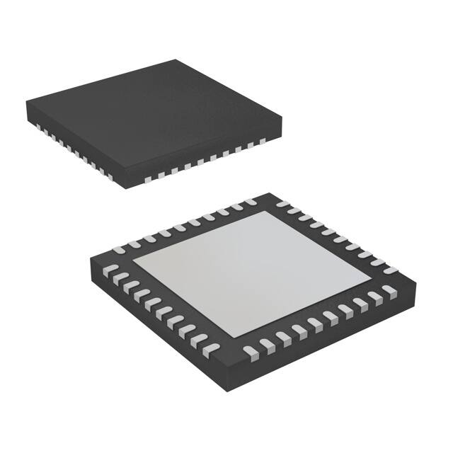


 工商网监
湘ICP备2023018690号
工商网监
湘ICP备2023018690号
