www.ti.com
Table of Contents
User’s Guide
TPS5403 Step-Down Converter Evaluation Module User's
Guide
Table of Contents
1 Introduction.............................................................................................................................................................................2
2 Background.............................................................................................................................................................................2
3 Board Layout...........................................................................................................................................................................2
4 Bench Test Setup Conditions................................................................................................................................................ 4
4.1 Headers Description and Jumper Placement.....................................................................................................................4
4.2 Jumpers and Switches....................................................................................................................................................... 4
5 Power-Up Procedure.............................................................................................................................................................. 4
6 Schematic and Bill of Materials.............................................................................................................................................5
7 Revision History......................................................................................................................................................................6
List of Figures
Figure 3-1. Placement (Top Layer).............................................................................................................................................. 2
Figure 3-2. Board Layout (Top Layer)..........................................................................................................................................3
Figure 3-3. Board Layout (Bottom Layer).................................................................................................................................... 3
Figure 4-1. Headers Description and Jumper Placement............................................................................................................4
Figure 6-1. TPS5403EVM Schematic..........................................................................................................................................5
List of Tables
Table 2-1. Summary of Performance........................................................................................................................................... 2
Table 4-1. Jumpers and Switches................................................................................................................................................4
Table 6-1. TPS5403EVM Bill of Materials....................................................................................................................................6
Trademarks
All trademarks are the property of their respective owners.
SLVU780A – SEPTEMBER 2012 – REVISED NOVEMBER 2021
TPS5403 Step-Down Converter Evaluation Module User's Guide
Submit Document Feedback
Copyright © 2021 Texas Instruments Incorporated
1
�Introduction
www.ti.com
1 Introduction
This document presents the information required to operate the TPS5403 as well as the support documentation
including the schematic and bill of materials.
2 Background
The TPS5403 is designed to provide 1.7-A continuous current with an operational range of 4.5 V to 28 V and an
external set switching frequency ranging from 50 kHz to 1.1 MHz.
As there are many possible options to set the converters, Table 2-1 presents the performance specification
summary for the EVM.
Table 2-1. Summary of Performance
TEST CONDITIONS
PERFORMANCE
VIN = 4.5 V to 28 V
fSW = 300 kHz
(25°C ambient)
Buck: 3.3 V, up to 1.7 A
The evaluation module is designed to provide access to the features of the TPS5403. Some modifications
can be made to this module to test performance at different input and output voltages, current and switching
frequency. Please contact TI Field Applications Group for advice on these matters.
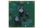
3 Board Layout
Figure 3-1. Placement (Top Layer)
2
TPS5403 Step-Down Converter Evaluation Module User's Guide
SLVU780A – SEPTEMBER 2012 – REVISED NOVEMBER 2021
Submit Document Feedback
Copyright © 2021 Texas Instruments Incorporated
�www.ti.com
Board Layout
Figure 3-2. Board Layout (Top Layer)
Figure 3-3. Board Layout (Bottom Layer)
SLVU780A – SEPTEMBER 2012 – REVISED NOVEMBER 2021
TPS5403 Step-Down Converter Evaluation Module User's Guide
Submit Document Feedback
Copyright © 2021 Texas Instruments Incorporated
3
�Bench Test Setup Conditions
www.ti.com
4 Bench Test Setup Conditions
4.1 Headers Description and Jumper Placement
Figure 4-1. Headers Description and Jumper Placement
Test points:
1. LX, VIN, VOUT
4.2 Jumpers and Switches
Table 4-1. Jumpers and Switches
NO.
JP4
FUNCTION
Switching Frequency
PLACEMENT
Connect JP4 to GND and set the switching frequency to
50 kHz; Leave it open and set switching frequency to 120 kHz;
Connect a resistor to set the switching frequency
COMMENT
See the TPS5405 Monolithic NonSynchronous Step-Down Regulator With
Integrated MOSFET Data Sheet for the
resistor value corresponding to specific
switching frequency.
5 Power-Up Procedure
1. Apply 4.5 V – 28 V to JP1.
2. Apply load to the output connector.
4
TPS5403 Step-Down Converter Evaluation Module User's Guide
SLVU780A – SEPTEMBER 2012 – REVISED NOVEMBER 2021
Submit Document Feedback
Copyright © 2021 Texas Instruments Incorporated
�www.ti.com
Schematic and Bill of Materials
6 Schematic and Bill of Materials
The following pages contain the TPS5403EVM schematic and bill of materials.
Figure 6-1. TPS5403EVM Schematic
SLVU780A – SEPTEMBER 2012 – REVISED NOVEMBER 2021
TPS5403 Step-Down Converter Evaluation Module User's Guide
Submit Document Feedback
Copyright © 2021 Texas Instruments Incorporated
5
�Revision History
www.ti.com
Table 6-1. TPS5403EVM Bill of Materials
ITEM NO.
QTY
DESIGNATOR
VALUE
MANUFACTURER
1
1
C1
0.1 μF
Generic
Capacitor, 0.1 μF, 35 V, Ceramic, X7R,
0603
2
3
C2, C8B, C8C
10 μF
Generic
Capacitor, 10 μF, 35 V, Ceramic, X5R,
0805
3
2
C2A, C8A
220 μF
Rubycon
4
1
C4
10 nF
Generic
Capacitor, 10 nF, 35 V, Ceramic, X7R,
0603
C5
470 pF
Generic
Capacitor, 470 pF, 50 V, Ceramic, X7R,
0603
5
PART NO.
5YXF220MEFC
DESCRIPTION
220 μF/35V 10x12.5
6
1
C6A
2.2 nF
Generic
Capacitor, 2.2 nF, 50 V, Ceramic, X7R,
0603
7
DNI
C6B
100 pF
Generic
Capacitor, 100 pF, 50 V, Ceramic, X7R,
0603
8
1
D1
Comchip
SB240E
Comchip SB240E 2-A/40-V Schottky
Rectifier
9
1
JP4
Mill-Max
Manufacturing Corp.
800-10-064-10-001000
Three Pin Jumper, SIP HEADER 64
POS STRAIGHT PCB
10
1
L1
82 μH
Bourns
RL622-820K-RC
Magnetic-Core Inductor
11
3
R1, R8, R5b1
0
Generic
Resistor, 1%, 1/10W, 0603, SMD
12
1
R3
100 K
Generic
Resistor, 1%, 1/10W, 0603, SMD
13
1
R6
47 K
Generic
Resistor, 1%, 1/10W, 0603, SMD
14
DNI
R5b2
3.8 k
Generic
Resistor, 1%, 1/10W, 0603, SMD
15
2
TP1, TP2
5001
Generic
5001
Keystone Electronics, Test Point, Black
16
3
TP5, TP6, TP7
5002
Generic
5002
Keystone Electronics, Test Point, White
17
1
U1
Texas Instruments
TPS5403
SOIC8
18(1)
1
Sullins Connector
Solutions
SPC02SYAN
SPC02SYAN, CONN JUMPER
SHORTING GOLD FLASH
(1)
Install item 18 on item 8 to the inner side.
7 Revision History
NOTE: Page numbers for previous revisions may differ from page numbers in the current version.
Changes from Revision * (September 2012) to Revision A (November 2021)
Page
• Updated the numbering format for tables, figures, and cross-references throughout the document. ................2
• Updated the user's guide title............................................................................................................................. 2
6
TPS5403 Step-Down Converter Evaluation Module User's Guide
SLVU780A – SEPTEMBER 2012 – REVISED NOVEMBER 2021
Submit Document Feedback
Copyright © 2021 Texas Instruments Incorporated
�IMPORTANT NOTICE AND DISCLAIMER
TI PROVIDES TECHNICAL AND RELIABILITY DATA (INCLUDING DATA SHEETS), DESIGN RESOURCES (INCLUDING REFERENCE
DESIGNS), APPLICATION OR OTHER DESIGN ADVICE, WEB TOOLS, SAFETY INFORMATION, AND OTHER RESOURCES “AS IS”
AND WITH ALL FAULTS, AND DISCLAIMS ALL WARRANTIES, EXPRESS AND IMPLIED, INCLUDING WITHOUT LIMITATION ANY
IMPLIED WARRANTIES OF MERCHANTABILITY, FITNESS FOR A PARTICULAR PURPOSE OR NON-INFRINGEMENT OF THIRD
PARTY INTELLECTUAL PROPERTY RIGHTS.
These resources are intended for skilled developers designing with TI products. You are solely responsible for (1) selecting the appropriate
TI products for your application, (2) designing, validating and testing your application, and (3) ensuring your application meets applicable
standards, and any other safety, security, regulatory or other requirements.
These resources are subject to change without notice. TI grants you permission to use these resources only for development of an
application that uses the TI products described in the resource. Other reproduction and display of these resources is prohibited. No license
is granted to any other TI intellectual property right or to any third party intellectual property right. TI disclaims responsibility for, and you
will fully indemnify TI and its representatives against, any claims, damages, costs, losses, and liabilities arising out of your use of these
resources.
TI’s products are provided subject to TI’s Terms of Sale or other applicable terms available either on ti.com or provided in conjunction with
such TI products. TI’s provision of these resources does not expand or otherwise alter TI’s applicable warranties or warranty disclaimers for
TI products.
TI objects to and rejects any additional or different terms you may have proposed. IMPORTANT NOTICE
Mailing Address: Texas Instruments, Post Office Box 655303, Dallas, Texas 75265
Copyright © 2022, Texas Instruments Incorporated
�