www.ti.com
Table of Contents
User’s Guide
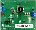
TPS54202H Step-Down Converter Evaluation Module
User's Guide
ABSTRACT
This user's guide contains background information for the TPS54202H as well as support documentation for the
TPS54202HEVM-716 evaluation module (PWR716-001). Also included are the performance specifications, the
schematic, and the bill of materials for the TPS54202HEVM-716.
Table of Contents
1 Introduction.............................................................................................................................................................................2
1.1 Background........................................................................................................................................................................ 2
1.2 Performance Specification Summary.................................................................................................................................2
1.3 Modifications...................................................................................................................................................................... 3
2 Test Setup and Results.......................................................................................................................................................... 4
2.1 Input/Output Connections.................................................................................................................................................. 4
2.2 Efficiency............................................................................................................................................................................5
2.3 Output Voltage Load Regulation........................................................................................................................................ 6
2.4 Output Voltage Line Regulation......................................................................................................................................... 6
2.5 Load Transients..................................................................................................................................................................7
2.6 Output Voltage Ripple........................................................................................................................................................ 8
2.7 Input Voltage Ripple......................................................................................................................................................... 10
2.8 Powering Up.....................................................................................................................................................................11
2.9 Powering Down................................................................................................................................................................ 12
3 Board Layout.........................................................................................................................................................................13
3.1 Layout.............................................................................................................................................................................. 13
4 Schematic and Bill of Materials...........................................................................................................................................15
4.1 Schematic........................................................................................................................................................................ 15
4.2 Bill of Materials.................................................................................................................................................................15
5 Revision History................................................................................................................................................................... 17
List of Figures
Figure 2-1. TPS54202HEVM-716 Efficiency................................................................................................................................5
Figure 2-2. TPS54202HEVM-716 Low Current Efficiency........................................................................................................... 5
Figure 2-3. TPS54202HEVM-716 Load Regulation.....................................................................................................................6
Figure 2-4. TPS54202HEVM-716 Line Regulation......................................................................................................................6
Figure 2-5. TPS54202HEVM-716 Transient Response...............................................................................................................7
Figure 2-6. TPS54202HEVM-716 Output Ripple, IOUT = 2 A.......................................................................................................8
Figure 2-7. TPS54202HEVM-716 Output Ripple, IOUT = 100 mA................................................................................................8
Figure 2-8. TPS54202HEVM-716 Output Ripple, IOUT = 10 mA..................................................................................................9
Figure 2-9. TPS54202HEVM-716 Output Ripple, IOUT = 0 A.......................................................................................................9
Figure 2-10. TPS54202HEVM-716 Input Ripple........................................................................................................................10
Figure 2-11. TPS54202HEVM-716 Startup Relative to VIN .......................................................................................................11
Figure 2-12. TPS54202HEVM-716 Startup Relative to Enable................................................................................................. 11
Figure 2-13. TPS54202HEVM-716 Shutdown Relative to VIN ..................................................................................................12
Figure 2-14. TPS54202HEVM-716 Shutdown Relative to EN...................................................................................................12
Figure 3-1. TPS54202HEVM-716 Top-Side Assembly.............................................................................................................. 13
Figure 3-2. TPS54202HEVM-716 Bottom-Side Layout............................................................................................................. 14
Figure 4-1. TPS54202HEVM-716 Schematic............................................................................................................................ 15
SLVUAP8A – APRIL 2016 – REVISED OCTOBER 2021
Submit Document Feedback
TPS54202H Step-Down Converter Evaluation Module User's Guide
Copyright © 2021 Texas Instruments Incorporated
1
�Trademarks
www.ti.com
List of Tables
Table 1-1. Input Voltage and Output Current Summary...............................................................................................................2
Table 1-2. TPS54202HEVM-716 Performance Specification Summary...................................................................................... 2
Table 1-3. Recommended Component Values............................................................................................................................ 3
Table 2-1. EVM Connectors and Test Points............................................................................................................................... 4
Table 4-1. TPS54202HEVM-716 Bill of Materials...................................................................................................................... 15
Trademarks
All trademarks are the property of their respective owners.
1 Introduction
This user's guide contains background information for the TPS54202H as well as support documentation for the
TPS54202HEVM-716 evaluation module (PWR716-001). Also included are the performance specifications, the
schematic, and the bill of materials for the TPS54202HEVM-716.
1.1 Background
The TPS54202H dc/dc converter is designed to provide up to a 2-A output from an input voltage source of
4.2 V to 28 V. Rated input voltage and output current range for the evaluation module are given in Table 1-1.
This evaluation module is designed to demonstrate the small printed-circuit-board areas that may be achieved
when designing with the TPS54202H regulator. The switching frequency is internally set at a nominal 500 kHz.
The high-side and low-side MOSFETs are incorporated inside the TPS54202H package along with the gatedrive circuitry. The low drain-to-source on resistance of the MOSFETs allow the TPS54202H to achieve high
efficiencies and helps keep the junction temperature low at high output currents. The compensation components
are integrated to the integrated circuit (IC), and an external divider allows for an adjustable output voltage.
Additionally, the TPS54202H provides an adjustable undervoltage lockout input. The absolute maximum input
voltage is 30 V for the TPS54202HEVM-716.
Table 1-1. Input Voltage and Output Current Summary
EVM
Input Voltage Range
Output Current Range
TPS54202HEVM-716
VIN = 4.2 V to 28 V
0 A to 2 A
1.2 Performance Specification Summary
A summary of the TPS54202HEVM-716 performance specifications is provided in Table 1-2. Specifications
are given for an input voltage of VIN = 24 V and an output voltage of 5.0 V, unless otherwise specified. The
TPS54202HEVM-716 is designed and tested for VIN = 4.2 V to 28 V. The ambient temperature is 25°C for all
measurements, unless otherwise noted.
Table 1-2. TPS54202HEVM-716 Performance Specification Summary
Specification
Test Conditions
VIN operating voltage range
MIN
TYP
MAX
4.2
24
28
V
VIN start voltage
4.2
V
VIN stop voltage
3.7
V
Output voltage set point
5
Output current range
VIN = 4.2 V to 28 V
Line regulation
IO = 1 A, VIN = 8 V to 28 V
±0.5%
Load regulation
VIN = 12 V, IO = 0 A to 2 A
±0.5%
IO = 0.5 A to 1.5 A
Load transient response
IO = 1.5 A to 0.5 A
0
V
2
A
Voltage change
–150
mV
Recovery time
150
μs
Voltage change
150
mV
Recovery time
150
μs
Input ripple voltage
IO = 2 A
400
mVPP
Output ripple voltage
IO = 2 A
很抱歉,暂时无法提供与“TPS54202HEVM-716”相匹配的价格&库存,您可以联系我们找货
免费人工找货