www.ti.com
Table of Contents
User’s Guide
TPS54291 Step-Down Converter Evaluation Module User's
Guide
Table of Contents
1 Introduction.............................................................................................................................................................................2
1.1 Description......................................................................................................................................................................... 2
1.2 Applications........................................................................................................................................................................2
1.3 Features............................................................................................................................................................................. 2
2 TPS54291EVM-431 Electrical Performance Specifications................................................................................................ 3
3 Schematic................................................................................................................................................................................4
3.1 Enable Jumpers (JP1 and JP2)......................................................................................................................................... 5
3.2 Error Amplifier Outputs.......................................................................................................................................................5
3.3 Test Point Descriptions.......................................................................................................................................................5
4 Test Setup................................................................................................................................................................................7
4.1 Equipment.......................................................................................................................................................................... 7
4.2 Equipment Setup................................................................................................................................................................8
4.3 Start-Up/Shutdown Procedure........................................................................................................................................... 9
4.4 Output Ripple Voltage Measurement Procedure..............................................................................................................10
4.5 Control Loop Gain and Phase Measurement Procedure................................................................................................. 10
4.6 Equipment Shutdown....................................................................................................................................................... 10
5 TPS54291EVM-431 Typical Performance Data and Characteristic Curves......................................................................11
5.1 Efficiency.......................................................................................................................................................................... 11
5.2 Line and Load Regulation.................................................................................................................................................11
5.3 Switch Node and Output Ripple Voltage.......................................................................................................................... 12
6 EVM Assembly Drawings and Layout.................................................................................................................................13
7 List of Materials.....................................................................................................................................................................16
8 Revision History................................................................................................................................................................... 16
List of Figures
Figure 3-1. TPS54291EVM-431 Schematic.................................................................................................................................4
Figure 4-1. TPS54291EVM-431 Recommended Test Setup....................................................................................................... 8
Figure 4-2. Output Ripple Measurement – Tip and Barrel Using TP3 and TP4 or TP18 and TP19............................................ 9
Figure 4-3. Control Loop Measurement Setup............................................................................................................................ 9
Figure 5-1. TPS54291EVM-431 Efficiency vs Load Current......................................................................................................11
Figure 5-2. TPS54291EVM-431 Output Voltage vs Load Current............................................................................................. 11
Figure 5-3. TPS54291EVM-431 Output Voltage Ripple............................................................................................................ 12
Figure 6-1. TPS54291EVM-431 Component Placement (Viewed from Top).............................................................................13
Figure 6-2. TPS54291EVM-431 Silkscreen (Viewed from Top).................................................................................................13
Figure 6-3. TPS54291EVM-431 Top Copper (Viewed from Top)...............................................................................................14
Figure 6-4. TPS54291EVM-431 Bottom Copper (X-Ray View from Top).................................................................................. 14
Figure 6-5. TPS54291EVM-431 Internal 1 (X-Ray View from Top)........................................................................................... 15
Figure 6-6. TPS54291EVM-431 Internal 2 (X-Ray View from Top)........................................................................................... 15
List of Tables
Table 2-1. TPS54291EVM-431 Electrical and Performance Specifications.................................................................................3
Table 3-1. Test Point Descriptions............................................................................................................................................... 5
Table 7-1. TPS54291EVM-431 Bill of Materials.........................................................................................................................16
Trademarks
All trademarks are the property of their respective owners.
SLVU356A – JANUARY 2010 – REVISED OCTOBER 2021
TPS54291 Step-Down Converter Evaluation Module User's Guide
Submit Document Feedback
Copyright © 2021 Texas Instruments Incorporated
1
�Introduction
www.ti.com
1 Introduction
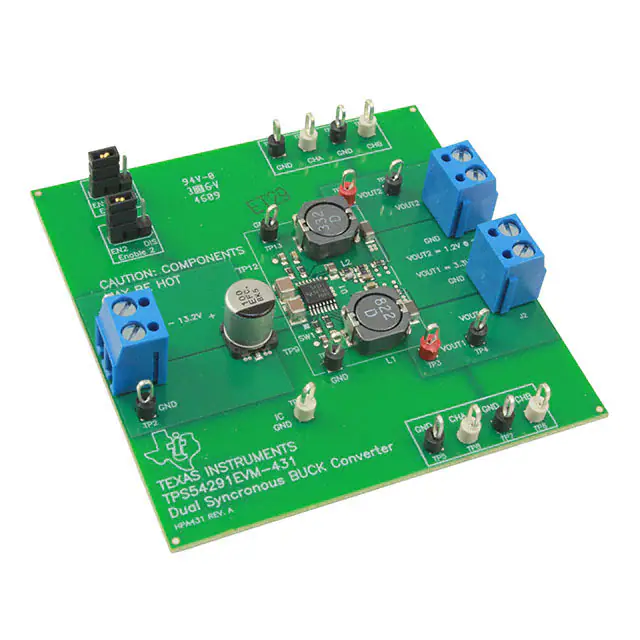
The TPS54291EVM-431 evaluation module (EVM) is a dual synchronous buck converter providing fixed 3.3-V
and 1.2-V outputs at up to 1.5 A and 2.5 A, respectively from a 12-V bus. The EVM is designed to start up from
a single supply, so no additional bias voltages are require for start-up. The module uses the TPS54291 600-kHz
dual synchronous buck converter with integral MOSFETs.
1.1 Description
The TPS54291EVM-431 is designed to use a regulated 12-V (+10% /–20%) bus to produce two regulated power
rails, 3.3 V at 1.5 A and 1.2 V at 2.5 A. TPS54291EVM-431 is designed to demonstrate the TPS54291 in a
typical 12-V bus system while providing a number of test points to evaluate the performance of the TPS54291 in
a given application. The EVM can be modified to other output voltages by changing some of the components.
1.2 Applications
•
•
•
•
•
Non-isolated point-of-load and voltage bus converters
Consumer electronics
LCD TV
Computer peripherals
Digital set top box
1.3 Features
•
•
•
•
•
•
•
•
2
12 V +10% /–20% input range
5.0-V and 3.3-V fixed output voltage, adjustable with resistor change
1.5-A (3.3 V) and 2.5-A (1.2 V) steady state current
600-kHz switching frequency (fixed by TPS54291)
Internal switching MOSFET and external rectifier diode
Double-sided 2 active layer PCB with all components on top side (test point signals routed on internal layers)
Active converter area of 1.1 square inches (0.86" × 1.28")
Convenient test points for probing switching waveforms and non-invasive loop response testing
TPS54291 Step-Down Converter Evaluation Module User's Guide
SLVU356A – JANUARY 2010 – REVISED OCTOBER 2021
Submit Document Feedback
Copyright © 2021 Texas Instruments Incorporated
�www.ti.com
TPS54291EVM-431 Electrical Performance Specifications
2 TPS54291EVM-431 Electrical Performance Specifications
Table 2-1. TPS54291EVM-431 Electrical and Performance Specifications
PARAMETER
NOTES AND CONDITIONS
MIN
NOM
MAX
UNITS
9.6
12
13.2
V
–
2.4
2.6
A
INPUT CHARACTERISTICS
VIN
Input Voltage
IIN
Input Current
VIN = Nom, IOUT = Max
No Load Input Current
VIN = Nom, IOUT = 0 A
Input UVLO
IOUT = Min to Max
VIN_UVLO
–
12
20
mA
4.0
4.2
4.4
V
OUTPUT CHARACTERISTICS
VOUT1
Output Voltage 1
VIN = Nom, IOUT = Nom
3.20
3.30
3.40
V
VOUT2
Output Voltage 2
VIN = Nom, IOUT = Nom
1.15
1.20
1.25
V
Line Regulation
VIN = Min to Max
–
–
1%
Load Regulation
IOUT = Min to Max
–
–
1%
VOUT_ripple
Output Voltage Ripple
VIN = Nom, IOUT = Max
–
–
50
mVpp
IOUT1
Output Current 1
VIN = Min to Max
0
2.5
A
IOUT2
Output Current 2
VIN = Min to Max
0
2.5
A
IOCP1
Output Over Current Channel 1
VIN = Nom, VOUT = VOUT1–5%
1.6
2.0
2.4
A
IOCP2
Output Over Current Channel 2
VIN = Nom, VOUT = VOUT2–5%
3.0
3.6
4.4
A
520
600
720
kHz
SYSTEMS CHARACTERISTICS
FSW
Switching Frequency
ηpk
Peak Efficiency
VIN = Nom
–
88%
–
η
Full Load Efficiency
VIN = Nom, IOUT1 = IOUT1 = Max
–
85%
–
Top
Operating Temperature Range
VIN = Min to Max, IOUT = Min to Max
0
25
60
°C
SLVU356A – JANUARY 2010 – REVISED OCTOBER 2021
TPS54291 Step-Down Converter Evaluation Module User's Guide
Submit Document Feedback
Copyright © 2021 Texas Instruments Incorporated
3
�Schematic
www.ti.com
+
3 Schematic
Figure 3-1. TPS54291EVM-431 Schematic
The schematic is for reference only. See Table 7-1 for specific values.
4
TPS54291 Step-Down Converter Evaluation Module User's Guide
SLVU356A – JANUARY 2010 – REVISED OCTOBER 2021
Submit Document Feedback
Copyright © 2021 Texas Instruments Incorporated
�www.ti.com
Schematic
3.1 Enable Jumpers (JP1 and JP2)
The TPS54291EVM-431 provides separate three pin 100-mil headers and shunts for exercising the TPS54291
Enable functions. Place the JP1 shunt in the left position connects EN1 to ground and turns on Output 1 and
placing the JP2 shunt in the left position connects EN2 to ground and turns on Output 2.
3.2 Error Amplifier Outputs
The output of the TPS54291 transconductance error amplifiers (COMP1 and COMP2) are sensitive to
capacitive loading, including the typical 8-pF to 15-pF capacitance added by an oscilloscope probe. No direct
measurements of these signals should be attempted without using an external buffer to prevent loading of the
control voltage.
3.3 Test Point Descriptions
Table 3-1. Test Point Descriptions
TEST POINT
LABEL
USE
SECTION
TP1
VIN
Monitor Input Voltage
Section 3.3.1
TP2
GND
Ground for Input Voltage
Section 3.3.1
TP3
VOUT1
Monitor VOUT1 Voltage
Section 3.3.2
TP4
GND
Ground for VOUT1 Voltage
Section 3.3.2
TP5
GND
Ground for VOUT1 Channel B Loop Monitoring
Section 3.3.3
TP6
CHB
VOUT1 Channel B for Loop Monitoring
Section 3.3.3
TP7
GND
Ground for VOUT1 Channel A Loop Monitoring
Section 3.3.3
TP8
CHA
VOUT1 Channel B for Loop Monitoring
Section 3.3.3
TP9
SW1
Monitor Switching Node of Channel 1
Section 3.3.4
TP10
GND
Ground for Switch Node of Channel 1
Section 3.3.4
TP11
IC_GND
Monitor IC Ground
Section 3.3.5
TP12
SW2
Monitor Switching Node of Channel 2
Section 3.3.6
TP13
GND
Ground for Switch Node of Channel 2
Section 3.3.6
TP14
CHA
VOUT2 Channel A for Loop Monitoring
Section 3.3.7
TP15
GND
Ground for VOUT2 Channel A Loop Monitoring
Section 3.3.7
TP16
CHB
VOUT2 Channel B for Loop Monitoring
Section 3.3.7
TP17
GND
Ground for VOUT2 Channel B Loop Monitoring
Section 3.3.7
TP18
VOUT2
Monitor VOUT2 Voltage
Section 3.3.8
TP19
GND
Ground for VOUT2 Voltage
Section 3.3.8
3.3.1 Input Voltage Monitoring (TP1 and TP2)
TPS54291EVM-431 provides two test points for measuring the voltage applied to the module. This allows the
user to measure the actual module voltage without losses from input cables and connectors. All input voltage
measurements should be made between TP1 and TP2. To use TP1 and TP2, connect a voltmeter positive
terminal to TP1 and negative terminal to TP2.
3.3.2 Channel 1 Output Voltage Monitoring (TP3 and TP4)
TPS54291EVM-431 provides two test points for measuring the voltage generated by the module. This allows
the user to measure the actual module output voltage without losses from output cables and connectors. All
output voltage measurements should be made between TP3 and TP4. To use TP3 and TP4, connect a voltmeter
positive terminal to TP3 and negative terminal to TP4. For output ripple measurements, TP3 and TP4 allow a
user to limit the ground loop area by using the tip and barrel measurement technique shown in Section 4.2.2.
All output ripple measurements should be made using the tip and barrel measurement. Even this Tip and Barrel
measurement technique increases the measured switch edge noise. For improved output ripple measurement,
measure the output ripple at the output capacitor (C5).
SLVU356A – JANUARY 2010 – REVISED OCTOBER 2021
TPS54291 Step-Down Converter Evaluation Module User's Guide
Submit Document Feedback
Copyright © 2021 Texas Instruments Incorporated
5
�Schematic
www.ti.com
3.3.3 Channel 1 Loop Analysis (TP5, TP6, TP7, and TP8)
The TPS54291EVM-431 contains a 51-Ω series resistor (R1) in the feedback loop to allow for matched
impedance signal injection into the feedback for loop response analysis. An isolation transformer should be
used to apply a small (30 mV or less) signal across R1 through TP6 and TP8. By monitoring the AC injection
level at TP8 and the returned AC level at TP6, the power supply loop response can be determined.
3.3.4 Channel 1 Switching Waveforms (TP9 and TP10)
The TPS54291EVM-431 provides a surface test pad and a local ground connection (TP10) for the monitoring
of the channel 1 power stage switching waveform. Connect an oscilloscope probe to TP9 to monitor the switch
node voltage for channel 1. Test pads are used on the switch nodes to minimize radiated noise from the switch
node.
3.3.5 TPS54291 IC Ground (TP11)
The TPS54291EVM-431 provides a test point for the IC ground. To measure IC pin voltages, connect the ground
of the oscilloscope probe to TP11.
3.3.6 Channel 2 Switching Waveforms (TP12 and TP13)
The TPS54291EVM-431 provides a surface test pad and a local ground connection (TP13) for the monitoring of
the channel 1 power stage switching waveform. Connect an oscilloscope probe to TP12 to monitor the switch
node voltage for channel 1. Test pads are used on the switch nodes to minimize radiated noise from the switch
node.
3.3.7 Channel 2 Loop Analysis (TP14, TP15, TP16, and TP17)
The TPS54291EVM-431 contains a 51-Ω series resistor (R13) in the feedback loop to allow for matched
impedance signal injection into the feedback for loop response analysis. An isolation transformer should be used
to apply a small (30 mV or less) signal across R13 through TP14 and TP16. By monitoring the AC injection level
at TP14 and the returned AC level at TP16, the power supply loop response can be determined.
3.3.8 Output Voltage Monitoring (TP18 and TP19)
The TPS54291EVM-431 provides two test points for measuring the voltage generated by the module. This
allows the user to measure the actual module output voltage without losses from output cables and connector
losses. All output voltage measurements should be made between TP18 and TP19. To use TP18 and TP19,
connect a voltmeter positive terminal to TP18 and negative terminal to TP19. For output ripple measurements,
TP18 and TP19 allow a user to limit the ground loop area by using the tip and barrel measurement technique
shown in Figure 4-2. All output ripple measurements should be made using the tip and barrel measurement.
Even this tip and barrel measurement technique increases the measured switch edge noise. For improved
output ripple measurement, measure the output ripple at the output capacitor (C17).
6
TPS54291 Step-Down Converter Evaluation Module User's Guide
SLVU356A – JANUARY 2010 – REVISED OCTOBER 2021
Submit Document Feedback
Copyright © 2021 Texas Instruments Incorporated
�www.ti.com
Test Setup
4 Test Setup
4.1 Equipment
4.1.1 Voltage Source (VIN)
The input voltage source (VIN) should be a 0-V to 15-V variable DC source capable of 2-A DC. Connect VIN to J1
as shown in Figure 4-2.
4.1.2 Meters
•
•
•
•
A1: 0-Adc to 2-Adc ammeter
V1: VIN, 0-V to 15-V voltmeter
V2: VOUT1, 0-V to 6-V voltmeter
V3: VOUT2, 0-V to 4-V voltmeter
4.1.3 Loads
LOAD1
The Output1 Load (LOAD1) should be an electronic constant current mode load capable of 0 Adc to 1.5 Adc at
3.3 V.
LOAD2
The Output2 Load (LOAD2) should be an electronic constant current mode load capable of 0 Adc to 2.5 Adc at
1.2 V.
4.1.4 Oscilloscope
A Digital or Analog Oscilloscope can be used to measure the ripple voltage on VOUT1 or VOUT2. The
oscilloscope should be set for the following for taking output ripple measurements:
• 1-MΩ impedance
• 20-MHz Bandwidth
• AC coupling
• 1-μs/division horizontal resolution
• 10-mV/division vertical resolution
TP3 and TP4 or TP18 and TP19 can be used to measure the output ripple voltages by placing the oscilloscope
probe tip through TP3 or TP18 and holding the ground barrel to TP4 or TP19 as shown in Figure 4-2. For a
hands free approach, the loop in TP4 or TP19 can be cut and opened to cradle the probe barrel. Using a leaded
ground connection can induce additional noise due to the large ground loop area.
4.1.5 Recommended Wire Gauge
VIN to J1
The connection between the source voltage, VIN, and J1 of HPA431 can carry as much as 5 Adc. The minimum
recommended wire size is AWG #16 with the total length of wire less than four feet (two feet input, two feet
return).
J2 to LOAD1
The power connection between J2 of HPA431 and LOAD1 can carry as much as 1.5 Adc. The minimum
recommended wire size is AWG #18 with the total length of wire less than two feet (two foot output, two foot
return).
J3 to LOAD2
The power connection between J3 of HPA431 and LOAD2 can carry as much as 2.5 Adc. The minimum
recommended wire size is AWG #18 with the total length of wire less than 2two feet (one foot output, one foot
return).
4.1.6 Other
FAN
This evaluation module includes components that can get hot to the touch. Because this EVM is not enclosed to
allow probing of circuit nodes, a small fan capable of 200lfm to 400 lfm is recommended to reduce component
surface temperatures to prevent user injury. The EVM should not be left unattended while powered. The EVM
should not be probed while the fan is not running.
SLVU356A – JANUARY 2010 – REVISED OCTOBER 2021
TPS54291 Step-Down Converter Evaluation Module User's Guide
Submit Document Feedback
Copyright © 2021 Texas Instruments Incorporated
7
�Test Setup
www.ti.com
4.2 Equipment Setup
Shown in Figure 4-1 is the basic recommended test setup to evaluate the TPS54291EVM-431. Note that
although the return for J1, J2, and JP3 is the same system ground, the connections should remain separate as
shown in Figure 4-1.
4.2.1 Procedure
1. Working at an ESD workstation, make sure that any wrist straps, bootstraps, or mats are connected
referencing the user to earth ground before power is applied to the EVM. An electrostatic smock and safety
glasses should also be worn.
2. Prior to connecting the DC input source, VIN, it is advisable to limit the source current from VIN to 2.0-A
maximum. Make sure VIN is initially set to 0 V and connected as shown in Figure 4-1.
3. Connect the ammeter A1 (0-A to 5-A range) between VIN and J1 as shown in Figure 4-1.
4. Connect voltmeter V1 to TP1 and TP2 as shown in Figure 4-1.
5. Connect LOAD1 to J2 as shown in Figure 4-1. Set LOAD1 to constant current mode to sink 0 Adc before VIN
is applied.
6. Connect voltmeter V2 across TP3 and TP4 as shown in Figure 4-1.
7. Connect LOAD2 to J3 as shown in Figure 4-1. Set LOAD2 to constant current mode to sink 0 Adc before VIN
is applied.
8. Connect voltmeter V3 across TP18 and TP19 as shown in Figure 4-1.
9. Place a fan as shown in Figure 4-2 and turn it on, making sure air is flowing across the EVM.
4.2.2 Diagram
FAN
Oscilloscope
1MW, AC
20mV / div
20MHz
+
-
See Tip and Barrel
Measurement for
Vout ripple
V3
+
+
-
LOAD2
1.2V @
2.5A
A1
-
-
-
VVIN
+
V1
+
LOAD1
3.3V @
1.5A
-
+
V2
Figure 4-1. TPS54291EVM-431 Recommended Test Setup
8
TPS54291 Step-Down Converter Evaluation Module User's Guide
SLVU356A – JANUARY 2010 – REVISED OCTOBER 2021
Submit Document Feedback
Copyright © 2021 Texas Instruments Incorporated
�www.ti.com
Test Setup
Metal Ground Barrel
Probe Tip
TP3 /
TP4 /
TP18
TP19
Tip and Barrel Vout ripple
measurement
Figure 4-2. Output Ripple Measurement – Tip and Barrel Using TP3 and TP4 or TP18 and TP19
Network
Analyzer
FAN
Isolation
Transformer
+
V3
+
+
A1
-
-
-
VVIN
+
V1
LOAD2
1.2V @
2.5A
+
LOAD1
3.3V @
1.5A
-
+
V2
Figure 4-3. Control Loop Measurement Setup
4.3 Start-Up/Shutdown Procedure
1.
2.
3.
4.
Increase VIN from 0 Vdc to 12 Vdc.
Vary LOAD1 from 0 Adc to 1.5 Adc.
Vary LOAD2 from 0 Adc to 2.5 Adc.
Vary VIN from 9.6 Vdc to 13.2 Vdc.
SLVU356A – JANUARY 2010 – REVISED OCTOBER 2021
TPS54291 Step-Down Converter Evaluation Module User's Guide
Submit Document Feedback
Copyright © 2021 Texas Instruments Incorporated
9
�Test Setup
www.ti.com
5. Decrease VIN to 0 Vdc.
6. Decrease LOAD1 to 0 A.
7. Decrease LOAD2 to 0 A.
4.4 Output Ripple Voltage Measurement Procedure
See Section 5.3 for more information on measuring output ripple.
1.
2.
3.
4.
5.
6.
7.
8.
9.
Increase VIN from 0 Vdc to 12 Vdc.
Adjust LOAD1 to desired load between 0 Adc and 1.5 Adc.
Adjust LOAD2 to desired load between 0 Adc and 2.5 Adc.
Adjust VIN to desired load between 9.6 Vdc and 13.2 Vdc.
Connect an oscilloscope probe to TP3 and TP4 or TP18 and TP19 as shown in Figure 4-2.
Measure output ripple.
Decrease VIN to 0 Vdc.
Decrease LOAD1 to 0 A.
Decrease LOAD2 to 0 A.
4.5 Control Loop Gain and Phase Measurement Procedure
1.
2.
3.
4.
5.
6.
7.
8.
9.
10.
Connect a 1-kHz to 1-MHz isolation transformer to TP6 and TP8 as shown in Figure 4-3
Connect the input signal amplitude measurement probe (Channel A) to TP8 as shown in Figure 4-3.
Connect output signal amplitude measurement probe (Channel B) to TP6 as shown in Figure 4-3.
Connect ground lead of Channel A and Channel B to TP5 and TP7 as shown in Figure 4-3.
Inject 30-mV or less signal across R1 through an isolation transformer.
Sweep frequency from 1 kHz to 1 MHz with 1-0Hz or lower post filter.
æ C hannelB ö
20 ´ LOG ç
÷
è ChannelA ø .
Control loop gain can be measured by
The control loop phase is measured by the phase difference between Channel A and Channel B.
The control loop for Channel 2 can be measured by making the following substitutions:
a. Change TP6 to TP16.
b. Change TP8 to TP14.
c. Change TP5 to TP17.
d. Change TP7 to TP15.
Disconnect the isolation transformer before making any other measurements (signal injection into feedback
can interfere with the accuracy of other measurements).
4.6 Equipment Shutdown
1.
2.
3.
4.
5.
10
Shut down the oscilloscope.
Shut down VIN.
Shut down LOAD1.
Shut down LOAD2.
Shut down the fan.
TPS54291 Step-Down Converter Evaluation Module User's Guide
SLVU356A – JANUARY 2010 – REVISED OCTOBER 2021
Submit Document Feedback
Copyright © 2021 Texas Instruments Incorporated
�www.ti.com
TPS54291EVM-431 Typical Performance Data and Characteristic Curves
5 TPS54291EVM-431 Typical Performance Data and Characteristic Curves
Figure 5-1 through Figure 5-3 present typical performance curves for the TPS54291EVM-431. Since actual
performance data can be affected by measurement techniques and environmental variables, these curves are
presented for reference and can differ from actual field measurements.
5.1 Efficiency
100
90
8V
8V
12 V
95
12 V
85
14 V
85
η - Efficiency - %
η - Efficiency - %
90
80
75
80
14 V
75
70
70
65
65
60
0
0.2
0.4
0.6
0.8
1
1.2
ILOAD - Load Current - A
1.4
60
1.6
0
0.5
1
1.5
2
ILOAD - Load Current - A
2.5
3
VIN = 9.6-13.2V, VOUT1 = 3.3V IOUT1 = 0-1.5A, VOUT2 = 1.2V IOUT2 = 0-2.5A
Figure 5-1. TPS54291EVM-431 Efficiency vs Load Current
5.2 Line and Load Regulation
1.212
3.35
3.33
14 V
VO - Output Voltage - V
VO - Output Voltage - V
12 V
3.31
8V
3.29
1.206
14 V
1.2
12 V
8V
1.194
3.27
3.25
1.188
0
0.2
0.4
0.6
0.8
1
1.2
ILOAD - Load Current - A
1.4
1.6
0
0.5
1
1.5
2
ILOAD - Load Current - A
2.5
3
VIN = 9.6 V–13.2 V, VOUT1 = 3.2 V IOUT1 = 0 A–1.5 A, VOUT2 = 1.2 V IOUT2 = 0 A–2.5 A
Figure 5-2. TPS54291EVM-431 Output Voltage vs Load Current
SLVU356A – JANUARY 2010 – REVISED OCTOBER 2021
TPS54291 Step-Down Converter Evaluation Module User's Guide
Submit Document Feedback
Copyright © 2021 Texas Instruments Incorporated
11
�TPS54291EVM-431 Typical Performance Data and Characteristic Curves
www.ti.com
5.3 Switch Node and Output Ripple Voltage
VIN = 13.2 V, VOUT1 = 3.3 A, IOUT2 = 1.2 V IOUT2 = 2.5 A
Ch1: TP3 (VOUT1), Ch2: TP18 (VOUT2), Ch3: TP9 (SW1), Ch4: TP12 (SW2)
Figure 5-3. TPS54291EVM-431 Output Voltage Ripple
12
TPS54291 Step-Down Converter Evaluation Module User's Guide
SLVU356A – JANUARY 2010 – REVISED OCTOBER 2021
Submit Document Feedback
Copyright © 2021 Texas Instruments Incorporated
�www.ti.com
EVM Assembly Drawings and Layout
6 EVM Assembly Drawings and Layout
Figure 6-1 through Figure 6-6 show the designs of the TPS54291EVM-431 printed circuit board. The EVM has
been designed using a 4-layer, 2-oz copper-clad circuit board 3.0 inch × 3.0 inch with all components in a
0.86-inch × 1.28-inch active area on the top side and all active traces to the top and bottom layers to allow the
user to easily view, probe, and evaluate the TPS54291 control IC in a practical double-sided application. Moving
components to both sides of the PCB or using additional internal layers can offer additional size reduction for
space constrained systems.
Figure 6-1. TPS54291EVM-431 Component Placement (Viewed from Top)
Figure 6-2. TPS54291EVM-431 Silkscreen (Viewed from Top)
SLVU356A – JANUARY 2010 – REVISED OCTOBER 2021
TPS54291 Step-Down Converter Evaluation Module User's Guide
Submit Document Feedback
Copyright © 2021 Texas Instruments Incorporated
13
�EVM Assembly Drawings and Layout
www.ti.com
Figure 6-3. TPS54291EVM-431 Top Copper (Viewed from Top)
Figure 6-4. TPS54291EVM-431 Bottom Copper (X-Ray View from Top)
14
TPS54291 Step-Down Converter Evaluation Module User's Guide
SLVU356A – JANUARY 2010 – REVISED OCTOBER 2021
Submit Document Feedback
Copyright © 2021 Texas Instruments Incorporated
�www.ti.com
EVM Assembly Drawings and Layout
Figure 6-5. TPS54291EVM-431 Internal 1 (X-Ray View from Top)
Figure 6-6. TPS54291EVM-431 Internal 2 (X-Ray View from Top)
SLVU356A – JANUARY 2010 – REVISED OCTOBER 2021
TPS54291 Step-Down Converter Evaluation Module User's Guide
Submit Document Feedback
Copyright © 2021 Texas Instruments Incorporated
15
�List of Materials
www.ti.com
7 List of Materials
Table 7-1 lists the EVM components as configured according to the schematic shown in Figure 3-1.
Table 7-1. TPS54291EVM-431 Bill of Materials
QTY
REFDES
VALUE
DESCRIPTION
SIZE
PART NUMBER
MFR
1
C1
100 μF
Capacitor, Aluminum, 25 V, ±20%
0.328 × 0.390 inch
EEEFC1E101P
Panasonic
1
C12
4.7 μF
Capacitor, Ceramic, 10 V, X5R, 20%
0805
Std
Std
2
C2, C14
22 μF
Capacitor, Ceramic, 6.3 V, X5R, 20%
1206
C3216X5R0J226M
TDK
2
C3, C13
470 pF
Capacitor, Ceramic, 25 V, X7R, 20%
0603
Std
Std
2
C4, C11
0.047 μF
Capacitor, Ceramic, 25 V, X7R, 20%
0603
Std
Std
2
C5, C10
10 μF
Capacitor, Ceramic, 25 V, X5R, 20%
1210
C3225X5R1E106M
TDK
1
C6
1.8 nF
Capacitor, Ceramic, 25 V, X7R, 20%
0603
Std
Std
1
C7
15 pF
Capacitor, Ceramic, 25 V, C0G, 20%
0603
Std
Std
1
C8
47 pF
Capacitor, Ceramic, 25 V, C0G, 20%
0603
Std
Std
1
C9
1.2 nF
Capacitor, Ceramic, 25 V, X7R, 20%
0603
Std
Std
3
J1, J2, J3
ED1609-ND
Terminal Block, 2-pin, 15-A, 5.1 mm
0.40 × 0.35 inch
ED120/2DS
OST
2
JP1, JP2
PEC03SAAN
Header, 3-pin, 100-mil spacing
0.100 inch × 3
PEC03SAAN
Sullins
1
L1
8.2 μH
Inductor, SMT, 4.38 A, 20 mΩ
0.402 × 0.394 inch
MSS1048-822L
Coilcraft
1
L2
3.3 μH
Inductor, SMT, 4.38 A, 20 mΩ
0.402 × 0.394 inch
MSS1048-332L
Coilcraft
2
R1, R8
51
Resistor, Chip, 1/16W, 5%
0603
Std
Std
1
R10
40.2 k
Resistor, Chip, 1/16W, 1%
0603
Std
Std
2
R2, R11
10
Resistor, Chip, 1/16W, 5%
0603
Std
Std
2
R3, R12
20.5 k
Resistor, Chip, 1/16W, 1%
0603
Std
Std
1
R4
6.49 k
Resistor, Chip, 1/16W, 1%
0603
Std
Std
2
R5, R9
0
Resistor, Chip, 1/16W, 5%
0603
Std
Std
1
R6
53.6 k
Resistor, Chip, 1/16W, 1%
0603
Std
Std
1
R7
18.7 k
Resistor, Chip, 1/16W, 1%
0603
Std
Std
3
TP1, TP3, TP18
5010
TP2, TP4, TP5, TP7,
TP10, TP13, TP15
Test Point, Red, Thru Hole
0.125 × 0.125 inch
5010
Keystone
9
TP17, TP19, TP6,
TP8, TP11, TP14
5011
Test Point, Black, Thru Hole
0.125 × 0.125 inch
5011
Keystone
5
TP16
5012
Test Point, White, Thru Hole
0.125 × 0.125 inch
5012
Keystone
0
TP9, TP12
None
Test point, 40 mil SMT
None
None
None
1
U1
TPS54291PWP
IC, 2.5-A/1.5-A, 600-Hz, Dual Output Fully
Synchronous Buck Converter W/Integrated
FET
CSP
TPS54291PWP
TI
2
—
Shunt, 100-mil, Black
0.100
929950-00
3M
1
—
PCB, 3 inch × 3 inch × 0.063 inch
HPA431
Any
8 Revision History
NOTE: Page numbers for previous revisions may differ from page numbers in the current version.
Changes from Revision * (January 2010) to Revision A (October 2021)
Page
• Updated the numbering format for tables, figures, and cross-references throughout the document. ................2
• Updated the user's guide title............................................................................................................................. 2
• Edited the user's guide for clarity........................................................................................................................2
16
TPS54291 Step-Down Converter Evaluation Module User's Guide
SLVU356A – JANUARY 2010 – REVISED OCTOBER 2021
Submit Document Feedback
Copyright © 2021 Texas Instruments Incorporated
�IMPORTANT NOTICE AND DISCLAIMER
TI PROVIDES TECHNICAL AND RELIABILITY DATA (INCLUDING DATA SHEETS), DESIGN RESOURCES (INCLUDING REFERENCE
DESIGNS), APPLICATION OR OTHER DESIGN ADVICE, WEB TOOLS, SAFETY INFORMATION, AND OTHER RESOURCES “AS IS”
AND WITH ALL FAULTS, AND DISCLAIMS ALL WARRANTIES, EXPRESS AND IMPLIED, INCLUDING WITHOUT LIMITATION ANY
IMPLIED WARRANTIES OF MERCHANTABILITY, FITNESS FOR A PARTICULAR PURPOSE OR NON-INFRINGEMENT OF THIRD
PARTY INTELLECTUAL PROPERTY RIGHTS.
These resources are intended for skilled developers designing with TI products. You are solely responsible for (1) selecting the appropriate
TI products for your application, (2) designing, validating and testing your application, and (3) ensuring your application meets applicable
standards, and any other safety, security, regulatory or other requirements.
These resources are subject to change without notice. TI grants you permission to use these resources only for development of an
application that uses the TI products described in the resource. Other reproduction and display of these resources is prohibited. No license
is granted to any other TI intellectual property right or to any third party intellectual property right. TI disclaims responsibility for, and you
will fully indemnify TI and its representatives against, any claims, damages, costs, losses, and liabilities arising out of your use of these
resources.
TI’s products are provided subject to TI’s Terms of Sale or other applicable terms available either on ti.com or provided in conjunction with
such TI products. TI’s provision of these resources does not expand or otherwise alter TI’s applicable warranties or warranty disclaimers for
TI products.
TI objects to and rejects any additional or different terms you may have proposed. IMPORTANT NOTICE
Mailing Address: Texas Instruments, Post Office Box 655303, Dallas, Texas 75265
Copyright © 2022, Texas Instruments Incorporated
�