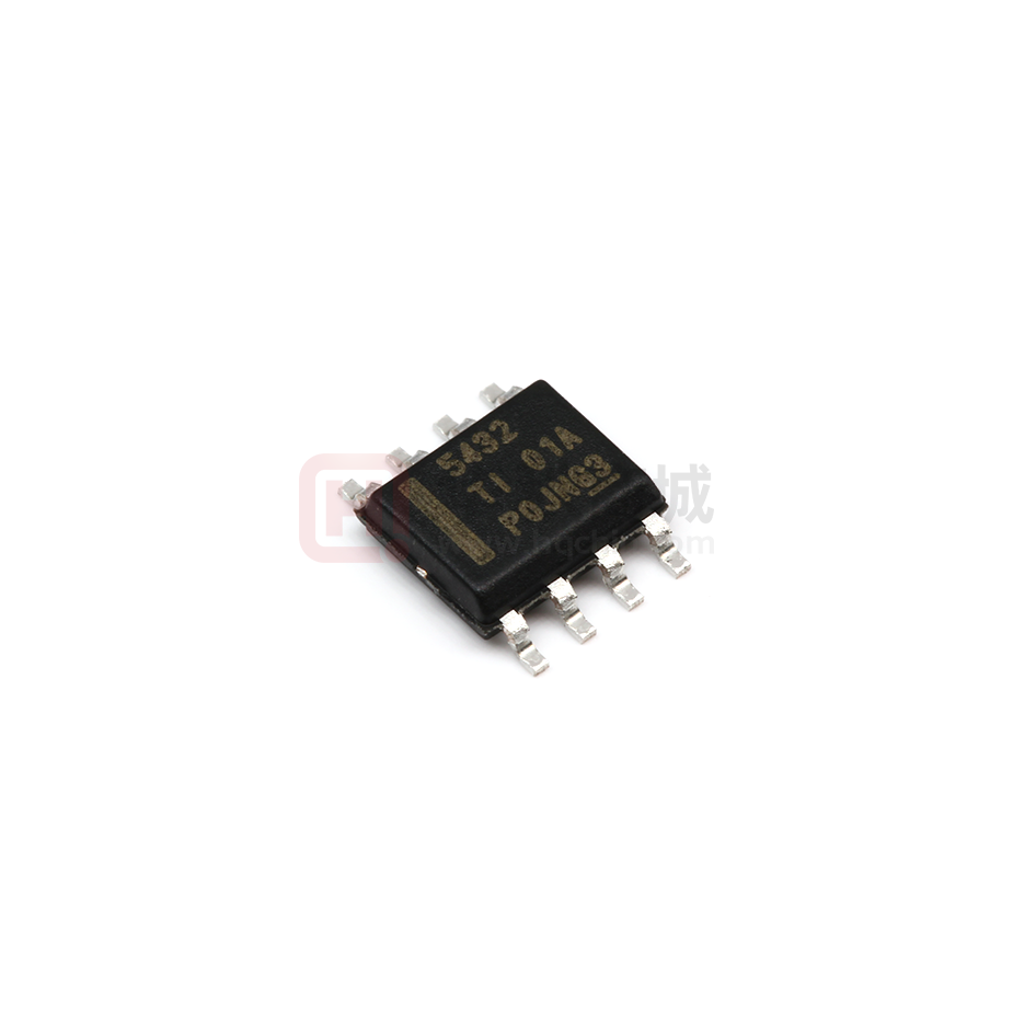
TPS5432
www.ti.com
SLVSB89A – MARCH 2012 – REVISED OCTOBER 2012
2.95V to 6V Input, 3A Output, 700kHz Synchronous Step Down Converter
Check for Samples: TPS5432
FEATURES
DESCRIPTION
•
The TPS5432 is a 6V, 3A, low Iq, current mode,
synchronous monolithic buck converter with
integrated MOSFETs. The TPS5432 enables small
designs by integrating the MOSFETs, implementing
current mode control to reduce external component
count, reducing inductor size by 700kHz switching
frequency. SOIC-8 package with exposed thermal
pad provides both thermally enhanced solution and
easy to use.
1
2
•
•
•
•
•
•
•
•
•
•
Two 70mΩ (typical) MOSFETs for 3A
Continuous Output Current
Current Mode Control With External
Compensation
700kHz Switching Frequency
360µA no Load Quiescent Operating Current
(no switching)
0.808V Internal Voltage Reference
±2.0% Reference Accuracy at 25°C
±3.0% Reference Accuracy Over Temperature
Range –40°C~125°C
Stable Operation With Ceramic Output
Capacitor
Adjustable Slow Start
Cycle by Cycle Current Limit, and Frequency
Fold Back Protection
Thermally Enhanced 8-Pin SOIC (DDA)
Package
The TPS5432 provides accurate regulation for a
variety of loads with an accurate 3.0% voltage
reference over temperature.
Efficiency is maximized through the integrated 70mΩ
MOSFETs and 360μA typical supply current. Using
the enable pin, shutdown supply current is reduced to
2 µA by entering a shutdown mode.
The output voltage startup ramp is controlled by the
slow start pin. A ceramic capacitor at this pin can
easily adjust the slow start time.
Frequency fold back and thermal shutdown protects
the device during an over-current condition.
APPLICATIONS
•
•
Consumer Applications such as DTV, Set Top
Boxes, LCD displays, CPE
Low-Voltage Point-of-Load Regulations for
SoC, CPU, DSP
100
SIMPLIFIED SCHEMATIC
90
2
VIN
BOOT
Cin
10 mF
10 V
TPS5432
7
6
Rc
4.99 kW
Cc
3.3 nF
95
8
1
LO
0.1 mF
10 V
3.3 mH
PH 3
85
1.2 V@3 A
CO
22 mFx2
EN
COMP
CBOOT
VSENSE
5
R1
10 kW
R2
20 kW
SS
GND
Efficiency - %
INPUT
3-6 V
4
Cff
390 pF
80
75
70
Vin = 5 V, Vout = 1.2 V
Vin = 3.3 V, Vout = 1.2 V
Vin = 5 V, Vout = 1.8 V
Vin = 3.3 V, Vout = 1.8 V
Vin = 5 V, Vout = 3.3 V
65
60
55
50
0
500
1000
1500
2000
Load Current - mA
2500
3000
Css
0.01 mF
1
2
Please be aware that an important notice concerning availability, standard warranty, and use in critical applications of
Texas Instruments semiconductor products and disclaimers thereto appears at the end of this data sheet.
PowerPAD is a trademark of Texas Instruments.
PRODUCTION DATA information is current as of publication date.
Products conform to specifications per the terms of the Texas
Instruments standard warranty. Production processing does not
necessarily include testing of all parameters.
Copyright © 2012, Texas Instruments Incorporated
�TPS5432
SLVSB89A – MARCH 2012 – REVISED OCTOBER 2012
www.ti.com
These devices have limited built-in ESD protection. The leads should be shorted together or the device placed in conductive foam
during storage or handling to prevent electrostatic damage to the MOS gates.
PIN CONFIGURATION
SO-8 WITH THERMAL PAD
(TOP VIEW)
BOOT
1
VIN
2
8
SS
7
EN
Thermal
Pad
PH
3
6
COMP
GND
4
5
VSENSE
PIN FUNCTIONS
PIN
DESCRIPTION
NAME
NUMBER
BOOT
1
A bootstrap cap is required between BOOT and PH. If the voltage on this cap is below the minimum
required by the output device, the output is forced to switch off until the cap is refreshed.
COMP
6
Error amplifier output, and input to the output switch current comparator. Connect frequency compensation
to this pin.
EN
7
This pin has an internal pull up which enables switching if left open. To disable switching and reduce
quiescent current, this pin must be pulled to ground.
GND
4
Ground. This pin should be electrically connected directly to the thermal pad under the IC
PH
3
The source of the internal high side power MOSFET, and drain of the internal low side (synchronous)
rectifier MOSFET.
SS
8
Slow start time setting. An external capacitor connected to this pin sets the output rise time
THERMAL PAD
9
GND pin should be connected to the exposed thermal pad for proper operation. This thermal pad should
be connected to any internal PCB ground plane using multiple vias for good thermal performance.
VIN
2
Supplies the control circuitry and switches of the power converter. The range is 2.95V to 6V.
VSENSE
5
Inverting node of the gm error amplifier.
ORDERING INFORMATION (1)
PACKAGE (2)
Tj
–40°C to 125°C
(1)
(2)
(3)
2
8-pin SOIC PowerPAD™
(3)
ORDERABLE PART NUMBER
Tube
TPS5432DDA
Tape and Reel
TPS5432DDAR
For the most current package and ordering information, see the Package Option Addendum at the end of this document, or see the TI
web site at www.ti.com.
Package drawings, thermal data, and symbolization are available at www.ti.com/packaging.
All package options have Cu NIPDAU lead/ball finish.
Submit Documentation Feedback
Copyright © 2012, Texas Instruments Incorporated
Product Folder Links: TPS5432
�TPS5432
www.ti.com
SLVSB89A – MARCH 2012 – REVISED OCTOBER 2012
ABSOLUTE MAXIMUM RATING (1)
VALUE
MIN
Input voltage
MAX
VIN
–0.3
7
EN
–0.3
3.6
BOOT
PH + 7
VSENSE
–0.3
3
COMP
–0.3
3
SS
–0.3
3
BOOT-PH
Output voltage
Sink current
–0.6
–2
(2)
V
10
100
COMP
100
SS
100
Electrostatic discharge (CDM) QSS 009-147 (JESD22-C101B.01)
(1)
7
EN
Electrostatic discharge (HBM) QSS 009-105 (JESD22-A114A) (2)
Temperature
V
7
PH
PH 10 ns Transient
Source current
UNIT
µA
µA
2
kV
500
V
TJ
–40
150
Tstg
–65
150
°C
Stresses beyond those listed under absolute maximum ratings may cause permanent damage to the device. These are stress ratings
only, and functional operation of the device at these or any other conditions beyond those indicated under ELECTRICAL
SPECIFICATIONS is not implied. Exposure to absolute-maximum-rated conditions for extended periods may affect device reliability.
The human body model is a 100-pF capacitor discharge through a 1.5-kΩ resistor into each pin. The machine model is a 200-pF
capacitor discharged directly into each pin.
THERMAL INFORMATION
THERMAL METRIC (1)
TPS5432
DDA (8 PINS)
θJA
Junction-to-ambient thermal resistance
42.1
θJCtop
Junction-to-case (top) thermal resistance
50.9
θJB
Junction-to-board thermal resistance
31.8
ψJT
Junction-to-top characterization parameter
ψJB
Junction-to-board characterization parameter
13.5
θJCbot
Junction-to-case (bottom) thermal resistance
7.1
5
UNITS
°C/W
spacer
(1)
For more information about traditional and new thermal metrics, see the IC Package Thermal Metrics application report, SPRA953.
spacer
Submit Documentation Feedback
Copyright © 2012, Texas Instruments Incorporated
Product Folder Links: TPS5432
3
�TPS5432
SLVSB89A – MARCH 2012 – REVISED OCTOBER 2012
www.ti.com
ELECTRICAL CHARACTERISTICS
The Electrical Ratings specified in this section apply to all specifications in this document, unless otherwise noted. These
specifications are interpreted as conditions that do not degrade the parametric or functional specifications of the device for the
life of the product containing it. Test Conditions: TJ = –40°C to 125°C, VIN = 2.95 to 6V, (unless otherwise noted)
PARAMETERS
CONDITIONS
MIN
TYP
MAX
UNIT
SUPPLY VOLTAGE
Vin
2.95
6
V
2
5
µA
No load, Vin = 5 V, no switching, Vsense = 1 V, 25°C
360
575
µA
Rising Vin
2.6
2.8
V
Iq shutdown
EN = 0V, 25°C, 2.95 V < Vin < 6 V
Iq operating
VIN UVLO
Input UVLO threshold
Input UVLO hysteresis
0.2
V
ENABLE
Enable threshold
Rising
0.984
1.23
Enable threshold
Falling
0.952
1.19
Input current
Enable threshold +50 mv
–4.6
Enable threshold –50 mv
–1.2
1.47
V
µA
VOLTAGE REFERENCE
Reference
2.95 V < Vin < 6 V, TJ = 25°C
0.792
0.808
0.824
V
2.95 V < Vin < 6 V, –40°C < TJ < +125°C
0.784
0.808
0.832
V
MOSFET
H.S switch resistance
BOOT-PH = 5 V, TJ = 25°C
62
86
mΩ
L.S switch resistance
Vin = 5 V, TJ = 25°C
73
103
mΩ
H.S switch resistance
BOOT-PH = 2.95 V, TJ = 25°C
88
114
mΩ
L.S switch resistance
Vin = 2.95 V, TJ = 25°C
94
128
mΩ
ERROR AMPLIFIER
Error amp transconductance (gm)
–2 µA < ICOMP < 2 µA, V(COMP) = 1 V
Error amp transconductance (gm) during soft start
–2 µA < ICOMP < 2 µA,V(COMP) = 1 V, Vsense = 0.3 V
Error amp source/sink
V(COMP) = 1 V, 100 mV overdrive
COMP to Iph gm
245
µmho
70
µmho
±20
µA
Vin = 5 V, Iph1 = (0.5 or 1A) and Iph2 = 3 A
15
A/V
Vsense voltage for Fs foldback
50% frequency
0.4
V
Vsense voltage for Fs foldback
25% frequency
0.2
V
FREQUENCY FOLDBACK vs. VSENSE
CURRENT LIMIT
I max High side FET
Vin = 3.3 V, duty cycle = 100%
I max Low side FET
3.8
5.7
0.8
1.8
7
A
A
155
170
C
15
C
THERMAL SHUTDOWN
Thermal Shutdown
OT Hysteresis
SWITCHING FREQUENCY
Switching frequency
520
700
880
kHz
120
150
ns
PH (PH PIN)
Minimum on time
Vin = 5 V; Measured at 50% points on PH, Iout = 3 A
Minimum off time
Prior to skipping off pulses, BOOT-PH = 2.95 V, Iout = 3 A
60
ns
Rise/Fall time
Vin = 5 V, Io = 0 A
1.5
V/ns
Rise/Fall time
Vin = 5 V, Io = 3 A
1.5
V/ns
BOOT
Boot recharge FET resistance
Vin = 5 V
15
Ω
Boot UVLO
Vin = 2.95 V
2.1
V
2
μA
SLOW START TIME
Charge current
4
Vss = 0.4 V
Submit Documentation Feedback
Copyright © 2012, Texas Instruments Incorporated
Product Folder Links: TPS5432
�TPS5432
www.ti.com
SLVSB89A – MARCH 2012 – REVISED OCTOBER 2012
TYPICAL CHARACTERISTICS CURVES
HIGH SIDE & LOW SIDE Rdson
vs
JUNCTION TEMPERATURE
FREQUENCY
vs
JUNCTION TEMPERATURE
750
120
110
HSF, VI = 3.3 V
LSF, VI = 5 V
100
90
VI =5 V
LSF, VI = 3.3 V
fsw - Switching Frequency - kHz
Rdson - Static Drain-Source On Resistance - mW
130
HSF, VI = 5 V
80
70
60
710
690
670
50
40
-50
-25
0
25
50
75
100
TJ - Junction Temperature - °C
125
650
-50
150
-25
0
25
50
75
100
TJ - Junction Temperature - °C
Figure 1.
Figure 2.
HIGH SIDE CURRENT LIMIT THRESHOLD
vs
JUNCTION TEMPERATURE
VOLTAGE REFERENCE
vs
JUNCTION TEMPERATURE
8
125
150
125
150
0.840
VI = 3.3 V
7
Vref - Voltage Reference - V
IcI - High Side Current Limit Threshold - A
730
VI = 5 V
6
VI = 3.3 V
5
0.820
0.800
4
3
-50
-25
0
25
50
75
100
TJ - Junction Temperature - °C
125
150
0.780
-50
Figure 3.
-25
0
25
50
75
100
TJ - Junction Temperature - °C
Figure 4.
Submit Documentation Feedback
Copyright © 2012, Texas Instruments Incorporated
Product Folder Links: TPS5432
5
�TPS5432
SLVSB89A – MARCH 2012 – REVISED OCTOBER 2012
www.ti.com
TYPICAL CHARACTERISTICS CURVES (continued)
SWITCHING FREQUENCY
vs
VSENSE
EA TRANSCONDUCTANCE
vs
JUNCTION TEMPERATURE
100
290
EA - Transconductance - mA/V
Nominal Switching Frequency - %
TJ = 25°C
75
Vsense Falling
Vsense Rising
50
25
VI = 3.3 V
270
250
230
210
190
0
0
0.1
0.2
0.3
0.4
0.5
VSENSE - V
0.6
0.7
170
-50
0.8
-25
0
25
50
75
100
TJ - Junction Temperature - °C
125
Figure 5.
Figure 6.
EA TRANSCONDUCTANCE (SLOW START)
vs
JUNCTION TEMPERATURE
SLOW START CHARGE CURRENT
vs
JUNCTION TEMPERATURE
150
2.6
105
VI = 3.3 V
100
ISS - SS Charge Current - mA
EA - Transconductance - mA/V
95
90
85
80
75
70
2.5
2.4
2.3
65
60
55
-50
-25
0
25
50
75
100
TJ - Junction Temperature - °C
125
150
2.2
-50
Figure 7.
6
-25
0
25
50
75
100
TJ - Junction Temperature - °C
125
150
Figure 8.
Submit Documentation Feedback
Copyright © 2012, Texas Instruments Incorporated
Product Folder Links: TPS5432
�TPS5432
www.ti.com
SLVSB89A – MARCH 2012 – REVISED OCTOBER 2012
TYPICAL CHARACTERISTICS CURVES (continued)
INPUT VOLTAGE UVLO THRESHOLD
vs
JUNCTION TEMPERATURE
SHUTDOWN SUPPLY CURRENT
vs
JUNCTION TEMPERATURE
4
2.9
VI = 3.3 V; EN = 0 V
Isd - Shutdown Quiescent Current - mA
2.8
VI - UVLO Threshold - V
UVLO Start switching
2.7
2.6
UVLO Stop switching
2.5
2.4
2.3
2.2
-50
-25
0
25
50
75
100
TJ - Junction Temperature - °C
125
3
2
1
0
-50
150
0
25
50
75
100
TJ - Junction Temperature - °C
Figure 9.
Figure 10.
SHUTDOWN SUPPLY CURRENT
vs
INPUT VOLTAGE
VIN SUPPLY CURRENT
vs
JUNCTION TEMPERATURE
125
150
420
4
410
TJ = 25°C; EN = 0 V
Ivin - Quiescent Supply Current - mA
Isd - Shutdown Quiescent Current - mA
-25
3
2
1
VI = 3.3 V; Vsense = 1 V
400
390
380
370
360
350
340
330
0
3
3.5
4
4.5
5
VI - Input Voltage - V
5.5
6
320
-50
Figure 11.
-25
0
25
50
75
100
TJ - Junction Temperature - °C
125
150
Figure 12.
Submit Documentation Feedback
Copyright © 2012, Texas Instruments Incorporated
Product Folder Links: TPS5432
7
�TPS5432
SLVSB89A – MARCH 2012 – REVISED OCTOBER 2012
www.ti.com
TYPICAL CHARACTERISTICS CURVES (continued)
VIN SUPPLY CURRENT
vs
INPUT VOLTAGE
EN PIN UVLO THRESHOLD
vs
JUNCTION TEMPERATURE
420
1.26
VI = 3.3 V
EN Rising
1.24
400
EN - UVLO Threshold - V
Ivin - Quiescent Supply Current - mA
1.25
TJ = 25°C; Vsense = 1 V
410
390
380
370
360
350
1.23
1.22
1.21
1.19
1.18
340
1.17
330
1.16
1.15
-50
320
3
3.5
4
4.5
5
VI - Input Voltage - V
5.5
6
-25
0
25
50
75
100
TJ - Junction Temperature - °C
Figure 13.
Figure 14.
EN PIN PULLUP CURRENT
vs
JUNCTION TEMPERATURE
EN PIN PULLUP CURRENT
vs
JUNCTION TEMPERATURE
5
4.9
EN Falling
1.2
125
150
125
150
1.25
VI = 3.3 V,
Ven = Threshold - 50 mV
VI = 3.3 V,
Ven = Threshold + 50 mV
1.225
Ip - Pullup Current - mA
Iu - Pullup Current - mA
4.8
4.7
4.6
4.5
1.2
1.175
4.4
4.3
1.15
4.2
1.125
4.1
4
-50
-25
0
25
50
75
100
TJ - Junction Temperature - °C
125
150
1.1
-50
Figure 15.
8
-25
0
25
50
75
100
TJ - Junction Temperature - °C
Figure 16.
Submit Documentation Feedback
Copyright © 2012, Texas Instruments Incorporated
Product Folder Links: TPS5432
�TPS5432
www.ti.com
SLVSB89A – MARCH 2012 – REVISED OCTOBER 2012
SIMPLIFIED BLOCK DIAGRAM (DDA)
VIN
EN
i1
ihys
Thermal
Shutdown
Enable
Comparator
Logic
+
UVLO
Shutdown
Shutdown
Logic
_
107%
Boot
Charge
Voltage
Reference
Minimum
Clamp
Pulse
Skip
Error
Amplifier
Boot
UVLO
PWM
Comparator
VSENSE
SS
PWM
Latch
Logic
R
Logic
S
Current
Sense
BOOT
Q
Shutdown
Logic
S
Slope
Compensation
COMP
PH
Frequency
Shift
Overload
Recovery
Maximum
Clamp
Oscillator
TPS5432DDA Block Diagram
GND
Thermal PAD
OVERVIEW
The TPS5432 is a 6-V, 3-A, synchronous step-down (buck) converter with two integrated n-channel MOSFETs.
To improve performance during line and load transients the device implements a constant frequency, peak
current mode control which reduces output capacitance and simplifies external frequency compensation design.
The fixed switching frequency of 700kHz provides the balance between efficiency and size of the output filter
components.
The TPS5432 has a typical default start up voltage of 2.6 V. The EN pin has an internal pull-up current source
that can provide a default condition when the EN pin is floating for the device to operate. The total operating
current for the TPS5432 is typically 360μA when not switching and under no load. When the device is disabled,
the supply current is less than 5μA.
The integrated 70mΩ MOSFETs allow for high efficiency power supply designs with continuous output currents
up to 3 amperes.
The TPS5432 reduces the external component count by integrating the boot recharge diode. The bias voltage for
the integrated high side MOSFET is supplied by a capacitor between the BOOT and PH pins. The boot capacitor
voltage is monitored by an UVLO circuit and turns off the high side MOSFET when the voltage falls below a
preset threshold. The output voltage can be stepped down to as low as the 0.808 V reference.
Submit Documentation Feedback
Copyright © 2012, Texas Instruments Incorporated
Product Folder Links: TPS5432
9
�TPS5432
SLVSB89A – MARCH 2012 – REVISED OCTOBER 2012
www.ti.com
The TPS5432 minimizes excessive output over-voltage transients by taking advantage of the over-voltage
comparator. When the regulated output voltage is greater than 107% of the nominal voltage, the over-voltage
comparator is activated, and the high side MOSFET is turned off and masked from turning on until the output
voltage is lower than 105%.
The SS (slow start) pin is used to minimize inrush currents during power up. A small value capacitor should be
coupled to the pin for slow start. The SS pin is discharged before the output power up to ensure a repeatable
restart after an over-temperature fault, UVLO fault or disabled condition.
The use of a frequency fold-back circuit reduces the switching frequency during startup and over current fault
conditions to help limit the inductor current.
DETAILED DESCRIPTION
FIXED FREQUENCY PWM CONTROL
The TPS5432 uses a fixed frequency, peak current mode control. The output voltage is compared through
external resistors on the VSENSE pin to an internal voltage reference by an error amplifier which drives the
COMP pin. An internal oscillator initiates the turn on of the high side power switch. The error amplifier output is
compared to the high side power switch current. When the power switch current reaches the COMP voltage level
the high side power switch is turned off and the low side power switch is turned on. The COMP pin voltage
increases and decreases as the output current increases and decreases. The device implements a current limit
by clamping the COMP pin voltage to a maximum level and also implements a minimum clamp for improved
transient response performance.
SLOPE COMPENSATION AND OUTPUT CURRENT
The TPS5432 adds a compensating ramp to the switch current signal. This slope compensation prevents subharmonic oscillations as duty cycle increases. The available peak inductor current remains constant over the full
duty cycle range.
BOOTSTRAP VOLTAGE (BOOT)
The TPS5432 has an integrated boot regulator and requires a small ceramic capacitor between the BOOT and
PH pin to provide the gate drive voltage for the high side MOSFET. The value of the ceramic capacitor should be
0.1μF. A ceramic capacitor with an X7R or X5R grade dielectric with a voltage rating of 10 V or higher is
recommended because of the stable characteristics over temperature and voltage.
The high side MOSFET is turned off using an UVLO circuit, allowing for the low side MOSFET to conduct when
the voltage from BOOT to PH drops below 2.1 V.
The device may work at 100% duty ratio as long as the BOOT-PH voltage is higher than the BOOT-PH UVLO
threshold; but, do not operate the device at 100% duty ratio with no load. See additional information regarding
100% duty ratio in the ENABLE AND UNDERVOLTAGE LOCKOUT section.
ERROR AMPLIFIER
The TPS5432 has a transconductance amplifier. The error amplifier compares the VSENSE voltage to the lower
of the SS pin voltage or the internal 0.808 V voltage reference. The transconductance of the error amplifier is
245μA/V during normal operation. When the voltage of VSENSE pin is below 0.808 V and the device is
regulating using the SS voltage, the gm is 70μA/V. The frequency compensation components are placed
between the COMP pin and ground.
VOLTAGE REFERENCE
The voltage reference system produces a precise ±3% voltage reference over temperature by scaling the output
of a temperature stable bandgap circuit. The bandgap and scaling circuits produce 0.808 V at the non-inverting
input of the error amplifier.
10
Submit Documentation Feedback
Copyright © 2012, Texas Instruments Incorporated
Product Folder Links: TPS5432
�TPS5432
www.ti.com
SLVSB89A – MARCH 2012 – REVISED OCTOBER 2012
ADJUSTING THE OUTPUT VOLTAGE
The output voltage is set with a resistor divider from the output node to the VSENSE pin. It is recommended to
use divider resistors with 1% tolerance or better. Start with a 10 kΩ for the R1 resistor, Figure 17, and use the
Equation 1 to calculate R2. To improve efficiency at light loads consider using larger value resistors. If the values
are too high the regulator is more susceptible to noise and voltage errors from the VSENSE input current are
noticeable.
TPS5432
VO
R1
VSENSE
–
R2
0.808 V
+
Figure 17. Voltage Divider Circuit
R2 =
VREF
VOUT - VREF
´ R1
(1)
ENABLE AND UNDERVOLTAGE LOCKOUT
The TPS5432 is disabled when the VIN pin voltage falls below 2.4V. If an application requires a higher undervoltage lockout (UVLO), use the EN pin as shown in Figure 18 to adjust the input voltage UVLO by using two
external resistors. The EN pin has an internal pull-up current source that provides the default condition of the
TPS5432 operating when the EN pin floats. Once the EN pin voltage exceeds 1.23V, an additional 3.4µA of
hysteresis is added. When the EN pin is pulled below 1.19V, the 3.4µA is removed. This additional current
facilitates input voltage hysteresis.
If the target Vout > 2.4V, it is possible for the IC to work under 100% duty ratio without BOOT-PH voltage >
BOOT-PH UVLO threshold satisfied during power up and power down. To avoid this, it is strongly recommended
to add a resistor divider (R1 & R2 in Figure 18) at the EN pin to program VIN UVLO at a new threshold that is
higher than Vout.
TPS5432
i hys
VIN
3.4 mA
i1
R1
1.2 mA
R2
EN
+
–
Figure 18. Adjustable Under Voltage Lock Out
æV
ö
VSTART ç ENFALLING ÷ - VSTOP
è VENRISING ø
R1 =
æ
ö
V
Ip ç1 - ENFALLING ÷ + Ih
VENRISING ø
è
(2)
Submit Documentation Feedback
Copyright © 2012, Texas Instruments Incorporated
Product Folder Links: TPS5432
11
�TPS5432
SLVSB89A – MARCH 2012 – REVISED OCTOBER 2012
www.ti.com
spacer
R2 =
R1 ´ VENFALLING
(
VST OP - VENF ALL ING + R1 Ip + Ih
)
(3)
Where Ih = 3.4 µA, IP = 1.2 µA, VENRISING = 1.23V, VENFALLING = 1.19 V
VSTART is the target VIN UVLO rising threshold set by EN resistors.
VSTOP is the target VIN UVLO falling threshold set by EN resistors.
SLOW START PIN
The TPS5432 regulates to the lower of the SS pin and the internal reference voltage. A capacitor on the SS pin
to ground implements a slow start time. The TPS5432 has an internal pull-up current source of 2 μA which
charges the external slow start capacitor. Equation 4 calculates the required slow start capacitor value where
TSS is the desired slow start time in ms, ISS is the internal slow start charging current of 2 μA, and Vref is the
internal voltage reference of 0.808 V.
If during normal operation, the VIN goes below the UVLO, EN pin pulled below 1.19 V, or a thermal shutdown
event occurs, the TPS5432 stops switching and the SS is discharged to 0 volts before reinitiating a powering up
sequence.
Tss(ms) ´ Iss(mA)
Css(nF) =
Vref(V)
(4)
OVERCURRENT PROTECTION
The TPS5432 implements a cycle by cycle current limit. During each switching cycle the high side switch current
is compared to the voltage on the COMP pin. When the instantaneous switch current intersects the COMP
voltage, the high side switch is turned off. During overcurrent conditions that pull the output voltage low, the error
amplifier responds by driving the COMP pin high, increasing the switch current. The error amplifier output is
clamped internally. This clamp functions as a switch current limit.
FREQUENCY SHIFT
To operate at high switching frequencies and provide protection during overcurrent conditions, the TPS5432
implements a frequency shift. If frequency shift was not implemented, during an overcurrent condition the low
side MOSFET may not be turned off long enough to reduce the current in the inductor, causing a current
runaway. With frequency shift, during an overcurrent condition the switching frequency is reduced from 100%,
then 50%, then 25% as the voltage decreases from 0.808V to 0V on VSENSE pin to allow the low side MOSFET
to be off long enough to decrease the current in the inductor. During start-up, the switching frequency increases
as the voltage on VSENSE increases from 0V to 0.808V. See Figure 5 for details.
REVERSE OVERCURRENT PROTECTION
The TPS5432 implements low side current protection by detecting the voltage across the low side MOSFET.
When the converter sinks current through its low side FET, the control circuit turns off the low side MOSFET if
the reverse current is more than 1.8 A. By implementing this additional protection scheme, the converter is able
to protect itself from excessive current during power cycling and start-up into pre-biased outputs.
OVERVOLTAGE TRANSIENT PROTECTION
The TPS5432 incorporates an overvoltage transient protection (OVTP) circuit to minimize voltage overshoot
when recovering from output fault conditions or strong unload transients. The OVTP feature minimizes the output
overshoot by implementing a circuit to compare the VSENSE pin voltage to the OVTP threshold which is 107%
of the internal voltage reference. If the VSENSE pin voltage is greater than the OVTP threshold, the high side
MOSFET is disabled preventing current from flowing to the output and minimizing output overshoot. When the
VSENSE voltage drops lower than the OVTP threshold, which is 105% of the internal voltage reference, the high
side MOSFET is allowed to turn on the next clock cycle.
12
Submit Documentation Feedback
Copyright © 2012, Texas Instruments Incorporated
Product Folder Links: TPS5432
�TPS5432
www.ti.com
SLVSB89A – MARCH 2012 – REVISED OCTOBER 2012
THERMAL SHUTDOWN
The device implements an internal thermal shutdown to protect itself if the junction temperature exceeds 170°C.
The thermal shutdown forces the device to stop switching when the junction temperature exceeds the thermal
trip threshold. Once the die temperature decreases below 155°C, the device reinitiates the power-up sequence
by discharging the SS pin to 0 volts. The thermal shutdown hysteresis is 15°C.
Submit Documentation Feedback
Copyright © 2012, Texas Instruments Incorporated
Product Folder Links: TPS5432
13
�TPS5432
SLVSB89A – MARCH 2012 – REVISED OCTOBER 2012
www.ti.com
APPLICATION INFORMATION
DESIGN GUIDE – STEP-BY-STEP DESIGN PROCEDURE
This example details the design of a high frequency switching regulator design using ceramic output capacitors.
This design is available as the TPS5432EVM-116 (PWR116) evaluation module (EVM). A few parameters must
be known in order to start the design process. These parameters are typically determined on the system level.
For this example, we start with the following known parameters:
Output Voltage
1.8 V
Transient Response 0.75 A to 2.25 A load step (25% to 75%
maximum load)
ΔVout = 6%
Maximum Output Current
3A
Input Voltage
3 V to 6V, 5 V nominal
Output Voltage Ripple
< 18 mV p-p
Switching Frequency (Fsw)
700 kHz
The schematic diagram for this design example is shown in Figure 19 . The component reference designators of
this schematic are used for the equations in APPLICATION INFORMATION.
R4
U1
TPS5432DDA
2
C1
C2
10uF
0.1uF
7
R1
8
66.5k
R2
C3
10nF
45.3k
4
VIN
BOOT
EN
PH
SS
VSENS
GND
COMP
PWPD
9
0
1
C6
0.1uF
L1
2.2uH
Vout = 1.8 V, 3-A
3
5
R5
C8
C9
49.9
22uF
22uF
6
R3
4.22k
C5
C4
82pF
8.2nF
C7
470pF
R6
10.0k
R7
8.06k
Figure 19. 1.8 V Output Power Supply Design with Adjustable UVLO
OUTPUT INDUCTOR SELECTION
The inductor selected works for the entire TPS5432 input voltage range. To calculate the value of the output
inductor, use Equation 5. KIND is a coefficient that represents the amount of inductor ripple current relative to the
maximum output current. The inductor ripple current is filtered by the output capacitor. Therefore, choosing high
inductor ripple currents impacts the selection of the output capacitor since the output capacitor must have a
ripple current rating equal to or greater than the inductor ripple current. In general, the inductor ripple value is at
the discretion of the designer; however, KIND is normally from 0.1 to 0.3 for the majority of applications.
For this design example, use KIND = 0.3 and the minimum inductor value is calculated to be 2.0 μH. For this
design, a nearest standard value was chosen: 2.2 μH. For the output filter inductor, it is important that the RMS
current and saturation current ratings not be exceeded. The RMS and peak inductor current can be found from
Equation 7 and Equation 8.
For this design, the RMS inductor current is 3.009 A and the peak inductor current is 3.409 A. The chosen
inductor is a TDK SPM6530T-2R2M. It has a saturation current rating 0f 8.4 A (20% inductance loss) and a RMS
current rating of 8.2 A (40 °C. temperature rise). The series resistance is 17.3 mΩ typical.
14
Submit Documentation Feedback
Copyright © 2012, Texas Instruments Incorporated
Product Folder Links: TPS5432
�TPS5432
www.ti.com
SLVSB89A – MARCH 2012 – REVISED OCTOBER 2012
The current flowing through the inductor is the inductor ripple current plus the output current. During power up,
faults or transient load conditions, the inductor current can increase above the calculated peak inductor current
level calculated above. In transient conditions, the inductor current can increase up to the switch current limit of
the device. For this reason, the most conservative approach is to specify an inductor with a saturation current
rating equal to or greater than the switch current limit rather than the peak inductor current.
Vinmax - Vout
Vout
´
L1 =
Io ´ Kind
Vinmax ´ ¦ sw
(5)
vertical spacer
Iripple =
Vinmax - Vout
Vout
´
L1
Vinmax ´ ¦ sw
(6)
vertical spacer
ILrms =
Io 2 +
æ Vo ´ (Vinmax - Vo) ö
1
´ ç
÷
12
è Vinmax ´ L1 ´ ¦ sw ø
2
(7)
vertical spacer
ILpeak = Iout +
Iripple
2
(8)
OUTPUT CAPACITOR
There are three primary considerations for selecting the value of the output capacitor. The output capacitor
determines the modulator pole, the output voltage ripple, and how the regulator responds to a large change in
load current. The output capacitance needs to be selected based on the more stringent of these three criteria.
The desired response to a large change in the load current is the first criteria. The output capacitor needs to
supply the load with current when the regulator can not. This situation would occur if there are desired hold-up
times for the regulator where the output capacitor must hold the output voltage above a certain level for a
specified amount of time after the input power is removed. The regulator is temporarily not able to supply
sufficient output current if there is a large, fast increase in the current needs of the load such as a transition from
no load to full load. The regulator usually needs two or more clock cycles for the control loop to see the change
in load current and output voltage and adjust the duty cycle to react to the change. The output capacitor must be
sized to supply the extra current to the load until the control loop responds to the load change. The output
capacitance must be large enough to supply the difference in current for 2 clock cycles while only allowing a
tolerable amount of drop in the output voltage. Equation 9 shows the minimum output capacitance necessary to
accomplish this.
For this example, the transient load response is specified as a 6% change in Vout for a load step from 0.75 A
(25% load) to 2.25 A (75% load). For this example, ΔIout = 2.25 A - 0.75 A = 1.5 A and ΔVout= 0.06 × 1.8 =
0.108 V. Using these numbers gives a minimum capacitance of 39.7 μF. This value does not take the ESR of the
output capacitor into account in the output voltage change. For ceramic capacitors, the ESR is usually small
enough to ignore in this calculation.
Submit Documentation Feedback
Copyright © 2012, Texas Instruments Incorporated
Product Folder Links: TPS5432
15
�TPS5432
SLVSB89A – MARCH 2012 – REVISED OCTOBER 2012
www.ti.com
Equation 10 calculates the minimum output capacitance needed to meet the output voltage ripple specification.
Where fsw is the switching frequency, Vripple is the maximum allowable output voltage ripple, and Iripple is the
inductor ripple current. In this case, the maximum output voltage ripple is 18 mV. Under this requirement,
Equation 10 yields 8.1 uF.
vertical spacer
2 ´ DIout
Co >
¦ sw ´ DVout
(9)
vertical spacer
Co >
1
´
8 ´ ¦ sw
1
Voripple
Iripple
Where ΔIout is the change in output current, fsw is the regulators switching frequency and ΔVout is the
allowable change in the output voltage.
(10)
vertical spacer
Equation 11 calculates the maximum ESR an output capacitor can have to meet the output voltage ripple
specification. Equation 11 indicates the ESR should be less than 22 mΩ. In this case, the ESR of the ceramic
capacitor is much less than 22 mΩ.
Additional capacitance de-ratings for aging, temperature and DC bias should be factored in which increases this
minimum value. For this example, two 22 μF 10 V X5R ceramic capacitors with 3 mΩ of ESR are used. The
estimated capacitance after derating is 2 x 22 µF = 44 µF.
Capacitors generally have limits to the amount of ripple current they can handle without failing or producing
excess heat. An output capacitor that can support the inductor ripple current must be specified. Some capacitor
data sheets specify the RMS (Root Mean Square) value of the maximum ripple current. Equation 12 can be used
to calculate the RMS ripple current the output capacitor needs to support. For this application, Equation 12 yields
236 mA.
Voripple
Resr <
Iripple
(11)
vertical spacer
Icorm s =
Vout ´ (Vinm ax - Vout)
12 ´ Vinm ax ´ L1 ´ ¦ sw
(12)
INPUT CAPACITOR
The TPS5432 requires a high quality ceramic, type X5R or X7R, input decoupling capacitor of at least 10 μF of
effective capacitance and in some applications a bulk capacitance. The effective capacitance includes any DC
bias effects. The voltage rating of the input capacitor must be greater than the maximum input voltage. The
capacitor must also have a ripple current rating greater than the maximum input current ripple of the TPS5432.
The input ripple current can be calculated using Equation 13.
The value of a ceramic capacitor varies significantly over temperature and the amount of DC bias applied to the
capacitor. The capacitance variations due to temperature can be minimized by selecting a dielectric material that
is stable over temperature. X5R and X7R ceramic dielectrics are usually selected for power regulator capacitors
because they have a high capacitance to volume ratio and are fairly stable over temperature. The output
capacitor must also be selected with the DC bias taken into account. The capacitance value of a capacitor
decreases as the DC bias across a capacitor increases.
For this example design, a ceramic capacitor with at least a 10 V voltage rating is required to support the
maximum input voltage. For this example, one 10 μF and one 0.1 μF 10 V capacitors in parallel have been
selected. The input capacitance value determines the input ripple voltage of the regulator. The input voltage
ripple can be calculated using Equation 14. Using the design example values, Ioutmax = 3 A, Cin = 10 μF, Fsw =
700 kHz, yields an input voltage ripple of 106 mV and a rms input ripple current of 1.47 A.
16
Submit Documentation Feedback
Copyright © 2012, Texas Instruments Incorporated
Product Folder Links: TPS5432
�TPS5432
www.ti.com
Icirms = Iout ´
SLVSB89A – MARCH 2012 – REVISED OCTOBER 2012
Vout
´
Vinmin
(Vinmin
- Vout )
Vinmin
(13)
vertical spacer
Ioutmax ´ 0.25
DVin =
Cin ´ ¦ sw
(14)
SLOW START CAPACITOR
The slow start capacitor determines the minimum amount of time it takes for the output voltage to reach its
nominal programmed value during power up. This is useful if a load requires a controlled voltage slew rate. This
is also used if the output capacitance is very large and would require large amounts of current to quickly charge
the capacitor to the output voltage level. The large currents necessary to charge the capacitor may make the
TPS5432 reach the current limit or excessive current draw from the input power supply may cause the input
voltage rail to sag. Limiting the output voltage slew rate solves both of these problems.
The slow start capacitor value can be calculated using Equation 15. For the example circuit, the slow start time is
not too critical since the output capacitor value is 2 x 22 μF which does not require much current to charge to 1.8
V. The example circuit has the slow start time set to an arbitrary value of 3.33 ms which requires a 10 nF
capacitor.
C3(nF) = 3 × Tss(mS)
(15)
OUTPUT VOLTAGE AND FEEDBACK RESISTORS SELECTION
For the example design, 10.0 kΩ was selected for R6. Using Equation 16, R7 is calculated as 8.15 kΩ. A close
standard 1% resistor is 8.06 kΩ.
R6 × VREF
R7 =
VOUT - VREF
(16)
The TPS5432 can regulate to output voltages at or above the internal voltage reference of 0.808 V. Theoretically,
the output voltage may be limited by the minimum controllable on time of the device. For the TPS5432, this
should never be an issue as the minimum output voltage of 0.808 V, maximum input voltage of 6 V and the fixed
operating frequency of 700 kHz will always result in on times above the minimum.
There is also a maximum achievable output voltage which is limited by the minimum off time of 60 nsec typical .
For normal operation, that limits the effective duty cycle to 95.8%. The TPS5432 can operate at higher effective
duty cycles. In this operating mode, the device will have some switching cycles where the on time is 100% of the
cycle. If the output current is increased further at this point, two discreet operating mode will occur sequentially.
In the first mode, the device will switch at the normal 700 kHz frequency with the off time at the minimum (60
nsec typical). in the second mode the every alternating switching cycle will be at 100 % on time followed by a
cycle with an off time greater than the minimum. The apparent effect is reduction of the operating frequency by
50%. The long term average duty cycle is greater than 95.8%, allowing the device to regulate with input voltages
that approach the output voltage.
COMPENSATION
There are several possible methods to design closed loop compensation for dc/dc converters. For the ideal
current mode control, the design equations can be easily simplified. The power stage gain is constant at low
frequencies, and rolls off at -20 dB/decade above the modulator pole frequency. The power stage phase is 0
degrees at low frequencies and starts to fall one decade below the modulator pole frequency reaching a
minimum of -90 degrees one decade above the modulator pole frequency. The modulator pole is a simple pole
shown in Equation 17.
1
FPMOD =
2 × p × COUT × ROUT
(17)
Submit Documentation Feedback
Copyright © 2012, Texas Instruments Incorporated
Product Folder Links: TPS5432
17
�TPS5432
SLVSB89A – MARCH 2012 – REVISED OCTOBER 2012
www.ti.com
For the TPS5432 most circuits will have relatively high amounts of slope compensation. As more slope
compensation is applied, the power stage characteristics will deviate from the ideal approximations. The phase
loss of the power stage will now approach -180 degrees, making compensation more difficult. The power stage
transfer function can be solved but it is a tedious hand calculation that does not lend itself to simple
approximations. It is best to use Pspice or TINA-TI to accurately model the power stage gain and phase so that a
reliable compensation circuit can be designed. That is the technique used in this design procedure. Using the
pspice model of SLVM279 apply the values calculated previously to the output filter components of L1, C9 and
C10. Set Rload to the appropriate value. For this design, L1 = 2.2 µH. C8 and C9 use the derated capacitance
value of 22 µF, and the ESR is set to 3 mΩ. The Rload resistor is 1.8 / 1.5 = 1.2 Ω. Now the power stage
characteristic can be plotted as shown in Figure 20.
Gain
Phase
50
40
30
Gain = 3.25 dB @ 50 kHz
Gain (dB)
20
150
120
90
60
10
30
0
−10
0
−30
−20
−60
−30
−90
−40
−120
−50
−60
100
1000
10000
Frequency (Hz)
100000
−150
−180
1000000
G006
Figure 20. Power Stage Gain and Phase Characteristics
For this design, the intended crossover frequency is 50 kHz. From the power stage gain and phase plots, the
gain at 50 kHz is 3.25 dB and the phase is -128 degrees. For 60 degrees of phase margin, additional phase
boost from a feed forward capacitor in parallel with the upper resistor of the voltage set point divider will be
required. R3 sets the gain of the compensated error amplifier to be equal and opposite the power stage gain at
crossover. The required value of R3 can be calculated from Equation 18.
R3 =
10
-GPWRSTG
20
gmEA
×
Vout
VREF
(18)
To maximize phase gain, the compensator zero FZ is placed one decade below the crossover frequency FCO of
50 kHz. The required value for C4 is given by Equation 19.
1
C4 =
F
2 × p × R3 × CO
10
(19)
To maximize phase gain the high frequency pole FP is placed one decade above the crossover frequency FCO.
The pole can also be useful to offset the ESR of aluminum electrolytic output capacitors. The value for C5 can be
calculated from Equation 20.
1
C5 =
2 × p × R3 × FP
(20)
The feed forward capacitor C7, is used to increase the phase boost at crossover above what is normally
available from Type II compensation. It places an additional zero/pole pair located at Equation 21 and
Equation 22.
1
FZ =
2 × p × C7 × R6
(21)
1
FP =
2 × p × C7 × R6 P R7
(22)
18
Submit Documentation Feedback
Copyright © 2012, Texas Instruments Incorporated
Product Folder Links: TPS5432
�TPS5432
www.ti.com
SLVSB89A – MARCH 2012 – REVISED OCTOBER 2012
This zero and pole pair is not independent. Once the zero location is chosen, the pole is fixed as well. For
optimum performance, the zero and pole should be located symmetrically about the intended crossover
frequency. The required value for C10 can calculated from Equation 23.
1
C7 =
VREF
2 × p × R6 × FCO ×
VOUT
(23)
For this design the calculated values for the compensation components are R3 = 4.19 kΩ , C4 = 7596 pF, C5 =
76 pF and C7 = 475 pF. Using standard values, the compensation components are R3 = 4.22 kΩ ,C4 = 8200 pF,
C5 = 82 pF and C7 = 470 pF.
100
100
90
90
80
80
70
70
Efficiency (%)
60
50
40
30
50
40
30
20
20
VIN = 3.3 V
VIN = 5 V
10
0
60
0
0.5
1
1.5
2
Output Current (A)
2.5
VIN = 3.3 V
VIN = 5 V
10
0
0.001
3
0.01
G001
Figure 21. EFFICIENCY vs LOAD CURRENT
Gain (dB)
Load step = 0.75 A to 2.25 A
Slew rate = 50 mA / µsec
1
10
G002
Figure 22. EFFICIENCY vs LOAD CURRENT
VOUT = 100 mV/div (ac coupled)
Load Current = 1 A/div
0.1
Output Current (A)
60
50
40
30
20
10
0
−10
−20
−30
−40
−50
−60
100
Gain
Phase
1000
10000
Frequency (Hz)
100000
180
150
120
90
60
30
0
−30
−60
−90
−120
Phase (°)
Efficiency (%)
APPLICATION CURVES
−150
−180
1000000
G005
Time = 1 µs/div
Figure 23. TRANSIENT RESPONSE, 1.5 A STEP
Figure 24. CLOSED LOOP RESPONSE, VIN = 5 V,
IOUT = 1.5 A
Submit Documentation Feedback
Copyright © 2012, Texas Instruments Incorporated
Product Folder Links: TPS5432
19
�TPS5432
SLVSB89A – MARCH 2012 – REVISED OCTOBER 2012
www.ti.com
VIN = 5 V/div
VIN = 5 V/div
EN = 2 V/div
EN = 2 V/div
SS = 2 V/div
SS = 2 V/div
VOUT = 1 V/div
VOUT = 1 V/div
Time = 2 ms/div
Time = 2 ms/div
Figure 25. START UP RELATIVE TO VIN
Figure 26. START UP RELATIVE TO EN
VIN = 5 V/div
VIN = 5 V/div
EN = 2 V/div
EN = 2 V/div
SS = 2 V/div
SS = 2 V/div
VOUT = 1 V/div
VOUT = 1 V/div
Time = 2 ms/div
Time = 2 ms/div
Figure 27. SHUT DOWN RELATIVE TO VIN
Figure 28. SHUT DOWN RELATIVE TO EN
VIN = 200 mV/div (ac coupled)
VOUT = 20 mV/div (ac coupled)
PH = 2 V/div
PH = 2 V/div
Time = 1 µs/div
Time = 1 µs/div
Figure 29. INPUT VOLTAGE RIPPLE, IOUT = 3 A
20
Figure 30. OUTPUT VOLTAGE RIPPLE, IOUT = 3 A
Submit Documentation Feedback
Copyright © 2012, Texas Instruments Incorporated
Product Folder Links: TPS5432
�TPS5432
www.ti.com
SLVSB89A – MARCH 2012 – REVISED OCTOBER 2012
LAYOUT
Layout is a critical portion of good power supply design. There are several signal paths that conduct fast
changing currents or voltages that can interact with stray inductance or parasitic capacitance to generate noise
or degrade the power supplies performance. Care should be taken to minimize the loop area formed by the
bypass capacitor connections and the VIN pins. See Figure 31 for a PCB layout example. The GND pin should
be tied directly to the power pad under the IC. The analog ground trace should be connected to the power
groung area at a single point. The power pad should be connected to any internal PCB ground planes using
multiple vias directly under the IC. Additional vias can be used to connect the top side ground area to the internal
planes near the input and output capacitors. For operation at full rated load, the top side ground area along with
any additional internal ground planes must provide adequate heat dissipating area.
Locate the input bypass capacitor as close to the IC as possible.
For two-layer board usage, VIN cap C1 should be very close to IC. The total routing distance to Vin and PGND
pins combined