www.ti.com
Table of Contents
User’s Guide
TPS54332 Step-Down Converter Evaluation Module User's
Guide
Table of Contents
1 Introduction.............................................................................................................................................................................2
1.1 Background........................................................................................................................................................................ 2
1.2 Performance Specification Summary.................................................................................................................................2
1.3 Modifications...................................................................................................................................................................... 3
2 Test Setup and Results.......................................................................................................................................................... 4
2.1 Input and Output Connections........................................................................................................................................... 4
2.2 Efficiency............................................................................................................................................................................4
2.3 Output Voltage Load Regulation........................................................................................................................................ 5
2.4 Output Voltage Line Regulation......................................................................................................................................... 7
2.5 Load Transients..................................................................................................................................................................7
2.6 Loop Characteristics.......................................................................................................................................................... 8
2.7 Output Voltage Ripple........................................................................................................................................................ 8
2.8 Input Voltage Ripple........................................................................................................................................................... 9
2.9 Powering Up.......................................................................................................................................................................9
2.10 Eco-mode Operation...................................................................................................................................................... 10
3 Board Layout......................................................................................................................................................................... 11
3.1 Layout...............................................................................................................................................................................11
3.2 Estimated Circuit Area..................................................................................................................................................... 12
4 Schematic and Bill of Materials...........................................................................................................................................13
4.1 Schematic........................................................................................................................................................................ 13
4.2 Bill of Materials.................................................................................................................................................................14
5 Revision History................................................................................................................................................................... 14
List of Figures
Figure 2-1. TPS54332EVM-416 Efficiency.................................................................................................................................. 5
Figure 2-2. TPS54332EVM-416 Low Current Efficiency..............................................................................................................5
Figure 2-3. TPS54332EVM-416 Load Regulation....................................................................................................................... 6
Figure 2-4. TPS54332EVM-416 Line Regulation........................................................................................................................ 7
Figure 2-5. TPS54332EVM-416 Transient Response................................................................................................................. 7
Figure 2-6. TPS54332EVM-416 Loop Response........................................................................................................................ 8
Figure 2-7. TPS54332EVM-416 Output Ripple........................................................................................................................... 8
Figure 2-8. TPS54332EVM-416 Input Ripple.............................................................................................................................. 9
Figure 2-9. TPS54332EVM-416 Start-Up Relative to VIN ........................................................................................................... 9
Figure 2-10. TPS54332EVM-416 Eco-mode Operation............................................................................................................ 10
Figure 3-1. TPS54332EVM-416 Top-Side Layout......................................................................................................................11
Figure 3-2. TPS54332EVM-416 Bottom-Side Layout................................................................................................................12
Figure 3-3. TPS54332EVM-416 Top-Side Assembly.................................................................................................................12
Figure 4-1. TPS54332EVM-416 Schematic...............................................................................................................................13
List of Tables
Table 1-1. Input Voltage and Output Current Summary...............................................................................................................2
Table 1-2. TPS54332EVM-416 Performance Specification Summary.........................................................................................2
Table 1-3. Output Voltages Available...........................................................................................................................................3
Table 2-1. EVM Connectors and Test Points............................................................................................................................... 4
Table 4-1. TPS54332EVM-416 Bill of Materials.........................................................................................................................14
Trademarks
All trademarks are the property of their respective owners.
SLVU276A – FEBRUARY 2009 – REVISED OCTOBER 2021
TPS54332 Step-Down Converter Evaluation Module User's Guide
Submit Document Feedback
Copyright © 2022 Texas Instruments Incorporated
1
�Introduction
www.ti.com
1 Introduction
This user's guide contains background information for the TPS54332 as well as support documentation for the
TPS54332EVM-416 evaluation module (HPA416). This document also includes the performance specifications,
the schematic, and the bill of materials for the TPS54332EVM-416.
1.1 Background
The TPS54332 DC/DC converter is designed to provide up to a 3.5-A output from an input voltage source of
3.5 V to 28 V. Table 1-1 provides the rated input voltage and output current range. This evaluation module is
designed to demonstrate the small printed-circuit-board areas that can be achieved when designing with the
TPS54332 regulator. The switching frequency is internally set at a nominal 1000 kHz. The high-side MOSFET
is incorporated inside the TPS54332 package along with the gate drive circuitry. The low drain-to-source on
resistance of the MOSFET allows the TPS54332 to achieve high efficiencies and helps keep the junction
temperature low at high output currents. The compensation components are external to the integrated circuit
(IC), and an external divider allows for an adjustable output voltage. Additionally, the TPS54332 provides
adjustable slow start and undervoltage lockout inputs. The absolute maximum input voltage is 30 V for the
TPS54332EVM-416.
Table 1-1. Input Voltage and Output Current Summary
EVM
Input Voltage Range
Output Current Range
TPS54332EVM-416
VIN = 5 V to 15 V
0 A to 3.5 A
1.2 Performance Specification Summary
Table 1-2 provides a summary of the TPS54332EVM-416 performance specifications. Specifications are
given for an input voltage of VIN = 12 V and an output voltage of 2.5 V, unless otherwise specified. The
TPS54332EVM-416 is designed and tested for VIN = 7 V to 28 V. The ambient temperature is 25°C for all
measurements, unless otherwise noted.
Table 1-2. TPS54332EVM-416 Performance Specification Summary
Specification
Test Conditions
VIN voltage range
MIN
5
Output voltage set point
MAX
12
15
2.5
Output current range
VIN = 5 V to 15 V
Line regulation
IO = 1 A, VIN = 5 V to 15 V
±0.16%
Load regulation
VIN = 12 V, IO = 0.2 A to 3.5 A
±0.10%
IO = 0.75 A to 2.5 A
Load transient response
IO = 2.5 A to 0.75 A
0
Unit
V
V
3.5
A
Voltage change
–10
Recovery time
400
μs
Voltage change
10
mV
mV
Recovery time
400
μs
42
kHz
Loop bandwidth
VIN = 12 V, IO = 3.5 A
Phase margin
VIN = 12 V, IO = 3.5 A
45
°
Input ripple voltage
IO = 3.5 A
110
mVpp
Output ripple voltage
IO = 3.5 A
10
mVpp
6
ms
1000
kHz
Output rise time
Operating frequency
Maximum efficiency
2
TYP
TPS54332EVM-416, VIN = 5 V, IO = 0.5 A
TPS54332 Step-Down Converter Evaluation Module User's Guide
89%
SLVU276A – FEBRUARY 2009 – REVISED OCTOBER 2021
Submit Document Feedback
Copyright © 2022 Texas Instruments Incorporated
�www.ti.com
Introduction
1.3 Modifications
These evaluation modules are designed to provide access to the features of the TPS54332. Some modifications
can be made to this module.
1.3.1 Output Voltage Set Point
To change the output voltage of the EVM, change the value of resistor R6. Changing the value of R6 can change
the output voltage above 0.8 V. The value of R6 for a specific output voltage can be calculated using Equation 1.
R 6 = 10.2 k W ´
0.8 V
VOUT - 0.8 V
(1)
Table 1-3 lists the R6 values for some common output voltages. Note that VIN must be in a range so that the
minimum on time is greater than 130 ns, and the maximum duty cycle is less than 91%. The values given in
Table 1-3 are standard values, not the exact value calculated using Equation 1. Changing the output voltage
from 2.5 V effectively changes the output impedance, which affects the loop response. It can be necessary to
modify the compensation component values. See the TPS54332 3-A, 28-V Input Step-Down DC/DC Converter
with Eco-mode data sheet for details.
Table 1-3. Output Voltages Available
Output Voltage (V)
R6 Value (kΩ)
1.8
8.25
2.5
4.75
3.3
3.24
5
1.96
SLVU276A – FEBRUARY 2009 – REVISED OCTOBER 2021
TPS54332 Step-Down Converter Evaluation Module User's Guide
Submit Document Feedback
Copyright © 2022 Texas Instruments Incorporated
3
�Test Setup and Results
www.ti.com
2 Test Setup and Results
This section describes how to properly connect, set up, and use the TPS54332EVM-416 evaluation module. The
section also includes test results typical for the evaluation module and covers the following:
•
•
•
•
•
•
•
Efficiency
Output voltage regulation
Load transients
Loop response
Output ripple
Input ripple
Start-up
2.1 Input and Output Connections
The TPS54332EVM-416 is provided with input and output connectors and test points as shown in Table 2-1. A
power supply capable of supplying 3 A must be connected to J1 through a pair of 20 AWG wires. The load must
be connected to J4 through a pair of 20 AWG wires. The maximum load current capability must be 3.5 A. Wire
lengths must be minimized to reduce losses in the wires. Test point TP1 provides a place to monitor the VIN input
voltages with TP2 providing a convenient ground reference. TP5 is used to monitor the output voltage with TP6
as the ground reference.
Table 2-1. EVM Connectors and Test Points
Reference Designator
Function
J1
VIN (see Table 1-1 for VIN range)
J2
2-pin header for enable. Connect EN to ground to disable, open to enable.
J3
2-pin header for slow start monitor and GND
J4
VOUT, 2.5 V at 3.5 A maximum
TP1
VIN test point at VIN connector
TP2
GND test point at VIN
TP3
PH test point
TP4
Test point between voltage divider network and output. Used for loop response measurements.
TP5
Output voltage test point at OUT connector
TP6
GND test point at OUT connector
2.2 Efficiency
The efficiency of this EVM peaks at a load current of about 0.5 A and 5-V input, then decreases as the load
current increases towards full load. Figure 2-1 shows the efficiency for the TPS54332EVM-416 at an ambient
temperature of 25°C.
4
TPS54332 Step-Down Converter Evaluation Module User's Guide
SLVU276A – FEBRUARY 2009 – REVISED OCTOBER 2021
Submit Document Feedback
Copyright © 2022 Texas Instruments Incorporated
�www.ti.com
Test Setup and Results
100
VO = 2.5 V
95
VI = 5 V
90
VI = 12 V
Efficiency - %
85
80
75
VI = 15 V
70
65
60
0
0.5
1
1.5
2
IO - Output Current - A
2.5
3
3.5
Figure 2-1. TPS54332EVM-416 Efficiency
Figure 2-2 shows the efficiency for the TPS54332EVM-416 at lower output currents between 0.025 A and 0.250
A at an ambient temperature of 25°C.
100
VO = 2.5 V
95
VI = 5 V
90
85
VI = 12 V
Efficiency - %
VI = 15 V
80
75
70
65
60
55
50
0
0.025
0.05
0.075
0.1
0.125
0.15
0.175
0.2
0.225
0.25
IO - Output Current - A
Figure 2-2. TPS54332EVM-416 Low Current Efficiency
The efficiency can be lower at higher ambient temperatures, due to temperature variation in the drain-to-source
resistance of the internal MOSFET.
2.3 Output Voltage Load Regulation
Figure 2-3 shows the load regulation for the TPS54332EVM-416.
SLVU276A – FEBRUARY 2009 – REVISED OCTOBER 2021
TPS54332 Step-Down Converter Evaluation Module User's Guide
Submit Document Feedback
Copyright © 2022 Texas Instruments Incorporated
5
�Test Setup and Results
www.ti.com
1
0.9
Output Voltage Regulation - %
0.8
VI = 15 V
0.7
0.6
VI = 12 V
0.5
0.4
VI = 5 V
0.3
0.2
0.1
0
-0.1
0
0.5
1
1.5
2
2.5
3
3.5
IO - Output Current - A
Figure 2-3. TPS54332EVM-416 Load Regulation
Measurements are given for an ambient temperature of 25°C.
6
TPS54332 Step-Down Converter Evaluation Module User's Guide
SLVU276A – FEBRUARY 2009 – REVISED OCTOBER 2021
Submit Document Feedback
Copyright © 2022 Texas Instruments Incorporated
�www.ti.com
Test Setup and Results
2.4 Output Voltage Line Regulation
Figure 2-4 shows the line regulation for the TPS54332EVM-416.
0.025
0.02
0.015
Output Regulation - %
0.01
0.005
IO = 1 A
0
-0.005
-0.01
-0.015
-0.02
-0.025
5
6
7
8
9
10
11
12
13
14
15
VI - Input Voltage - V
Figure 2-4. TPS54332EVM-416 Line Regulation
2.5 Load Transients
Figure 2-5 shows the TPS54332EVM-416 response to load transients. The current step is from 0.75 A to 2.5 A
at 12-V input. Total peak-to-peak voltage variation is as shown, including ripple and noise on the output.
VOUT
10 mV/div
IOUT
0.75 to 2.5 A Step
t - Time - 500 ms/div
Figure 2-5. TPS54332EVM-416 Transient Response
SLVU276A – FEBRUARY 2009 – REVISED OCTOBER 2021
TPS54332 Step-Down Converter Evaluation Module User's Guide
Submit Document Feedback
Copyright © 2022 Texas Instruments Incorporated
7
�Test Setup and Results
www.ti.com
2.6 Loop Characteristics
Figure 2-6 shows the TPS54332EVM-416 loop response characteristics. Gain and phase plots are shown for VIN
voltage of 12 V. Load current for the measurement is 3.5 A.
60
180
50
150
30
Gain - dB
120
Gain
90
Phase
20
60
10
30
0
0
-10
-30
-20
-60
-30
-90
-40
-120
-50
-150
-60
10
100
1k
10k
f - Frequency - Hz
100k
Phase - deg
40
-180
1M
Figure 2-6. TPS54332EVM-416 Loop Response
2.7 Output Voltage Ripple
Figure 2-7 shows the TPS54332EVM-416 output voltage ripple. The output current is the rated full load of 3.5 A
and VIN = 12 V. The ripple voltage is measured directly across the output capacitors.
20 mV/div
VOUT
PH
5 V/div
t - Time - 1 ms/div
Figure 2-7. TPS54332EVM-416 Output Ripple
8
TPS54332 Step-Down Converter Evaluation Module User's Guide
SLVU276A – FEBRUARY 2009 – REVISED OCTOBER 2021
Submit Document Feedback
Copyright © 2022 Texas Instruments Incorporated
�www.ti.com
Test Setup and Results
2.8 Input Voltage Ripple
Figure 2-8 shows the TPS54332EVM-416 input voltage ripple. The output current is the rated full load of 3.5 A
and VIN = 12 V. The ripple voltage is measured directly across the input capacitors.
VIN
PH
100 mV/div
5 V/div
t - Time - 1 ms/div
Figure 2-8. TPS54332EVM-416 Input Ripple
2.9 Powering Up
Figure 2-9 shows the start-up waveform. The top trace shows VOUT and the bottom trace shows VIN. The input
voltage is 12 V and there is no load.
VOUT
1 V/div
VIN
5 V/div
t - Time - 2 ms/div
Figure 2-9. TPS54332EVM-416 Start-Up Relative to VIN
SLVU276A – FEBRUARY 2009 – REVISED OCTOBER 2021
TPS54332 Step-Down Converter Evaluation Module User's Guide
Submit Document Feedback
Copyright © 2022 Texas Instruments Incorporated
9
�Test Setup and Results
www.ti.com
2.10 Eco-mode Operation
At light load currents, the TPS54332 is designed to operate in pulse skipping Eco-mode. When the peak inductor
current is lower than 100 mA typical, the device enters Eco-mode.
Figure 2-10 shows Eco-mode operation, channel 1 (C1) shows the output voltage while channel 2 (C2) shows
the switching node (PH).
VOUT
20 mV/div
PH
5 V/div
t - Time - 2 ms/div
Figure 2-10. TPS54332EVM-416 Eco-mode Operation
10
TPS54332 Step-Down Converter Evaluation Module User's Guide
SLVU276A – FEBRUARY 2009 – REVISED OCTOBER 2021
Submit Document Feedback
Copyright © 2022 Texas Instruments Incorporated
�www.ti.com
Board Layout
3 Board Layout
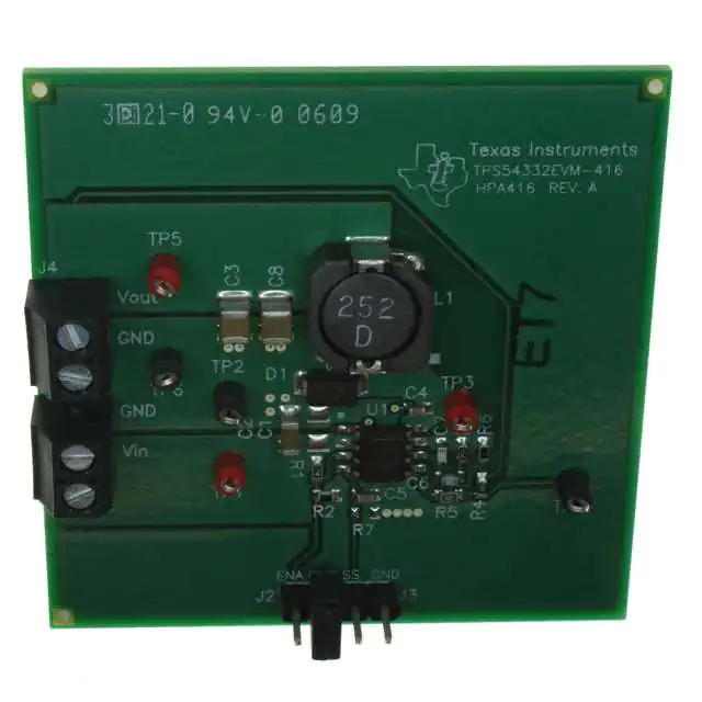
This section provides a description of the TPS54332EVM-416, board layout, and layer illustrations.
3.1 Layout
Figure 3-1 through Figure 3-3 shows the board layout for the TPS54332EVM-416. The top-side layer of the EVM
is laid out in a manner typical of a user application. The top and bottom layers are 2-oz. copper.
The top layer contains the main power traces for VIN, VOUT, and VPHASE. Also on the top layer are connections
for the remaining pins of the TPS54332 and a large area filled with ground. The bottom layer contains ground
and a signal route for the BOOT capacitor. The top and bottom and internal ground traces are connected with
multiple vias placed around the board including ten vias directly under the TPS54332 device to provide a thermal
path from the top-side ground plane to the bottom-side ground plane.
The input decoupling capacitor (C2) and bootstrap capacitor (C4) are all located as close to the IC as possible.
In addition, the voltage set-point resistor divider components are also kept close to the IC. The voltage divider
network ties to the output voltage at the point of regulation, the copper VOUT trace past the output capacitors,
C3 and C8. For the TPS54332, an additional input bulk capacitor can be required, depending on the EVM
connection to the input supply.
Figure 3-1. TPS54332EVM-416 Top-Side Layout
SLVU276A – FEBRUARY 2009 – REVISED OCTOBER 2021
TPS54332 Step-Down Converter Evaluation Module User's Guide
Submit Document Feedback
Copyright © 2022 Texas Instruments Incorporated
11
�Board Layout
www.ti.com
Figure 3-2. TPS54332EVM-416 Bottom-Side Layout
Figure 3-3. TPS54332EVM-416 Top-Side Assembly
3.2 Estimated Circuit Area
The estimated printed circuit board area for the components used in this design is 0.68 in2. This area does not
include test point or connectors.
12
TPS54332 Step-Down Converter Evaluation Module User's Guide
SLVU276A – FEBRUARY 2009 – REVISED OCTOBER 2021
Submit Document Feedback
Copyright © 2022 Texas Instruments Incorporated
�www.ti.com
Schematic and Bill of Materials
4 Schematic and Bill of Materials
This section presents the TPS54332EVM-416 schematic and bill of materials.
4.1 Schematic
Figure 4-1 is the schematic for the TPS54332EVM-416.
Figure 4-1. TPS54332EVM-416 Schematic
SLVU276A – FEBRUARY 2009 – REVISED OCTOBER 2021
TPS54332 Step-Down Converter Evaluation Module User's Guide
Submit Document Feedback
Copyright © 2022 Texas Instruments Incorporated
13
�Schematic and Bill of Materials
www.ti.com
4.2 Bill of Materials
Table 4-1 presents the bill of materials for the TPS54332EVM-416.
Table 4-1. TPS54332EVM-416 Bill of Materials
Count
RefDes
Value
Description
Size
Part Number
MFR
0
C1
Capacitor, Ceramic, 25 V, X5R, 10%
1206
1
C2
10 μF
Capacitor, Ceramic, 25 V, X5R, 10%
1206
GRM31CR61E106KA
12
muRata
1
C3, C8
47 μF
Capacitor, Ceramic, 10 V, X5R, 10%
1210
Std
Std
1
C4
0.1 μF
Capacitor, Ceramic, 16 V, X7R, 10%
0603
Std
Std
1
C5
0.015 μF
Capacitor, Ceramic, 16 V, X7R, 10%
0603
Std
Std
1
C6
180 pF
Capacitor, Ceramic, 50 V, NPO, 5%
0603
Std
Std
1
C7
10 pF
Capacitor, Ceramic, 50 V, NPO, 5%
0603
Std
Std
1
D1
B320A
Diode, Schottky, 3 A, 20 V
SMA 0.27 ×
0.25 inch
B320A
Diodes Inc
2
J1, J4
ED1514
Terminal Block, 2-pin, 6-A, 3.5mm
0.100 × 2
ED1514
OST
2
J2, J3
PTC36SAAN
Header, 2-pin, 100-mil spacing, (36-pin strip) 0.402 × 0.394
inch
PTC36SAAN
1
L1
2.5 μH
Inductor, SMT, 9.26 A, 10 mΩ
0603
MSS1038-252NX_
Coilcraft
1
R1
150 KΩ
Resistor, Chip, 1/16W, 1%
0603
Std
Std
1
R2
48.7 KΩ
Resistor, Chip, 1/16W, 1%
0603
Std
Std
1
R3
75.0 kΩ
Resistor, Chip, 1/16W, 1%
0603
Std
Std
1
R4
0
Resistor, Chip, 1/16W, 1%
0603
Std
Std
1
R5
10.2 kΩ
Resistor, Chip, 1/16W, 1%
0603
Std
Std
1
R6
4.75 kΩ
Resistor, Chip, 1/16W, 1%
0603
Std
Std
0
R7
Resistor, Chip, 1/16W, 1%
0.100 × 0.100
inch
Std
Std
3
TP1,
TP3,
TP5
5000
Test Point, Red, Thru Hole Color Keyed
0.100 × 0.100
inch
5000
Keystone
3
TP2,
TP4,
TP6
5001
Test Point, Black, Thru Hole Color Keyed
SO8[DDA]
5001
Keystone
1
U1
TPS54332DD IC, Step-Down Swift Converter, 3.5 V–28 V,
A
3.5 A
TPS54332DDA
TI
1
PCB
HPA416
Any
1
Shunt
929950-00
3M
5 Revision History
NOTE: Page numbers for previous revisions may differ from page numbers in the current version.
Changes from Revision * (February 2009) to Revision A (October 2021)
Page
• Updated the numbering format for tables, figures, and cross-references throughout the document. ................2
• Updated the user's guide title............................................................................................................................. 2
14
TPS54332 Step-Down Converter Evaluation Module User's Guide
SLVU276A – FEBRUARY 2009 – REVISED OCTOBER 2021
Submit Document Feedback
Copyright © 2022 Texas Instruments Incorporated
�IMPORTANT NOTICE AND DISCLAIMER
TI PROVIDES TECHNICAL AND RELIABILITY DATA (INCLUDING DATA SHEETS), DESIGN RESOURCES (INCLUDING REFERENCE
DESIGNS), APPLICATION OR OTHER DESIGN ADVICE, WEB TOOLS, SAFETY INFORMATION, AND OTHER RESOURCES “AS IS”
AND WITH ALL FAULTS, AND DISCLAIMS ALL WARRANTIES, EXPRESS AND IMPLIED, INCLUDING WITHOUT LIMITATION ANY
IMPLIED WARRANTIES OF MERCHANTABILITY, FITNESS FOR A PARTICULAR PURPOSE OR NON-INFRINGEMENT OF THIRD
PARTY INTELLECTUAL PROPERTY RIGHTS.
These resources are intended for skilled developers designing with TI products. You are solely responsible for (1) selecting the appropriate
TI products for your application, (2) designing, validating and testing your application, and (3) ensuring your application meets applicable
standards, and any other safety, security, regulatory or other requirements.
These resources are subject to change without notice. TI grants you permission to use these resources only for development of an
application that uses the TI products described in the resource. Other reproduction and display of these resources is prohibited. No license
is granted to any other TI intellectual property right or to any third party intellectual property right. TI disclaims responsibility for, and you
will fully indemnify TI and its representatives against, any claims, damages, costs, losses, and liabilities arising out of your use of these
resources.
TI’s products are provided subject to TI’s Terms of Sale or other applicable terms available either on ti.com or provided in conjunction with
such TI products. TI’s provision of these resources does not expand or otherwise alter TI’s applicable warranties or warranty disclaimers for
TI products.
TI objects to and rejects any additional or different terms you may have proposed. IMPORTANT NOTICE
Mailing Address: Texas Instruments, Post Office Box 655303, Dallas, Texas 75265
Copyright © 2022, Texas Instruments Incorporated
�