User's Guide
SLVU972 – September 2013
Evaluation Module for the TPS54340-Q1 Step-Down
Converter
This user's guide contains information for the TPS54340-Q1EVM-593 evaluation module (PWR593)
including the performance specifications, schematic, and the bill of materials.
spacer so the title "List of Tables" will print on page with the list.
1
2
3
4
Contents
Introduction .................................................................................................................. 2
Test Setup and Results .................................................................................................... 5
Board Layout ............................................................................................................... 12
Bill of Materials ............................................................................................................. 15
List of Figures
1
TPS54340-Q1EVM-593 Board ............................................................................................
2
2
TPS54340-Q1EVM-593 Schematic.......................................................................................
3
3
Efficiency versus Load Current............................................................................................
5
4
Light Load Efficiency
.......................................................................................................
Regulation versus Output Current ........................................................................................
Regulation versus Input Voltage ..........................................................................................
Load Transient Response .................................................................................................
Loop Response .............................................................................................................
Line Transient Response ..................................................................................................
Input Voltage Ripple CCM .................................................................................................
Input Voltage Ripple DCM .................................................................................................
Output Voltage Ripple CCM ..............................................................................................
Output Voltage Ripple DCM ..............................................................................................
Output Voltage Ripple Eco-mode .........................................................................................
Switching Waveform Without Snubber ...................................................................................
Switching Waveform With Snubber .......................................................................................
Start Up With VIN Ramping Up ..........................................................................................
Start Up Using EN .........................................................................................................
Prebias Start Up Using EN ...............................................................................................
Shutdown With VIN Ramping Down .....................................................................................
Shutdown Using EN .......................................................................................................
Low Dropout Operation ...................................................................................................
Low Dropout Start Up and Shutdown ...................................................................................
TPS54340-Q1EVM-593 Top Assembly and Silkscreen ..............................................................
TPS54340-Q1EVM-593 Layer 2 Layout ................................................................................
TPS54340-Q1EVM-593 Layer 3 Layout ................................................................................
TPS54340-Q1EVM-593 Bottom-Side Assembly and Silkscreen (Viewed From Top) ............................
5
5
6
7
8
9
10
11
12
13
14
15
16
17
18
19
20
21
22
23
24
25
26
27
6
6
6
6
7
7
7
8
8
8
9
9
10
10
10
11
11
11
11
12
13
13
14
List of Tables
Eco-mode is a trademark of Texas Instruments.
SLVU972 – September 2013
Submit Documentation Feedback
Evaluation Module for the TPS54340-Q1 Step-Down Converter
Copyright © 2013, Texas Instruments Incorporated
1
�Introduction
1
www.ti.com
1
Input Voltage and Output Current Summary ............................................................................
2
TPS54340-Q1EVM-593 Performance Specification Summary .......................................................
3
3
R5 Values for Common Output Voltages ................................................................................
4
4
EVM Connectors and Test points .........................................................................................
5
5
TPS54340-Q1EVM-593 Bill of Materials ...............................................................................
15
2
Introduction
This user's guide contains background information for the TPS54340-Q1 as well as support
documentation for the TPS54340-Q1EVM-593 evaluation module (PWR593). Also included are the
performance specifications, the schematic, and the bill of materials for the TPS54340-Q1EVM-593.
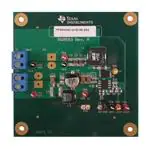
Figure 1. TPS54340-Q1EVM-593 Board
1.1
Background
The TPS54340-Q1 DC-DC converter is designed to provide up to a 3.5-A output from an input voltage
source of 4.5 V to 42 V. Rated input voltage and output current range for the evaluation module are given
in Table 1. This evaluation module is designed to demonstrate the small, printed-circuit-board (PCB) areas
that may be achieved when designing with the TPS54340-Q1 regulator. The switching frequency is
externally set at a nominal 400 kHz. This frequency was chosen to help with Electromagnetic Compatibility
(EMC) by keeping the fundamental frequency out of the typical medium wave (MW) frequency range. The
high-side MOSFET is incorporated inside the TPS54340-Q1 package along with the gate-drive circuitry.
The compensation components are external to the integrated circuit (IC), and an external resistor divider
allows for an adjustable output voltage. Additionally, the TPS54340-Q1 provides an adjustable
undervoltage lockout with hysteresis through an external resistor divider. Lastly, the TPS54340-Q1EVM593 includes additional input filtering and a snubber to reduce emissions. The absolute maximum input
voltage for the TPS54340-Q1EVM-593 is 42 V.
Table 1. Input Voltage and Output Current Summary
1.2
EVM
Input Voltage Range
Output Current Range
TPS54340-Q1EVM-593
VIN = 7.0 V to 42 V
IOUT = 0 A to 3.5 A
Performance Specification Summary
A summary of the TPS54340-Q1EVM-593 (EVM) performance specifications is provided in Table 2.
Specifications are given for an input voltage of VIN = 12 V and an output voltage of 5.0 V, unless otherwise
specified. This EVM is designed and tested for VIN = 7.0 V to 42 V. The ambient temperature is 25°C for
all measurements, unless otherwise noted.
2
Evaluation Module for the TPS54340-Q1 Step-Down Converter
Copyright © 2013, Texas Instruments Incorporated
SLVU972 – September 2013
Submit Documentation Feedback
�Introduction
www.ti.com
Table 2. TPS54340-Q1EVM-593 Performance Specification Summary
Specification
Test Conditions
MIN
TYP
MAX
7
12
42
VIN voltage range
Output voltage set point
Unit
V
5.0
Output current range
VIN = 7 V to 42 V
Line regulation
IOUT = 3.5 A, VIN = 7 V to 42 V
Load regulation
VIN = 12 V, IOUT = 0.001 A to 3.5 A
V
0
IOUT = 0.8 A to 2.6 A
Load transient response
IOUT = 2.6 A to 0.8 A
Loop bandwidth
VIN = 12 V, IOUT = 3.5 A
Phase margin
VIN = 12 V, IOUT = 3.5 A
Input voltage ripple
IOUT = 3.5 A, 20 MHz BWL
Output voltage ripple
IOUT = 3.5 A
3.5
A
±0.02%
±0.2%
Voltage change
250
Recovery time
200
mV
µs
Voltage change
250
mV
Recovery time
300
µs
13
kHz
75
°
很抱歉,暂时无法提供与“TPS54340-Q1EVM-593”相匹配的价格&库存,您可以联系我们找货
免费人工找货- 国内价格 香港价格
- 1+559.740691+70.18655


 工商网监
湘ICP备2023018690号
工商网监
湘ICP备2023018690号