Order
Now
Product
Folder
Support &
Community
Tools &
Software
Technical
Documents
TPS54424
SLVSDV8 – JULY 2017
TPS54424 4.5-V to 17-V (19-V Maximum) Input, 4-A Synchronous
SWIFT™ Step-Down Converter
1 Features
3 Description
•
•
•
The TPS54424 is a full-featured 17-V (19-V
maximum), 4-A synchronous step-down DC/DC
converter in a 3.5 mm × 3.5 mm HotRod™ QFN
package.
Small 3.5-mm × 3.5-mm HotRod™ QFN Package
Integrated 14.1-mΩ and 6.1-mΩ MOSFETs
Peak Current Mode Control With Fast Transient
Response
200-kHz to 1.6-MHz Fixed Switching Frequency
Synchronizes to External Clock
0.6-V Voltage Reference ±0.85% Over
Temperature
0.6-V to 12-V Output Voltage Range
Hiccup Current Limit
Safe Start-Up into Pre-Biased Output Voltage
Adjustable Soft Start and Power Sequencing
Adjustable Input Undervoltage Lockout
3-µA Shutdown Current
Power Good Output Monitor for Undervoltage and
Overvoltage
Output Overvoltage Protection
Non-latch Thermal Shutdown Protection
–40°C to 150°C Operating Junction Temperature
Create a Custom Design Using the TPS54424
With the WEBENCH® Power Designer
1
•
•
•
•
•
•
•
•
•
•
•
•
•
•
2 Applications
•
•
•
•
•
Telecom and Wireless Infrastructure
Test and Measurement
Medical Imaging Equipment
Enterprise Switching
Server
The peak current mode control simplifies the loop
compensation and provides fast transient response.
Cycle-by-cycle peak current limiting on the high-side
and low-side sourcing current limit protects the device
in overload situations. Hiccup limits MOSFET power
dissipation if a short circuit or over loading fault
persists.
A power good supervisor circuit monitors the
regulator output. The PGOOD pin is an open-drain
output and goes high impedance when the output
voltage is in regulation. An internal deglitch time
prevents the PGOOD pin from pulling low unless a
fault has occurred.
A dedicated EN pin can be used to control the
regulator on/off and adjust the input undervoltage
lockout. The output voltage start-up ramp is controlled
by the SS/TRK pin, which allows operation as either a
standalone power supply or in tracking situations.
Device Information(1)
PART NUMBER
TPS54424
VIN
90
CO
FB
RT/CLK
RFBB
COMP
AGND
80
75
70
65
60
PGND
CP
Efficiency (%)
SS/TRK
RT
85
RFBT
PGOOD
RC
95
SW
EN
CSS
100
VOUT
LO
CI
BODY SIZE (NOM)
3.50 mm × 3.50 mm
Efficiency
CBT
BOOT
VIN
PACKAGE
RNV (18)
(1) For all available packages, see the orderable addendum at
the end of the data sheet.
Simplified Schematic
TPS54424
The device is optimized for small solution size
through high efficiency and integrating the high-side
and low-side MOSFETs. Further space savings are
achieved through peak current mode control, which
reduces component count, and by selecting a high
switching frequency, reducing the inductor footprint.
5 V to 1.8 V, 700 kHz, 1.8 µH, 18 m:
9 V to 1.8 V, 700 kHz, 1.8 µH, 18 m:
12 V to 1.8 V, 700 kHz, 1.8 µH, 18 m:
55
CZ
50
0.0
0.5
1.0
1.5
2.0
2.5
Output Current (A)
3.0
3.5
4.0
D001
Copyright © 2017, Texas Instruments Incorporated
1
An IMPORTANT NOTICE at the end of this data sheet addresses availability, warranty, changes, use in safety-critical applications,
intellectual property matters and other important disclaimers. PRODUCTION DATA.
�TPS54424
SLVSDV8 – JULY 2017
www.ti.com
Table of Contents
1
2
3
4
5
6
7
Features ..................................................................
Applications ...........................................................
Description .............................................................
Revision History.....................................................
Pin Configuration and Functions .........................
Specifications.........................................................
1
1
1
2
3
4
6.1
6.2
6.3
6.4
6.5
6.6
6.7
6.8
4
4
5
5
5
7
7
8
Absolute Maximum Ratings ......................................
ESD Ratings..............................................................
Recommended Operating Conditions.......................
Thermal Information ..................................................
Electrical Characteristics...........................................
Switching Characteristics ..........................................
Timing Requirements ................................................
Typical Characteristics ..............................................
7.4 Device Functional Modes........................................ 22
8
Application and Implementation ........................ 23
8.1 Application Information............................................ 23
8.2 Typical Application ................................................. 23
9 Power Supply Recommendations...................... 32
10 Layout................................................................... 32
10.1 Layout Guidelines ................................................. 32
10.2 Layout Example .................................................... 32
10.3 Alternate Layout Example..................................... 34
11 Device and Documentation Support ................. 35
11.1
11.2
11.3
11.4
11.5
11.6
Detailed Description ............................................ 13
7.1 Overview ................................................................. 13
7.2 Functional Block Diagram ....................................... 14
7.3 Feature Description................................................. 14
Document Support ................................................
Receiving Notification of Documentation Updates
Community Resources..........................................
Trademarks ...........................................................
Electrostatic Discharge Caution ............................
Glossary ................................................................
35
35
35
35
35
35
12 Mechanical, Packaging, and Orderable
Information ........................................................... 35
4 Revision History
2
DATE
REVISION
NOTES
July 2017
*
Initial release.
Submit Documentation Feedback
Copyright © 2017, Texas Instruments Incorporated
Product Folder Links: TPS54424
�TPS54424
www.ti.com
SLVSDV8 – JULY 2017
5 Pin Configuration and Functions
RNV Package
18-Pin VQFN-HR
18 PGOOD
17 EN
16 SS/TRK
15 COMP
14 FB
13 RT/CLK
13 RT/CLK
Bottom View
14 FB
15 COMP
16 SS/TRK
17 EN
18 PGOOD
Top View
12 AGND
BOOT 1
1 BOOT
AGND 12
11 VIN
VIN 2
2 VIN
VIN 11
PGND 3
10 PGND
PGND 4
9 PGND
PGND 5
8 PGND
6
SW
PGND 10
3 PGND
PGND 9
4 PGND
PGND 8
5 PGND
7
SW
7
SW
6
SW
Pin Functions
PIN
I/O
DESCRIPTION
NAME
NO.
BOOT
1
I
Floating supply voltage for high-side MOSFET gate drive circuit. Connect a 0.1-µF ceramic
capacitor between BOOT and SW pins.
2, 11
I
Input voltage supply pin. Power for the internal circuit and the connection to drain of highside MOSFET. Connect both pins to the input power source with a low impedance
connection. Connect both pins and their neighboring PGND pins.
3, 4, 5, 8, 9,
10
–
Ground return for low-side power MOSFET and its drivers.
SW
6, 7
O
Switching node. Connected to the source of the high-side MOSFET and drain of the low-side
MOSFET.
AGND
12
–
Ground of internal analog circuitry. AGND must be connected to the PGND plane.
RT/CLK
13
I
Switching frequency setting pin. In RT mode, an external timing resistor adjusts the switching
frequency. In CLK mode, the device synchronizes to an external clock input to this pin.
FB
14
I
Converter feedback input. Connect to the output voltage with a resistor divider.
COMP
15
I
Error amplifier output and input to the PWM modulator. Connect loop compensation to this
pin.
SS/TRK
16
I
Soft-start and tracking pin. Connecting an external capacitor sets the soft-start time. This pin
can also be used for tracking and sequencing.
EN
17
I
Enable pin. Float or pull high to enable the device. Connect a resistor divider to this pin to
implement adjustable under voltage lockout and hysteresis.
PGOOD
18
O
Open-drain power good indicator. It is asserted low if output voltage is outside if the PGOOD
thresholds, VIN is low, EN is low, device is in thermal shutdown or device is in soft-start.
VIN
PGND
Submit Documentation Feedback
Copyright © 2017, Texas Instruments Incorporated
Product Folder Links: TPS54424
3
�TPS54424
SLVSDV8 – JULY 2017
www.ti.com
6 Specifications
6.1 Absolute Maximum Ratings
over operating free-air temperature range (unless otherwise noted) (1)
MIN
Voltage
MAX
VIN
–0.3
19
BOOT
–0.3
27
BOOT (10 ns transient)
–0.3
30
BOOT (vs SW)
–0.3
7
SW
–1
20
SW (10 ns transient)
–3
23
EN, SS/TRK, PGOOD, RT/CLK, FB, COMP
UNIT
V
–0.3
6.5
Operating Junction Temperature Range, TJ
-40
150
°C
Storage Temperature Range, TSTG
-55
150
°C
(1)
Stresses beyond those listed under Absolute Maximum Ratings may cause permanent damage to the device. These are stress ratings
only, which do not imply functional operation of the device at these or any other conditions beyond those indicated under Recommended
Operating Conditions. Exposure to absolute-maximum-rated conditions for extended periods may affect device reliability.
6.2 ESD Ratings
VALUE
V(ESD)
(1)
(2)
4
Electrostatic discharge
Human body model (HBM), per
ANSI/ESDA/JEDEC JS-001, all pins (1)
±2000
Charged device model (CDM), per
JEDEC specification JESD22-C101, all
pins (2)
±500
UNIT
V
JEDEC document JEP155 states that 500-V HBM allows safe manufacturing with a standard ESD control process.
JEDEC document JEP157 states that 250-V CDM allows safe manufacturing with a standard ESD control process.
Submit Documentation Feedback
Copyright © 2017, Texas Instruments Incorporated
Product Folder Links: TPS54424
�TPS54424
www.ti.com
SLVSDV8 – JULY 2017
6.3 Recommended Operating Conditions
over operating free-air temperature range (unless otherwise noted)
Parameter
MIN
NOM
MAX
UNIT
VIN
Input voltage range
4.5
17
V
VOUT
Output Voltage
0.6
12
V
IOUT
Output current
TJ
Operating junction temperature
fSW
Switching Frequency (RT mode and PLL
mode)
4
A
-40
150
°C
200
1600
kHz
6.4 Thermal Information
TPS54424
THERMAL METRIC (1)
RNV
UNIT
18 PINS
ThetaJA
Junction-to-ambient thermal resistance JEDEC
ThetaJA
Junction-to-ambient thermal resistance EVM
57.1
°C/W
34
ThetaJCtop
°C/W
Junction-to-case (top) thermal resistance
26.3
°C/W
ThetaJB
Junction-to-board thermal resistance
18.8
°C/W
PsiJT
Junction-to-top characterization parameter
0.8
°C/W
PsiJB
Junction-to-board characterization parameter
18.8
°C/W
ThetaJCbot
Junction-to-case (bottom) thermal resistance
1.2
°C/W
(1)
For more information about traditional and new thermal metrics, see the Semiconductor and IC Package Thermal Metrics application
report, SPRA953.
6.5 Electrical Characteristics
TJ = -40°C to 150°C, VIN = 4.5 V to 17 V (unless otherwise noted)
PARAMETER
TEST CONDITIONS
MIN
TYP
MAX
4.1
4.3
UNIT
INPUT VOLTAGE
UVLO_rise
UVLO_fall
V(VIN) rising
VIN under-voltage lockout
UVLO_hys
V(VIN) falling
3.7
V
3.9
V
Hysteresis VIN voltage
0.2
580
800
µA
3
11
µA
1.20
1.26
V
Ivin
Operating non-switching supply current
V(EN) = 5 V, V(FB) = 1.5 V
Ivin_sdn
Shutdown supply current
V(EN) = 0 V
V
ENABLE
Ven_rise
Ven_fall
EN threshold
Ven_hys
EN pin threshold voltage hysteresis
Ip
EN pin sourcing current
Iph
EN pin sourcing current
Ih
EN pin hysteresis current
V(EN) rising
V(EN) falling
1.1
1.15
V
50
mV
V(EN) = 1.1V
1.2
µA
V(EN) = 1.3V
4.8
µA
3.6
µA
FB
VFB
Regulated FB voltage
TJ = 25°C
596
600
604
mV
595
600
605
mV
ERROR AMPLIFIER
gmea
Error Amplifier Transconductance (gm)
–2 µA < I(COMP) < 2 µA, V(COMP) = 1 V
Error Amplifier DC gain
1100
µA/V
80
dB
Icomp_src
Error Amplifier source current
V(FB) = 0 V
100
µA
Icomp_snk
Error Amplifier sink current
V(FB) = 2 V
-100
µA
gmps
Power Stage Transconductance
17
A/V
SOFT-START
Iss
Soft-start current
V(SS/TRK) to V(FB) matching
V(SS/TRK) = 0.4 V
5
µA
25
mV
Submit Documentation Feedback
Copyright © 2017, Texas Instruments Incorporated
Product Folder Links: TPS54424
5
�TPS54424
SLVSDV8 – JULY 2017
www.ti.com
Electrical Characteristics (continued)
TJ = -40°C to 150°C, VIN = 4.5 V to 17 V (unless otherwise noted)
PARAMETER
TEST CONDITIONS
MIN
TYP
MAX
UNIT
MOSFET
Rds(on)_h
Rds(on)_l
High-side switch resistance
Low-side switch resistance
TA = 25°C, V(VIN) = 12 V
14.1
mΩ
TA = 25°C, V(VIN) = 4.5 V, V(BOOT-SW) = 4.5 V
15.9
mΩ
TA = 25°C, V(VIN) = 12 V
6.1
mΩ
TA = 25°C, V(VIN) = 4.5 V
6.9
BOOT UVLO Falling
mΩ
2.2
2.6
V
6.8
8.5
A
CURRENT LIMIT
Ioc_HS_pk
High-side peak current limit
V(VIN) = 12 V
Ioc_LS_snk
Low-side sinking current limit
V(VIN) = 12 V
Ioc_LS_src
Low-side sourcing current limit
V(VIN) = 12 V
5.6
-3.4
4.8
6.2
A
7.3
A
RT/CLK
VIH
Logic high input voltage
VIL
Logic low input voltage
2
V
0.8
V
PGOOD
Power good threshold
V(FB) rising (fault)
108
%
V(FB) falling (good)
106
%
V(FB) rising (good)
91
%
V(FB) falling (fault)
89
%
5
nA
Ipg_lkg
Leakage current into PGOOD pin when
pulled high
V(PGOOD) = 5 V
Vpg_low
PGOOD voltage when pulled low
I(PGOOD) = 2 mA
Minimum VIN for valid output
V(PGOOD) < 0.5 V, I(PGOOD) = 4 mA
0.7
Temperature Rising
170
°C
15
°C
0.3
V
1
V
Thermal protection
TTRIP
Thermal protection trip point
THYST
Thermal protection hysteresis
6
Submit Documentation Feedback
Copyright © 2017, Texas Instruments Incorporated
Product Folder Links: TPS54424
�TPS54424
www.ti.com
SLVSDV8 – JULY 2017
6.6 Switching Characteristics
TJ = -40°C to 150°C, V(VIN) = 4.5 V to 17 V (unless otherwise noted)
PARAMETER
TEST CONDITIONS
MIN
TYP
MAX
UNIT
EN
EN to start of switching
135
µs
Deglitch time PGOOD going high
272
Cycles
Deglitch time PGOOD going low
16
Cycles
PGOOD
SW
ton_min
Minimum on time
(1)
toff_min
Minimum off time
(2)
Measured at 50% to 50% of VIN, L = 1.5 µH,
IOUT = 0 A
90
V(BOOT-SW) ≥ 2.6 V
130
ns
0
ns
RT/CLK
fsw_min
Minimum switching frequency (RT mode)
R(RT/CLK) = 250 kΩ
Switching frequency (RT mode)
R(RT/CLK) = 100 kΩ
fsw_max
Maximum switching frequency (RT mode)
R(RT/CLK) = 30.1 kΩ
fsw_clk
Switching frequency synchronization range
(PLL mode)
200
450
500
550
1.6
200
RT/CLK falling edge to SW rising edge
delay (PLL mode)
kHz
Measure at 500kHz with RT resistor in
series with RT/CLK
kHz
MHz
1600
kHz
70
ns
512
Cycles
16384
Cycles
HICCUP
Wait time before hiccup
Hiccup time before restart
(1)
(2)
Characterized. Not production tested.
Specified by design.
6.7 Timing Requirements
TJ = -40°C to 150°C, V(VIN) = 4.5 V to 17 V (unless otherwise noted)
MIN
Minimum synchronization signal pulse width
(PLL mode)
NOM
MAX
35
UNIT
ns
Submit Documentation Feedback
Copyright © 2017, Texas Instruments Incorporated
Product Folder Links: TPS54424
7
�TPS54424
SLVSDV8 – JULY 2017
www.ti.com
100
100
95
95
90
90
85
85
Efficiency (%)
Efficiency (%)
6.8 Typical Characteristics
80
75
70
80
75
70
65
65
60
60
VIN = 9 V
VIN = 12 V
55
VIN = 5 V
VIN = 9 V
VIN = 12 V
55
50
50
0
0.5
1
VOUT = 5 V
WE 744311220
1.5
2
2.5
Output Current (A)
3
3.5
0
4
fSW = 800 kHz
L = 2.2 µH
TA = 25 °C
DCR = 11.4 mΩ
100
95
95
90
90
85
85
Efficiency (%)
Efficiency (%)
1.5
2
2.5
Output Current (A)
3
3.5
4
D003
fSW = 700 kHz
L = 2.2 µH
TA = 25 °C
DCR = 11.4 mΩ
Figure 2. Efficiency for 3.3 V Output
100
80
75
70
65
80
75
70
65
60
60
VIN = 5 V
VIN = 9 V
VIN = 12 V
55
VIN = 5 V
VIN = 9 V
VIN = 12 V
55
50
50
0
0.5
1
VOUT = 2.5 V
WE 744311220
1.5
2
2.5
Output Current (A)
3
3.5
4
0
0.5
1
D004
fSW = 700 kHz
L = 2.2 µH
TA = 25 °C
DCR = 11.4 mΩ
VOUT = 1.5 V
WE 74438357018
Figure 3. Efficiency for 2.5 V Output
1.5
2
2.5
Output Current (A)
3
3.5
4
D006
fSW = 700 kHz
L = 1.8 µH
TA = 25 °C
DCR = 18 mΩ
Figure 4. Efficiency for 1.5 V Output
100
100
95
95
90
90
85
85
Efficiency (%)
Efficiency (%)
1
VOUT = 3.3 V
WE 744311220
Figure 1. Efficiency for 5 V Output
80
75
70
65
80
75
70
65
60
60
VIN = 5 V
VIN = 9 V
VIN = 12 V
55
VIN = 5 V, fSW = 600 kHz
VIN = 9 V, fSW = 600 kHz
VIN = 12 V, fSW = 500 kHz
55
50
50
0
0.5
VOUT = 1.2 V
WE 74438357012
1
1.5
2
2.5
Output Current (A)
fSW = 600 kHz
L = 1.2 µH
3
3.5
4
0
0.5
D007
TA = 25 °C
DCR = 13.4 mΩ
VOUT = 1.0 V
WE 74438357012
Figure 5. Efficiency for 1.2 V Output
8
0.5
D002
Submit Documentation Feedback
1
1.5
2
2.5
Output Current (A)
TA = 25 °C
L = 1.2 µH
3
3.5
4
D008
TA = 25 °C
DCR = 13.4 mΩ
Figure 6. Efficiency for 1.0 V Output
Copyright © 2017, Texas Instruments Incorporated
Product Folder Links: TPS54424
�TPS54424
www.ti.com
SLVSDV8 – JULY 2017
Typical Characteristics (continued)
10
VIN = 4.5 V
VIN = 12 V
VIN = 17 V
610
600
VIN Pin Shutdown Supply Current (PA)
Nonswitching Supply Current (PA)
620
590
580
570
560
550
540
530
520
510
500
-50
-25
0
V(EN) = 5 V
25
50
75
100
Junction Temperature (qC)
125
VIN = 4.5 V
VIN = 12 V
VIN = 17 V
9
8
7
6
5
4
3
2
1
0
-50
150
V(FB) = 0.8 V
5.5
1.2
EN Pin Output Current (PA)
EN Voltage Threshold (V)
6
1.21
1.19
1.18
1.17
1.16
1.15
1.14
EN Rising
EN Falling
-25
0
25
50
75
100
Junction Temperature (qC)
125
4
3.5
V(EN) = 1.1 V
V(EN) = 1.3 V
3
2.5
2
1.5
1
MOSFET Rds(on) (m:)
0.602
0.601
0.6
0.599
0.598
0.597
0.596
25
50
75
100
Junction Temperature (qC)
-25
0
125
25
50
75
100
Junction Temperature (qC)
125
150
D008
D007
Figure 10. EN Pin Current vs Junction Temperature
0.603
Voltage Reference (V)
D006
5
D007
0.604
0
150
4.5
0
-50
150
0.605
-25
125
0.5
Figure 9. EN Pin Voltage Threshold vs Junction
Temperature
0.595
-50
25
50
75
100
Junction Temperature (qC)
Figure 8. VIN Pin Shutdown Current vs Junction
Temperature
1.22
1.12
-50
0
V(EN) = 0.4 V
Figure 7. VIN Pin Nonswitching Supply Current vs Junction
Temperature
1.13
-25
D005
150
28
26
24
22
20
18
16
14
12
10
8
6
4
2
-50
High-side, V(BOOT-SW) = 4.5 V
High-side, V(VIN) = 12 V
Low-side, V(VIN) = 4.5 V
Low-side, V(VIN) = 12 V
-25
D009
Figure 11. Regulated FB Voltage vs Junction Temperature
0
25
50
75
100
Junction Temperature (qC)
125
150
D010
Figure 12. MOSFET Rds(on) vs Junction Temperature
Submit Documentation Feedback
Copyright © 2017, Texas Instruments Incorporated
Product Folder Links: TPS54424
9
�TPS54424
SLVSDV8 – JULY 2017
www.ti.com
Typical Characteristics (continued)
19
V(COMP) to I(SW) Transconductance (S)
Error Amplifier Transconductance (PS)
1400
1350
1300
1250
1200
1150
1100
1050
1000
950
900
-50
-25
0
25
50
75
100
Junction Temperature (qC)
125
17
16
15
14
13
12
-50
150
-25
0
D011
Figure 13. Error Amplifier Transconductance vs Junction
Temperature
40
38
V(SS/TRK) to V(FB) matching (mV)
5.3
5.15
5.1
5.05
5
4.95
4.9
4.85
4.8
25
50
75
100
Ambient Temperature (qC)
125
150
D009
Figure 14. COMP to SW Transconductance vs Junction
Temperature
5.25
5.2
I(SS/TRK) (µA)
18
36
34
32
30
28
26
24
22
4.75
4.7
-50
-25
0
25
50
75
100
Junction Temperature (qC)
125
20
-50
150
-25
0
D013
25
50
75
100
Junction Temperature (qC)
125
150
D014
V(SS/TRK) = 0.4 V
8
0.7
0.65
0.6
0.55
0.5
0.45
0.4
0.35
0.3
0.25
0.2
0.15
0.1
0.05
0
0
0.2
0.4
0.6
0.8
1
V(SS/TRK) (V)
1.2
1.4
1.6
1.8
VIN = 4.5 V
VIN = 12 V
VIN = 17 V
7.75
7.5
7.25
7
6.75
6.5
6.25
6
-50
D022
Figure 17. FB voltage vs SS/TRK Voltage
10
Figure 16. SS/TRK to FB Offset vs Junction Temperature
High-side Peak Current Limit (A)
V(FB) (V)
Figure 15. SS/TRK Current vs Junction Temperature
-25
0
25
50
75
100
Junction Temperature (qC)
125
150
D010
Figure 18. High-side Peak Current Limit vs Junction
Temperature
Submit Documentation Feedback
Copyright © 2017, Texas Instruments Incorporated
Product Folder Links: TPS54424
�TPS54424
www.ti.com
SLVSDV8 – JULY 2017
Typical Characteristics (continued)
106
100
PGOOD Leakage Current (nA)
1000
of VREF)
1100
108
PGOOD Threshold (
110
104
102
V(FB) falling (fault)
V(FB) rising (good)
V(FB) rising (fault)
V(FB) falling (good)
98
96
94
92
90
900
800
700
600
500
400
300
200
100
88
86
-50
-25
0
25
50
75
100
Junction Temperature (qC)
125
0
-50
150
-25
0
D016
25
50
75
100
Junction Temperature (qC)
V(FB) = 0.6 V
Figure 19. PGOOD Thresholds vs Junction Temperature
520
105
515
Switching Frequency (kHz)
Minimum on-time (ns)
95
90
85
80
75
70
IOUT = 0 A
IOUT = 0.1 A
IOUT = 0.5 A
65
60
-50
-25
0
VIN = 12 V
25
50
75
100
Ambient Temperature (qC)
125
D017
V(PGOOD) = 5 V
510
505
500
495
490
485
480
-50
150
-25
0
D011
25
50
75
100
Junction Temperature (qC)
125
150
D020
R(RT/CLK) = 100 kΩ
L = 1.5 µH
Figure 22. Switching Frequency vs Junction Temperature
(500 kHz)
Figure 21. Minimum on-time vs Ambient Temperature
650
1660
1650
600
1640
Switching Frequency (kHz)
Switching Frequency (kHz)
150
Figure 20. PGOOD Leakage Current vs Junction
Temperature
110
100
125
1630
1620
1610
1600
1590
1580
1570
550
500
450
400
350
300
1560
250
1550
1540
-50
-25
0
25
50
75
100
Junction Temperature (qC)
125
150
200
80
100
D021
120
140
160 180 200
R(RT/CLK) (k:)
220
240
260
D023
R(RT/CLK) = 30.1 kΩ
Figure 23. Switching Frequency vs Junction Temperature
(1600 kHz)
Figure 24. Switching Frequency vs RT/CLK Resistor (Low
Range)
Submit Documentation Feedback
Copyright © 2017, Texas Instruments Incorporated
Product Folder Links: TPS54424
11
�TPS54424
SLVSDV8 – JULY 2017
www.ti.com
Typical Characteristics (continued)
1600
Switching Frequency (kHz)
1500
1400
1300
1200
1100
1000
900
800
700
600
25
30
35
40
45
50 55 60 65
R(RT/CLK) (k:)
70
75
80
85
D024
Figure 25. Switching Frequency vs RT/CLK Resistor (High Range)
12
Submit Documentation Feedback
Copyright © 2017, Texas Instruments Incorporated
Product Folder Links: TPS54424
�TPS54424
www.ti.com
SLVSDV8 – JULY 2017
7 Detailed Description
7.1 Overview
The TPS54424 is a 17-V, 4-A, synchronous step-down (buck) converter with two integrated n-channel
MOSFETs. To improve performance during line and load transients the device implements a constant frequency,
peak current mode control which also simplifies external frequency compensation. The wide switching frequency
of 200 kHz to 1600 kHz allows for efficiency and size optimization when selecting the output filter components.
The switching frequency is adjusted using a resistor to ground on the RT/CLK pin. The TPS54424 also has an
internal phase lock loop (PLL) connected to the RT/CLK pin that can be used to synchronize the switching cycle
to the falling edge of an external system clock.
The integrated MOSFETs allow for high efficiency power supply designs with continuous output currents up to 4
amperes. The MOSFETs have been sized to optimize efficiency for lower duty cycle applications. The device
reduces the external component count by integrating a bootstrap recharge circuit. The bias voltage for the
integrated high-side MOSFET is supplied by a capacitor between the BOOT and SW pins. The BOOT capacitor
voltage is monitored by a BOOT to SW UVLO (BOOT-SW UVLO) circuit allowing SW pin to be pulled low to
recharge the BOOT capacitor. The device can operate at 100% duty cycle as long as the BOOT capacitor
voltage is higher than the preset BOOT-SW UVLO threshold which is typically 2.2 V.
The TPS54424 has been designed for safe monotonic startup into pre-biased loads. The default start up is when
VIN is typically 4.1 V. The EN pin has an internal pull-up current source that can be used to adjust the input
voltage under voltage lockout (UVLO) with two external resistors. In addition, the internal pull-up current of the
EN pin allows the device to operate with the EN pin floating. The operating current for the TPS54424 is typically
580 μA when not switching and under no load. When the device is disabled, the supply current is typically 3 μA.
The SS/TRK (soft start/tracking) pin is used to minimize inrush currents or provide power supply sequencing
during power up. A small value capacitor or resistor divider should be coupled to the pin for soft start or critical
power supply sequencing requirements. The output voltage can be stepped down to as low as the 0.6 V voltage
reference (VREF). The device has a power good comparator (PGOOD) with hysteresis which monitors the output
voltage through the FB pin. The PGOOD pin is an open drain MOSFET which is pulled low when the FB pin
voltage is less than 89% or greater than 108% of the reference voltage VREF and asserts high when the FB pin
voltage is 91% to 106% of VREF.
The device is protected from output overvoltage, overload and thermal fault conditions. The device minimizes
excessive output overvoltage transients by taking advantage of the overvoltage circuit power good comparator.
When the overvoltage comparator is activated, the high-side MOSFET is turned off and prevented from turning
on until the FB pin voltage is lower than 106% of the VREF. The device implements both high-side MOSFET over
current protection and bidirectional low-side MOSFET over current protections which help control the inductor
current and avoid current runaway. The device also shuts down if the junction temperature is higher than thermal
shutdown trip point. The device is restarted under control of the soft start circuit automatically when the junction
temperature drops 15°C typically below the thermal shutdown trip point.
Submit Documentation Feedback
Copyright © 2017, Texas Instruments Incorporated
Product Folder Links: TPS54424
13
�TPS54424
SLVSDV8 – JULY 2017
www.ti.com
7.2 Functional Block Diagram
PGOOD
VIN
EN
Shutdown
Ip
UV
Ih
Enable
Comparator
Thermal
Shutdown
UVLO
Shutdown
Shutdown
Logic
Logic
Enable
Threshold
Hiccup
Shutdown
OV
ERROR
AMPLIFIER
BOOT
Charge
Minimum
Clamp
Pulse Skip
Current
Sense
FB
BOOT
Boot
UVLO
SS/TRK
HS MOSFET
Current
Comparator
Voltage
Reference
Power Stage
& Deadtime
Control
Logic
SW
Slope
Compensation
VIN
Hiccup
Shutdown
Overload
Recovery
Oscillator
with PLL
Maximum
Clamp
LS
MOSFET
Current
Limit
Regulator
Current
Sense
PGND
COMP
RT/CLK
AGND
Copyright © 2016, Texas Instruments Incorporated
7.3 Feature Description
7.3.1 Fixed Frequency PWM Control
The device uses an adjustable fixed frequency, peak current mode control. The output voltage is compared
through external resistors on the FB pin to an internal voltage reference by an error amplifier which drives the
COMP pin. An internal oscillator initiates the turn on of the high-side power switch. The error amplifier output is
converted into a current reference which compares to the high-side power switch current. When the power switch
current reaches current reference generated by the COMP voltage level the high-side power switch is turned off
and the low-side power switch is turned on.
The device adds an internal slope compensation ramp to prevent subharmonic oscillations. The peak inductor
current limit remains constant over the full duty cycle range.
7.3.2 Continuous Conduction Mode Operation (CCM)
As a synchronous buck converter, the device works in CCM (Continuous Conduction Mode) under all load
conditions.
14
Submit Documentation Feedback
Copyright © 2017, Texas Instruments Incorporated
Product Folder Links: TPS54424
�TPS54424
www.ti.com
SLVSDV8 – JULY 2017
Feature Description (continued)
7.3.3 VIN Pins and VIN UVLO
The VIN pin voltage supplies the internal control circuits of the device and provides the input voltage to the power
converter system. The input voltage for VIN can range from 4.5 V to 17 V. The device implements internal UVLO
circuitry on the VIN pin. The device is disabled when the VIN pin voltage falls below the internal VIN UVLO
threshold. The internal VIN UVLO threshold has a hysteresis of 200 mV. A voltage divider connected to the EN
pin can adjust the input voltage UVLO appropriately. See Enable and Adjustable UVLO for more details.
7.3.4 Voltage Reference and Adjusting the Output Voltage
The voltage reference system produces a precise ±0.85%, 0.6 V voltage reference over temperature by scaling
the output of a temperature stable band gap circuit. The output voltage is set with a resistor divider from the
output (VOUT) to the FB pin shown in Figure 26. It is recommended to use 1% tolerance or better divider
resistors. Start with a fixed value for the bottom resistor in the divider, typically 10 kΩ, then use Equation 1 to
calculate the top resistor in the divider. To improve efficiency at light loads consider using larger value resistors.
If the values are too high the regulator is more susceptible to noise and voltage errors from the FB input current
are noticeable. The minimum output voltage and maximum output voltage can be limited by the minimum on time
of the high side MOSFET and bootstrap voltage (BOOT-SW voltage) respectively.
VOUT
TPS54424
RFBT
FB
RFBB
0.6 V
+
Copyright © 2017, Texas Instruments Incorporated
Figure 26. FB Resistor Divider
RFBT
§V
RFBB u ¨ OUT
© VREF
·
1¸
¹
(1)
7.3.5 Error Amplifier
The device uses a transconductance error amplifier. The error amplifier compares the FB pin voltage to the lower
of the SS/TRK pin voltage or the internal 0.6-V voltage reference. The transconductance of the error amplifier is
1100 μA/V. The frequency compensation network is connected between the COMP pin and ground.
When operating at current limit the COMP pin voltage is clamped to a maximum level to improve response when
the load current decreases. When FB is greater than the internal voltage reference or SS/TRK the COMP pin
voltage is clamped to a minimum level and the devices enters a high-side skip mode.
7.3.6 Enable and Adjustable UVLO
The EN pin provides on/off control of the device. Once the EN pin voltage exceeds its threshold voltage, the
device starts operation. If the EN pin voltage is pulled below the threshold voltage, the regulator stops switching
and enters low operating current state. The EN pin has an internal pull-up current source, Ip, allowing the user to
float the EN pin for enabling the device. If an application requires controlling the EN pin, an open drain or open
collector output logic can be interfaced with the pin.
Submit Documentation Feedback
Copyright © 2017, Texas Instruments Incorporated
Product Folder Links: TPS54424
15
�TPS54424
SLVSDV8 – JULY 2017
www.ti.com
Feature Description (continued)
An external resistor divider can be added from VIN to the EN pin for adjustable UVLO and hysteresis as shown
in Figure 27. The EN pin has a small pull-up current Ip which sets the default state of the pin to enable when no
external components are connected. The pull-up current is also used to control the voltage hysteresis for the
UVLO function since it increases by Ih once the EN pin crosses the enable threshold. The UVLO thresholds can
be calculated using Equation 2 and Equation 3. When using the adjustable UVLO function, 500 mV or greater
hysteresis is recommended. For applications with very slow input voltage slew rate, a capacitor can be placed
from the EN pin to ground to filter any glitches on the input voltage.
TPS54424
VIN
Ip
Ih
RENT
EN
+
RENB
Copyright © 2017, Texas Instruments Incorporated
Figure 27. Adjustable UVLO Using EN
RENT
§V
·
VSTART u ¨ ENFALLING ¸ VSTOP
© VENRISING ¹
§
·
V
Ip u ¨ 1 ENFALLING ¸ Ih
VENRISING ¹
©
(2)
vertical spacer
RENB
RENT u VENFALLING
VSTOP
VENFALLING
RENT u Ip
Ih
(3)
7.3.7 Soft Start and Tracking
The TPS54424 regulates to the SS/TRK pin while its voltage is lower than the internal reference to implement
soft start. A capacitor on the SS/TRK pin to ground sets the soft start time. The SS/TRK pin has an internal pullup current source of 5 μA that charges the external soft start capacitor. Equation 4 calculates the required soft
start capacitor value. The FB voltage will follow the SS/TRK pin voltage with a 25 mV offset up to 90% of the
internal voltage reference. When the SS/TRK voltage is greater than 90% of the internal reference voltage the
offset increases as the effective system reference transitions from the SS/TRK voltage to the internal voltage
reference.
CSS nF
ISS µA u tSS ms
VREF V
8.3 u t SS ms
(4)
If during normal operation, VIN goes below the UVLO, EN pin pulled below 1.15 V, or a thermal shutdown event
occurs, the TPS54424 stops switching and the SS/TRK pin floats. When the VIN goes above UVLO, EN goes
above 1.20 V, or a thermal shutdown is exited, the SS/TRK pin is discharged to near ground before reinitiating a
powering up sequence.
16
Submit Documentation Feedback
Copyright © 2017, Texas Instruments Incorporated
Product Folder Links: TPS54424
�TPS54424
www.ti.com
SLVSDV8 – JULY 2017
Feature Description (continued)
When the COMP pin voltage is clamped by the maximum COMP clamp in an overload condition the SS/TRK pin
is discharged to near the FB voltage. When the overload condition is removed, the soft-start circuit controls the
recovery from the fault output level to the nominal output regulation voltage. At the beginning of recovery a spike
in the output voltage may occur while the COMP voltage transitions from the maximum clamp to the value
determined by the loop.
7.3.8 Safe Start-up into Pre-Biased Outputs
The device has been designed to prevent the low-side MOSFET from discharging a pre-biased output. During
monotonic pre-biased startup, the low-side MOSFET is not allowed to sink current until the SS/TRK pin voltage is
higher than the FB pin voltage and the high-side MOSFET begins to switch. The one exception is if the BOOTSW voltage is below the UVLO threshold. While in BOOT-SW UVLO, the low-side MOSFET is allowed to turn on
to charge the BOOT capacitor. The low-side MOSFET reverse current protection provides another layer of
protection for the device after the high-side MOSFET begins to switch.
7.3.9 Power Good
The PGOOD pin is an open-drain output requiring an external pull-up resistor to output a high signal. Once the
FB pin is between 91% and 106% of the internal voltage reference and SS/TRK is greater than 0.75 V, after a
272 cycle deglitch time the PGOOD pin is de-asserted and the pin floats. A pull-up resistor between the values of
10 kΩ and 100 kΩ to a voltage source that is 6.5 V or less is recommended. PGOOD is in a defined state once
the VIN input voltage is greater than 1 V but with reduced current sinking capability.
When the FB is lower than 89% or greater than 108% of the nominal internal reference voltage, after a 16 cycle
deglitch time the PGOOD pin is pulled low. PGOOD is immediately pulled low if VIN falls below its UVLO, EN pin
is pulled low or the TPS54424 enters thermal shutdown.
Submit Documentation Feedback
Copyright © 2017, Texas Instruments Incorporated
Product Folder Links: TPS54424
17
�TPS54424
SLVSDV8 – JULY 2017
www.ti.com
Feature Description (continued)
7.3.10 Sequencing (SS/TRK)
Many of the common power supply sequencing methods can be implemented using the SS/TRK, EN and
PGOOD pins.
The sequential method is illustrated in Figure 28 using two TPS54424 or similar devices. The power good of the
first device is coupled to the EN pin of the second device which enables the second power supply once the
primary supply reaches regulation.
Figure 29 shows the method implementing ratiometric sequencing by connecting the SS/TRK pins of two devices
together. The regulator outputs ramp up and reach regulation at the same time. When calculating the soft-start
time the current source must be doubled in Equation 4.
TPS54424
TPS54424
TPS54424
PGOOD
EN
EN
SS/TRK
SS/TRK
EN
PGOOD
SS/TRK
PGOOD
Copyright © 2017, Texas Instruments Incorporated
TPS54424
EN
SS/TRK
PGOOD
Copyright © 2017, Texas Instruments Incorporated
Figure 28. Sequential Start-Up Sequence
18
Figure 29. Ratiometric Start-Up Sequence
Submit Documentation Feedback
Copyright © 2017, Texas Instruments Incorporated
Product Folder Links: TPS54424
�TPS54424
www.ti.com
SLVSDV8 – JULY 2017
Feature Description (continued)
Ratiometric and simultaneous power supply sequencing can be implemented by connecting the resistor network
of RTRT and RTRB shown in Figure 30 to the output of the power supply that needs to be tracked or another
voltage reference source. Using Equation 6 and Equation 7, the tracking resistors can be calculated to initiate the
VOUT2 slightly before, after or at the same time as VOUT1. Equation 5 is the voltage difference between VOUT1 and
VOUT2.
To design a ratiometric start-up in which the VOUT2 voltage is slightly greater than the VOUT1 voltage when VOUT2
reaches regulation, use a negative number in Equation 6 and Equation 7 for deltaV. Equation 5 results in a
positive number for applications where the VOUT2 is slightly lower than VOUT1 when VOUT2 regulation is achieved.
The deltaV variable is zero volts for simultaneous sequencing. To minimize the effect of the inherent SS/TRK to
FB offset (Vssoffset = 25 mV) in the soft-start circuit and the offset created by the pull-up current source (Iss = 5
μA) and tracking resistors, the Vssoffset and Iss are included as variables in the equations.
To ensure proper operation of the device, the calculated RTRT value from Equation 6 must be greater than the
value calculated in Equation 8.
'V
VOUT1 VOUT2
(5)
vertical spacer
RTRT
VOUT2 'V Vssoffset
u
VREF
Iss
(6)
vertical spacer
RTRB
VREF u RTRT
VOUT2 'V VREF
(7)
vertical spacer
RTRT ! 2800 u VOUT1 180 u 'V
(8)
TPS54424
VOUT1
EN
SS/TRK
PGOOD
TPS54424
VOUT2
EN
RTRT
SS/TRK
RTRB
RFBT
PGOOD
RFBB
Copyright © 2017, Texas Instruments Incorporated
Figure 30. Ratiometric and Simultaneous Start-Up Sequence
Submit Documentation Feedback
Copyright © 2017, Texas Instruments Incorporated
Product Folder Links: TPS54424
19
�TPS54424
SLVSDV8 – JULY 2017
www.ti.com
Feature Description (continued)
7.3.11 Adjustable Switching Frequency (RT Mode)
In RT mode, a resistor (RT resistor) is connected between the RT/CLK pin and AGND. The switching frequency
of the device is adjustable from 200 kHz to 1600 kHz by placing a maximum of 250 kΩ and minimum of 30.1 kΩ
respectively. To determine the RT resistance for a given switching frequency, use Equation 9. To reduce the
solution size one would set the switching frequency as high as possible, but tradeoffs of the supply efficiency and
minimum controllable on-time should be considered. Equation 10 can be used to calculate the switching
frequency for a given RT resistance.
RT k:
58650 u fSW kHz
1.028
(9)
vertical spacer
fSW kHz
43660 u RT k:
0.973
(10)
7.3.12 Synchronization (CLK Mode)
An internal Phase Locked Loop (PLL) has been implemented to allow synchronization from 200 kHz to 1600 kHz,
and to easily switch from RT mode to CLK mode. To implement the synchronization feature, connect a square
wave clock signal to the RT/CLK pin with a duty cycle from 20% to 80%. If the clock signals rising edge occurs
near the falling edge of SW, increased SW jitter may occur. Use Equation 11 to calculate the maximum clock
pulse width to minimize jitter in CLK mode. The clock signal amplitude must transition lower than 0.8 V and
higher than 2 V. The start of the switching cycle is synchronized to the falling edge of the RT/CLK pin.
æ
ö
V
0.75 ´ ç 1 - OUT ÷
ç
VIN(min ) ÷
è
ø
CLK _ PWMAX =
fSW
(11)
In applications where both RT mode and CLK mode are needed, the device can be configured as shown in
Figure 31. Before the external clock is present, the device works in RT mode and the switching frequency is set
by RT resistor. When the external clock is present, the CLK mode overrides the RT mode. The first time the
SYNC pin is pulled above the RT/CLK high threshold (2 V), the device switches from the RT mode to the CLK
mode and the RT/CLK pin becomes high impedance as the PLL starts to lock onto the frequency of the external
clock.
If the input clock goes away the internal clock frequency begins to drop and after 10 µs without a clock the
device returns to RT mode. Output undershoot while the switching frequency drops can occur. Output overshoot
can also occur when the switching frequency steps back up to the RT mode frequency. A high impedance tristate buffer as shown in Figure 33 is recommended for best performance during the transition from CLK mode to
RT mode because it minimizes the loading on the RT/CLK pin allowing faster transition back to RT mode.
Figure 34 shows the typical performance for the transition from RT mode to CLK mode then back to RT mode.
A series RC circuit as shown in Figure 32 can also be used to interface the RT/CLK pin but the capacitive load
slows down the transition back to RT mode. The series RC circuit is not recommended if the transition from CLK
mode to RT mode is important. A capacitor in the range of 47 pF to 470 pF is recommended. When using the
series RC circuit verify the amplitude of the signal at the RT/CLK pin goes above the high threshold.
20
Submit Documentation Feedback
Copyright © 2017, Texas Instruments Incorporated
Product Folder Links: TPS54424
�TPS54424
www.ti.com
SLVSDV8 – JULY 2017
Feature Description (continued)
RT/CLK Mode Select
TPS54424
TPS54424
RT/CLK
2k
RT/CLK
47 pF
RT
RT
Copyright © 2017, Texas Instruments Incorporated
Copyright © 2017, Texas Instruments Incorporated
Figure 31. Simplified Circuit When Using Both RT
Mode and CLK Mode
TPS54424
OE
Figure 32. Interfacing to the RT/CLK Pin with
Series RC
CH2: VOUT DC OFFSET
RT/CLK
RT
CH3: RT/CLK
CH1: SW
Copyright © 2017, Texas Instruments Incorporated
VIN = 12 V, IOUT = 4 A,
VOUT = 3.3 V, fsw = 1.2 MHz
Figure 33. Interfacing to the RT/CLK Pin with
Buffer
Figure 34. RT to CLK to RT Transition with Buffer
7.3.13 Bootstrap Voltage and 100% Duty Cycle Operation (BOOT)
The device provides an integrated bootstrap voltage regulator. A small capacitor between the BOOT and SW
pins provides the gate drive voltage for the high side MOSFET. The BOOT capacitor is refreshed when the lowside MOSFET is on. The recommended value of the BOOT capacitor is 0.1 μF. A ceramic capacitor with an X7R
or X5R grade dielectric with a voltage rating of 10 V or higher is recommended for stable performance over
temperature and voltage.
When operating with a low voltage difference from input to output, the high side MOSFET of the device will
operate at 100% duty cycle as long as the BOOT to SW pin voltage is greater than 2.2 V. The device will begin
to transition to 100% duty cycle operation when the high-side MOSFET off-time is less than 200 ns typical. When
the voltage from BOOT to SW drops below 2.2 V, the high-side MOSFET is turned off due to BOOT UVLO and
the low side MOSFET pulls SW low to recharge the BOOT capacitor. When operating at 100% duty cycle the
high-side MOSFET can remain on for many switching cycles before the MOSFET is turned off to refresh the
capacitor because the gate drive current sourced by the BOOT capacitor is small. The effective switching
frequency reduced and the effective maximum duty cycle of the switching regulator is near 100%. The output
voltage of the converter during dropout is mainly influenced by the voltage drops across the power MOSFET, the
inductor resistance, and the printed circuit board resistance.
Submit Documentation Feedback
Copyright © 2017, Texas Instruments Incorporated
Product Folder Links: TPS54424
21
�TPS54424
SLVSDV8 – JULY 2017
www.ti.com
Feature Description (continued)
7.3.14 Output Overvoltage Protection (OVP)
The TPS54424 incorporates an output overvoltage protection (OVP) circuit to minimize output voltage overshoot.
The OVP feature minimizes the overshoot by comparing the FB pin voltage to the OVP threshold. The OVP
threshold is the same as the 108% PGOOD threshold. If the FB pin voltage is greater than the OVP threshold
the high-side MOSFET is turned off preventing current from flowing to the output and minimizing output
overshoot. When the high-side MOSFET turns off, the low-side MOSFET turns on and the current in the inductor
discharges. The output voltage can overshoot the OVP threshold as the current in the inductor discharges to 0 A.
When the FB voltage drops lower than the 106% PGOOD threshold, the high-side MOSFET is allowed to turn on
at the next clock cycle.
7.3.15 Overcurrent Protection
The device is protected from overcurrent conditions by cycle-by-cycle current limiting on both the high-side
MOSFET and the low-side MOSFET. In an extended overcurrent condition the device will enter hiccup to reduce
power dissipation.
7.3.15.1 High-side MOSFET Overcurrent Protection
The device implements current mode control which uses the COMP pin voltage to control the turnoff of the highside MOSFET and the turnon of the low-side MOSFET on a cycle-by-cycle basis. Each cycle the switch current
and the current reference generated by the COMP pin voltage are compared, when the peak switch current
intersects the current reference the high-side switch is turned off. The maximum peak switch current through the
high-side MOSFET for overcurrent protection is done by limiting the current reference internally. If the peak
current required to regulate the output is greater than the internal limit, the output voltage is pulled low and the
error amplifier responds by driving the COMP pin high. The maximum COMP voltage is then clamped by an
internal COMP clamp circuit. If the COMP voltage is clamped high for more than the hiccup wait time of 512
switching cycles, the device will shut down itself and restart after the hiccup time of 16384 cycles.
7.3.15.2 Low-side MOSFET Overcurrent Protection
While the low-side MOSFET is turned on the current through it is monitored. During normal operation the lowside MOSFET sources current to the load. At the end of every clock cycle, the low-side MOSFET sourcing
current is compared to the internally set low-side sourcing current limit. If the low-side sourcing current is
exceeded the high-side MOSFET is not turned on and the low-side MOSFET stays on for the next cycle. The
high-side MOSFET is turned on again when the low-side current is below the low-side sourcing current limit at
the start of a cycle. The low-side sourcing current limit prevents current runaway.
The low-side MOSFET may also sink current from the load. If the low-side sinking current limit is exceeded the
low-side MOSFET is turned off immediately for the rest of that clock cycle. In this scenario both MOSFETs are
off until the start of the next cycle. If the low-side MOSFET turns off due to sinking current limit protection, the
low-side MOSFET can only turn on again after the high-side MOSFET turns on then off or if the device enters
BOOT UVLO.
7.4 Device Functional Modes
The EN pin and a VIN UVLO is used to control turn on and turn off of the TPS54424. The device becomes active
when V(VIN) exceeds the 4.1 V typical UVLO and when V(EN) exceeds 1.20 V typical. The EN pin has an internal
current source to enable the output when the EN pin is left floating. If the EN pin is pulled low the device is put
into a low quiescent current state.
22
Submit Documentation Feedback
Copyright © 2017, Texas Instruments Incorporated
Product Folder Links: TPS54424
�TPS54424
www.ti.com
SLVSDV8 – JULY 2017
8 Application and Implementation
NOTE
Information in the following applications sections is not part of the TI component
specification, and TI does not warrant its accuracy or completeness. TI’s customers are
responsible for determining suitability of components for their purposes. Customers should
validate and test their design implementation to confirm system functionality.
8.1 Application Information
The TPS54424 is a synchronous buck converter designed for 4.5 V to 17 V input and 4-A load. This procedure
illustrates the design of a high-frequency switching regulator using ceramic output capacitors. Alternatively the
WEBENCH® software can be used to generate a complete design. The WEBENCH® software uses an interactive
design procedure and accesses a comprehensive database of components when generating a design. This
section presents a simplified discussion of the design process.
8.2 Typical Application
Figure 35. TPS54424 4.5-V to 15-V Input, 1.8-V Output Converter Application Schematic
8.2.1 Design Requirements
For this design example, use the parameters shown in Table 1.
Table 1. Design Parameters
PARAMETER
EXAMPLE VALUE
Input voltage range (VIN)
4.5 to 15 V, 12 V Nominal
Output voltage (VOUT)
1.8 V
Transient response
+/- 4%, +/- 72 mV
Output ripple voltage
0.5%, 9 mV
Output current rating (IOUT)
4A
Operating frequency (fSW)
700 kHz
8.2.2 Detailed Design Procedure
8.2.2.1 Custom Design With WEBENCH® Tools
Click here to create a custom design using the TPS54424 device with the WEBENCH® Power Designer.
1. Start by entering the input voltage (VIN), output voltage (VOUT), and output current (IOUT) requirements.
2. Optimize the design for key parameters such as efficiency, footprint, and cost using the optimizer dial.
3. Compare the generated design with other possible solutions from Texas Instruments.
Submit Documentation Feedback
Copyright © 2017, Texas Instruments Incorporated
Product Folder Links: TPS54424
23
�TPS54424
SLVSDV8 – JULY 2017
www.ti.com
The WEBENCH Power Designer provides a customized schematic along with a list of materials with real-time
pricing and component availability.
In most cases, these actions are available:
• Run electrical simulations to see important waveforms and circuit performance
• Run thermal simulations to understand board thermal performance
• Export customized schematic and layout into popular CAD formats
• Print PDF reports for the design, and share the design with colleagues
Get more information about WEBENCH tools at www.ti.com/WEBENCH.
8.2.2.2 Switching Frequency
The first step is to decide on a switching frequency for the converter. It is capable of running from 200 kHz to 1.6
MHz. Typically the highest switching frequency possible is desired because it will produce the smallest solution
size. A high switching frequency allows for lower valued inductors and smaller output capacitors compared to a
power supply that switches at a lower frequency. The main trade off made with selecting a higher switching
frequency is extra switching power loss, which hurt the converter’s efficiency.
The maximum switching frequency for a given application is limited by the minimum on-time of the converter and
is estimated with Equation 12. Using a maximum minimum on-time of 130 ns for the TPS54424 and 17 V
maximum input voltage for this application, the maximum switching frequency is 814 kHz. Considering the 10%
tolerance of the switching frequency, a switching frequency of 700 kHz was selected. Equation 13 calculates R7
to be 69.7 kΩ. A standard 1% 69.8 kΩ value was chosen in the design.
VOUT
1
fSW max
u
tonmin VIN max
(12)
vertical spacer
RT k:
58650 u fSW kHz
1.028
(13)
8.2.2.3 Output Inductor Selection
To calculate the value of the output inductor, use Equation 14. KIND is a ratio that represents the amount of
inductor ripple current relative to the maximum output current. The inductor ripple current is filtered by the output
capacitor. Therefore, choosing high inductor ripple currents impacts the selection of the output capacitor since
the output capacitor must have a ripple current rating equal to or greater than the inductor ripple current.
Additionally with current mode control the sensed inductor current ripple is used in the PWM modulator.
Choosing small inductor ripple currents can degrade the transient response performance or introduce jitter in the
high-side MOSFET on-time. The inductor ripple, KIND, is normally from 0.2 to 0.4 for the majority of applications
giving a peak to peak ripple current range of 0.8 A to 1.6 A. For applications requiring operation near the
minimum on-time, with on-times less than 200 ns, the target Iripple must be 1.2 A or larger for best performance.
For other applications the target Iripple should be 0.8 A or larger.
For this design example, KIND = 0.3 is used and the inductor value is calculated to be 1.92 μH. The nearest
standard value 1.8 µH is selected. It is important that the RMS current and saturation current ratings of the
inductor not be exceeded. The RMS and peak inductor current can be found from Equation 16 and Equation 17.
For this design, the RMS inductor current is 4.0 A and the peak inductor current is 4.6 A. The chosen inductor is
a Würth Elektronik 74438357018. It has a saturation current rating of 8.0 A (20% inductance loss) and a RMS
current rating of 5.8 A (40 °C temperature rise). The DC series resistance is 18 mΩ typical.
The current flowing through the inductor is the inductor ripple current plus the output current. During power up,
faults or transient load conditions, the inductor current can increase above the calculated peak inductor current
level calculated in Equation 17. In transient conditions, the inductor current can increase up to the switch current
limit of the device. For this reason, the most conservative approach is to specify the ratings of the inductor based
on the switch current limit rather than the steady-state peak inductor current.
Vinmax - Vout
Vout
´
L1 =
Io ´ Kind
Vinmax ´ ¦ sw
(14)
vertical spacer
24
Submit Documentation Feedback
Copyright © 2017, Texas Instruments Incorporated
Product Folder Links: TPS54424
�TPS54424
www.ti.com
SLVSDV8 – JULY 2017
Iripple =
Vinmax - Vout
Vout
´
L1
Vinmax ´ ¦ sw
(15)
vertical spacer
ILrms =
Io 2 +
æ Vo ´ (Vinmax - Vo) ö
1
´ ç
÷
12
è Vinmax ´ L1 ´ ¦ sw ø
2
(16)
vertical spacer
ILpeak = Iout +
Iripple
2
(17)
8.2.2.4 Output Capacitor
There are two primary considerations for selecting the value of the output capacitor. The output voltage ripple
and how the regulator responds to a large change in load current. The output capacitance needs to be selected
based on the more stringent of these two criteria.
The desired response to a large change in the load current is the first criteria and is typically the most stringent.
A regulator does not respond immediately to a large, fast increase or decrease in load current. The output
capacitor supplies or absorbs charge until the regulator responds to the load step. The control loop needs to
sense the change in the output voltage then adjust the peak switch current in response to the change in load.
The minimum output capacitance is selected based on an estimate of the loop bandwidth. Typically the loop
bandwidth is fSW/10. Equation 18 estimates the minimum output capacitance necessary, where ΔIOUT is the
change in output current and ΔVOUT is the allowable change in the output voltage.
For this example, the transient load response is specified as a 4% change in VOUT for a load step of 2 A.
Therefore, ΔIOUT is 2 A and ΔVOUT is 72 mV. Using these numbers gives a minimum capacitance of 63 μF. This
value does not take the ESR of the output capacitor into account in the output voltage change. For ceramic
capacitors, the effect of the ESR can be small enough to be ignored. Aluminum electrolytic and tantalum
capacitors have higher ESR that must be considered for load step response.
Equation 19 calculates the minimum output capacitance needed to meet the output voltage ripple specification.
Where fsw is the switching frequency, Vripple is the maximum allowable output voltage ripple, and Iripple is the
inductor ripple current. In this case, the target maximum output voltage ripple is 9 mV. Under this requirement,
Equation 19 yields 25 μF.
vertical spacer
'I
COUT ! OUT u
'VOUT
1
f
2S u SW
10
(18)
vertical spacer
Co >
1
´
8 ´ ¦ sw
1
Voripple
Iripple
(19)
Where:
• ΔIOUT is the change in output current
• ΔVOUT is the allowable change in the output voltage
• fsw is the regulators switching frequency
vertical spacer
Submit Documentation Feedback
Copyright © 2017, Texas Instruments Incorporated
Product Folder Links: TPS54424
25
�TPS54424
SLVSDV8 – JULY 2017
www.ti.com
Equation 20 calculates the maximum combined ESR the output capacitors can have to meet the output voltage
ripple specification and this shows the ESR should be less than 7 mΩ. In this case ceramic capacitors will be
used and the ESR of ceramic capacitors is typically much less than 7 mΩ. Capacitors also have limits to the
amount of ripple current they can handle without producing excess heat and failing. An output capacitor that can
support the inductor ripple current must be specified. Capacitor datasheets specify the RMS (Root Mean Square)
value of the maximum ripple current. Equation 21 can be used to calculate the RMS ripple current the output
capacitor needs to support. For this application, Equation 21 yields 370 mA and the ceramic capacitors used in
this design will have a ripple current rating much higher than this.
Voripple
Resr <
Iripple
(20)
vertical spacer
Icorm s =
Vout ´ (Vinm ax - Vout)
12 ´ Vinm ax ´ L1 ´ ¦ sw
(21)
X5R and X7R ceramic dielectrics or similar should be selected for power regulator capacitors because they have
a high capacitance to volume ratio and are fairly stable over temperature. The output capacitor must also be
selected with the DC bias and AC voltage derating taken into account. The derated capacitance value of a
ceramic capacitor due to DC voltage bias and AC RMS voltage is usually found on the manufacturer's website.
For this application example, one 100 μF 6.3 V 1210 X5R ceramic capacitor with 2 mΩ of ESR is used. The
estimated capacitance after derating using the capacitor manufacturer's website is 80 µF.
8.2.2.5 Input Capacitor
The TPS54424 requires input decoupling ceramic capacitors type X5R, X7R or similar from VIN to PGND placed
as close as possible to the IC. A total of at least 4.7 μF of capacitance is required and some applications may
require a bulk capacitance. At least 1 µF of bypass capacitance is recommended near both VIN pins to minimize
the input voltage ripple. A 0.1 µF to 1 µF capacitor must be placed by both VIN pins 2 and 11 to provide high
frequency bypass to reduce the high frequency overshoot and ringing on VIN and SW pins. The voltage rating of
the input capacitor must be greater than the maximum input voltage. The capacitor must also have a ripple
current rating greater than the maximum RMS input current of the TPS54424. The RMS input current can be
calculated using Equation 22.
For this example design, a ceramic capacitor with at least a 25 V voltage rating is required to support the
maximum input voltage. Two 10 µF 1206 X5R 25 V and two 0.1 μF 0603 X7R 25 V capacitors in parallel has
been selected to be placed on both sides of the IC near both VIN pins to PGND pins. Based on the capacitor
manufacturer's website, the total ceramic input capacitance derates to 7.6 µF at the nominal input voltage of 12
V. A 100 µF bulk capacitance is also used in this circuit to bypass long leads when connected a lab bench top
power supply.
The input capacitance value determines the input ripple voltage of the regulator. The input voltage ripple can be
calculated using Equation 23. The maximum input ripple occurs when operating nearest to 50% duty cycle. Using
the nominal design example values of Ioutmax = 4 A, Cin = 7.6 μF, and fSW = 700 kHz, the input voltage ripple
with the 12 V nominal input is 100 mV and the RMS input ripple current with the 4.5 V minimum input is 2.0 A.
Icirms = Iout ´
Vout
´
Vinmin
(Vinmin
- Vout )
Vinmin
(22)
vertical spacer
'Vin
Vout · Vout
§
u
Iout maxu ¨ 1
Vin ¸¹ Vin
©
Cin u fSW
(23)
8.2.2.6 Output Voltage Resistors Selection
The output voltage is set with a resistor divider created by R8 (RFBT) and R6 (RFBB) from the output node to the
FB pin. It is recommended to use 1% tolerance or better resistors. For this example design, 6.04 kΩ was
selected for R8. Using Equation 24, R6 is calculated as 12.08 kΩ. The nearest standard 1% resistor is 12.1 kΩ.
26
Submit Documentation Feedback
Copyright © 2017, Texas Instruments Incorporated
Product Folder Links: TPS54424
�TPS54424
www.ti.com
RFBT
SLVSDV8 – JULY 2017
§V
RFBB u ¨ OUT
© VREF
·
1¸
¹
(24)
8.2.2.7 Soft-start Capacitor Selection
The soft-start capacitor determines the amount of time it takes for the output voltage to reach its nominal
programmed value during power up. This is useful if a load requires a controlled voltage slew rate. This is also
used if the output capacitance is very large and would require large amounts of current to quickly charge the
capacitor to the output voltage level. The large currents necessary to charge the capacitor may make the
TPS54424 reach its current limit or cause the input voltage rail to sag due excessive current draw from the input
power supply. Limiting the output voltage slew rate solves both of these problems. The soft-start capacitor value
can be calculated using Equation 25. For the example circuit, the soft-start time is not critical because the output
capacitor value of 100 μF does not require much current to charge to 1.8 V. The example circuit has the soft-start
time set to an arbitrary value of 1 ms which requires a 8.2-nF capacitor.
CSS nF
ISS µA u tSS ms
VREF V
8.3 u t SS ms
(25)
8.2.2.8 Undervoltage Lockout Set Point
The Undervoltage Lockout (UVLO) is adjusted using the external voltage divider network of R2 (RENT) and R9
(RENB). The UVLO has two thresholds; one for power up when the input voltage is rising and one for power-down
or brown outs when the input voltage is falling. For the example design, the supply should turn on and start
switching once the input voltage increases above 4.5 V (UVLO start or enable). After the regulator starts
switching, it should continue to do so until the input voltage falls below 4.0 V (UVLO stop or disable). Equation 2
and Equation 3 can be used to calculate the values for the upper and lower resistor values. For the voltages
specified, the standard resistor value used for R2 is 86.6 kΩ and for R4 is 30.9 kΩ.
8.2.2.9 Bootstrap Capacitor Selection
A 0.1-µF ceramic capacitor must be connected between the BOOT to SW pin for proper operation. A 1 Ω to 5.6
Ω resistor can be added in series with the BOOT capacitor to slow down the turn on of the high-side MOSFET.
This can reduce voltage spikes on the SW node with the trade off of more power loss and lower efficiency.
8.2.2.10 PGOOD Pull-up Resistor
A 100 kΩ resistor is used to pull-up the power good signal when FB conditions are met. The pull-up voltage
source must be less than the 6.5 V absolute maximum of the PGOOD pin.
8.2.2.11 Compensation
There are several methods used to compensate DC - DC regulators. The method presented here is easy to
calculate and ignores the effects of the slope compensation internal to the device. Because the slope
compensation is ignored, the actual cross-over frequency will usually be lower than the cross-over frequency
used in the calculations. This method assumes the cross-over frequency is between the modulator pole and the
ESR zero and the ESR zero is at least 10 times greater the modulator pole. This is the case when using low
ESR output capacitors. Use the WEBENCH® software for more accurate loop compensation. These tools include
a more comprehensive model of the control loop.
To get started, the modulator pole, fpmod, and the ESR zero, fz1 must be calculated using Equation 26 and
Equation 27. For Cout, use a derated value of 80 μF and an ESR of 2 mΩ. Use equations Equation 28 and
Equation 29, to estimate a starting point for the crossover frequency, fco, to design the compensation. For the
example design, fpmod is 4.4 kHz and fzmod is 995 kHz. Equation 28 is the geometric mean of the modulator
pole and the ESR zero. Equation 29 is the mean of modulator pole and one half the switching frequency.
Equation 28 yields 66 kHz and Equation 29 gives 39 kHz. Use the lower value of Equation 28 or Equation 29 for
an initial crossover frequency. Next, the compensation components are calculated. A resistor in series with a
capacitor is used to create a compensating zero. A capacitor in parallel to these two components forms the
compensating pole.
Ioutmax
¦p mod =
2 × p × Vout × Cout
(26)
Submit Documentation Feedback
Copyright © 2017, Texas Instruments Incorporated
Product Folder Links: TPS54424
27
�TPS54424
SLVSDV8 – JULY 2017
www.ti.com
vertical spacer
¦ z mod =
1
2 ´ p ´ Resr × Cout
(27)
vertical spacer
fco =
f p mod ´ f z mod
(28)
vertical spacer
fco =
f p mod ´
f sw
2
(29)
To determine the compensation resistor, R5, use Equation 30. R5 is calculated to be 3.17 kΩ and the closest
standard value 3.16 kΩ. Use Equation 31 to set the compensation zero to the modulator pole frequency.
Equation 31 yields 11.4 nF for compensating capacitor C18 and the closest standard value is 0.012 µF.
§ 2 u S u fCO u COUT · §
·
VOUT
RCOMP ¨
¸u¨
¸
gmPS
©
¹ © VREF u gmEA ¹
(30)
Where:
• Power stage transconductance, gmPS = 17 A/V
• VOUT = 1.8 V
• VREF = 0.6 V
• Error amplifier transconductance, gmEA = 1100 µA/V
1
CCOMP
2 u S u RCOMP u fPMOD
(31)
A compensation pole is implemented using an additional capacitor C17 in parallel with the series combination of
R5 and C18. This capacitor is recommended to help filter any noise that may couple to the COMP voltage signal.
Use the larger value of Equation 32 and Equation 33 to calculate the C17 and to set the compensation pole. C17
is calculated to be the largest of 41 pF and 134 pF. The closest standard value is 120 pF.
COUT u RESR
CHF
RCOMP
(32)
vertical spacer
CHF
1
S u RCOMP u fSW
(33)
Type III compensation can be used by adding the feed forward capacitor C19 in parallel with the upper feedback
resistor. Type III compensation adds phase boost above what is possible from type II compensation because it
places an additional zero/pole pair. The zero/pole pair is not independent. As a result once the zero location is
chosen, the pole is fixed as well. The zero is placed at 1/2 the fSW by calculating the value of C19 with
Equation 34. The calculated value is 37 pF and the closest standard value is 39 pF. It is possible to use larger
feedforward capacitors to further improve the transient response but care should be taken to ensure there is a
minimum of -10 dB gain margin at 1/2 the fSW in all operating conditions. The feedforward capacitor injects noise
on the output into the FB pin and this added noise can result in more jitter at the switching node. To little gain
margin can cause a repeated wide and narrow pulse behavior. This example design does not use the optional
feedforward capacitor.
1
CFF
S u RFBT u fSW
(34)
The initial compensation based on these calculations is R5 = 3.16 kΩ, C18 = 0.012 µF, and C17 = 120 pF.
These values yield a stable design but after testing the real circuit these values were changed to target a higher
crossover frequency to improve transient response performance. The crossover frequency is increased by
increasing the value of R5 and decreasing the value of the compensation capacitors. The final values used in
this example are R5 = 3.48 kΩ, C18 = 8200 pF, and C17 = 68 pF.
28
Submit Documentation Feedback
Copyright © 2017, Texas Instruments Incorporated
Product Folder Links: TPS54424
�TPS54424
www.ti.com
SLVSDV8 – JULY 2017
8.2.3 Application Curves
95
90
90
80
85
70
Efficiency (%)
100
Efficiency (%)
100
80
75
70
60
50
40
30
65
60
20
VIN = 5 V
VIN = 12 V
VIN = 17 V
55
0
0.001
50
0
0.5
1
TA = 25°C
1.5
2
2.5
Load Current (A)
3
3.5
VIN = 5 V
VIN = 12 V
VIN = 17 V
10
4
0.005
VOUT = 1.8 V
TA = 25°C
fSW = 700 kHz
0.5
0.5
0.4
0.4
Output Voltage Regulation (%)
Output Voltage Regulation (%)
0.5
1
2 34
D002
VOUT = 1.8 V
fSW = 700 kHz
Figure 37. Efficiency (Log Scale)
Figure 36. Efficiency
0.3
0.2
0.1
0
-0.1
-0.2
-0.3
VIN = 5 V
VIN = 12 V
VIN = 17 V
-0.4
0.3
0.2
0.1
0
-0.1
-0.2
-0.3
IOUT = 0 A
IOUT = 2 A
IOUT = 4 A
-0.4
-0.5
-0.5
0
0.5
1
TA = 25°C
1.5
2
2.5
Load Current (A)
3
VOUT = 1.8 V
3.5
0
4
2
4
D004
fSW = 700 kHz
TA = 25°C
8
10
12
Input Voltage (V)
14
VOUT = 1.8 V
16
18
20
D005
fSW = 700 kHz
Figure 39. Line Regulation
60
180
40
120
20
60
0
0
-20
6
Phase (q)
Figure 38. Load Regulation
Gain (dB)
0.02 0.05 0.1 0.2
Load Current (A)
D001
-60
-40
-120
Gain
Phase
-60
100 200
5001000
VIN = 12 V
10000
Frequency (Hz)
100000
VOUT = 1.8 V
-180
1000000
D006
IOUT = 2 A
VIN = 12 V
VOUT = 1.8 V
Figure 40. Loop Response
Figure 41. Transient Response
Submit Documentation Feedback
Copyright © 2017, Texas Instruments Incorporated
Product Folder Links: TPS54424
29
�TPS54424
SLVSDV8 – JULY 2017
VIN = 12 V
www.ti.com
VOUT = 1.8 V
IOUT = 0 A
VIN = 12 V
Figure 42. Output Ripple, No Load
VIN = 12 V
VOUT = 1.8 V
IOUT = 0 A
VIN = 12 V
VOUT = 1.8 V
IOUT = 4 A
Figure 45. Input Voltage Ripple, Full Load
RLOAD = 1 Ω
Figure 46. VIN Startup
30
IOUT = 4 A
Figure 43. Output Ripple, Full Load
Figure 44. Input Voltage Ripple, No Load
RLOAD = 1 Ω
VOUT = 1.8 V
Figure 47. EN Startup
Submit Documentation Feedback
Copyright © 2017, Texas Instruments Incorporated
Product Folder Links: TPS54424
�TPS54424
www.ti.com
SLVSDV8 – JULY 2017
RLOAD = 1 Ω
VIN = 12 V
RLOAD = 1 Ω
Figure 48. VIN Shutdown
Figure 49. EN Shutdown
VIN = 12 V
VIN = 12 V
IOUT = short
Figure 51. Output Short Circuit Response
Figure 50. EN Startup with Pre-biased Output
VIN = 12 V
IOUT = short
VIN = 12 V
IOUT = short
removed
Figure 52. Hiccup Mode Current Limit
Figure 53. Hiccup Mode Recovery
Submit Documentation Feedback
Copyright © 2017, Texas Instruments Incorporated
Product Folder Links: TPS54424
31
�TPS54424
SLVSDV8 – JULY 2017
www.ti.com
9 Power Supply Recommendations
The TPS54424 is designed to be powered by a well regulated dc voltage between 4.5 and 17 V. The TPS54424
is a buck converter so the input supply voltage must be greater than the desired output voltage to regulate the
output voltage to the desired value. If the input supply voltage is not high enough the output voltage will begin to
drop. Input supply current must be appropriate for the desired output current.
10 Layout
10.1 Layout Guidelines
•
•
•
•
•
•
•
•
•
•
•
VIN and PGND traces should be as wide as possible to reduce trace impedance and improve heat
dissipation.
At least 1 µF of input capacitance is required on both VIN pins of the IC and must be placed as close as
possible to the IC. The input capacitors must connect directly to the adjacent PGND pins.
It is recommended to use a ground plane directly below the IC to connect the PGND pins on both sides of the
IC together.
The PGND trace between the output capacitor and the PGND pin should be as wide as possible to minimize
its trace impedance.
Provide sufficient vias for the input capacitor and output capacitor.
Keep the SW trace as physically short and wide as practical to minimize radiated emissions.
A separate VOUT path should be connected to the upper feedback resistor.
Voltage feedback loop should be placed away from the high-voltage switching trace. It is preferable to use
ground copper near it as a shield.
The trace connected to the FB node should be as small as possible to avoid noise coupling.
Place components connected to the RT/CLK, FB, COMP and SS/TRK pins as close to the IC as possible and
minimize traces connected to these pins to avoid noise coupling.
AGND must be connected to PGND on the PCB. Connect AGND to PGND in a region away from switching
currents.
10.2 Layout Example
Figure 54 through Figure 57 shows an example PCB layout and the following list provides a description of each
layer.
• The top layer has all components and the main traces for VIN, SW, VOUT and PGND. Both VIN pins are
bypassed with two input capacitors placed as close as possible to the IC and are connected directly to the
adjacent PGND pins. Multiple vias are placed near the input and output capacitors. The AGND trace is
connected to PGND with a wide trace away from the input capacitors to minimize switching noise.
• Midlayer 1 has a solid PGND plane to connect the PGND pins on both sides of the IC together with the
shortest path possible and to aid with thermal performance.
• Midlayer 2 has a wide trace connecting both VIN pins of the IC. It is also used to route the BOOT pin to the
BOOT-SW capacitor (CBT). It also has a parallel trace for VOUT to minimize trace resistance. The rest of this
layer is covered with PGND.
• The bottom layer has the trace connecting the FB resistor divider to VOUT at the point of regulation. PGND is
filled into the rest of this layer to aid with thermal performance.
32
Submit Documentation Feedback
Copyright © 2017, Texas Instruments Incorporated
Product Folder Links: TPS54424
�TPS54424
www.ti.com
SLVSDV8 – JULY 2017
Layout Example (continued)
Figure 54. TPS54424 Layout Top
Figure 55. TPS54424 Layout Midlayer 1
Figure 56. TPS54424 Layout Midlayer 2
Figure 57. TPS54424 Layout Bottom
Submit Documentation Feedback
Copyright © 2017, Texas Instruments Incorporated
Product Folder Links: TPS54424
33
�TPS54424
SLVSDV8 – JULY 2017
www.ti.com
10.3 Alternate Layout Example
Figure 58 through Figure 61 shows an alternate example PCB layout with unsymmetrical placement of the input
capacitors and output capacitors. Both VIN pins are still bypassed to their adjacent PGND pins with an input
capacitor placed as close as possible to the IC. When using this alternate layout, CI2 should be increased to 1
µF.
Solid PGND plane below the IC
to connect PGND pins. Do not
cut this connection with other
traces.
34
Figure 58. TPS54424 Alternate Layout Top
Figure 59. TPS54424 Alternate Layout Midlayer 1
Figure 60. TPS54424 Alternate Layout Midlayer 2
Figure 61. TPS54424 Alternate Layout Bottom
Submit Documentation Feedback
Copyright © 2017, Texas Instruments Incorporated
Product Folder Links: TPS54424
�TPS54424
www.ti.com
SLVSDV8 – JULY 2017
11 Device and Documentation Support
11.1 Document Support
11.1.1 Custom Design With WEBENCH® Tools
Click here to create a custom design using the TPS54424 device with the WEBENCH® Power Designer.
1. Start by entering the input voltage (VIN), output voltage (VOUT), and output current (IOUT) requirements.
2. Optimize the design for key parameters such as efficiency, footprint, and cost using the optimizer dial.
3. Compare the generated design with other possible solutions from Texas Instruments.
The WEBENCH Power Designer provides a customized schematic along with a list of materials with real-time
pricing and component availability.
In most cases, these actions are available:
• Run electrical simulations to see important waveforms and circuit performance
• Run thermal simulations to understand board thermal performance
• Export customized schematic and layout into popular CAD formats
• Print PDF reports for the design, and share the design with colleagues
Get more information about WEBENCH tools at www.ti.com/WEBENCH.
11.2 Receiving Notification of Documentation Updates
To receive notification of documentation updates, navigate to the device product folder on ti.com. In the upper
right corner, click on Alert me to register and receive a weekly digest of any product information that has
changed. For change details, review the revision history included in any revised document.
11.3 Community Resources
The following links connect to TI community resources. Linked contents are provided "AS IS" by the respective
contributors. They do not constitute TI specifications and do not necessarily reflect TI's views; see TI's Terms of
Use.
TI E2E™ Online Community TI's Engineer-to-Engineer (E2E) Community. Created to foster collaboration
among engineers. At e2e.ti.com, you can ask questions, share knowledge, explore ideas and help
solve problems with fellow engineers.
Design Support TI's Design Support Quickly find helpful E2E forums along with design support tools and
contact information for technical support.
11.4 Trademarks
HotRod, E2E are trademarks of Texas Instruments.
WEBENCH is a registered trademark of Texas Instruments.
11.5 Electrostatic Discharge Caution
These devices have limited built-in ESD protection. The leads should be shorted together or the device placed in conductive foam
during storage or handling to prevent electrostatic damage to the MOS gates.
11.6 Glossary
SLYZ022 — TI Glossary.
This glossary lists and explains terms, acronyms, and definitions.
12 Mechanical, Packaging, and Orderable Information
The following pages include mechanical, packaging, and orderable information. This information is the most
current data available for the designated devices. This data is subject to change without notice and revision of
this document. For browser-based versions of this data sheet, refer to the left-hand navigation.
Submit Documentation Feedback
Copyright © 2017, Texas Instruments Incorporated
Product Folder Links: TPS54424
35
�PACKAGE OPTION ADDENDUM
www.ti.com
10-Dec-2020
PACKAGING INFORMATION
Orderable Device
Status
(1)
Package Type Package Pins Package
Drawing
Qty
Eco Plan
(2)
Lead finish/
Ball material
MSL Peak Temp
Op Temp (°C)
Device Marking
(3)
(4/5)
(6)
TPS54424RNVR
ACTIVE
VQFN-HR
RNV
18
3000
RoHS & Green
NIPDAU
Level-2-260C-1 YEAR
-40 to 150
54424
TPS54424RNVT
ACTIVE
VQFN-HR
RNV
18
250
RoHS & Green
NIPDAU
Level-2-260C-1 YEAR
-40 to 150
54424
(1)
The marketing status values are defined as follows:
ACTIVE: Product device recommended for new designs.
LIFEBUY: TI has announced that the device will be discontinued, and a lifetime-buy period is in effect.
NRND: Not recommended for new designs. Device is in production to support existing customers, but TI does not recommend using this part in a new design.
PREVIEW: Device has been announced but is not in production. Samples may or may not be available.
OBSOLETE: TI has discontinued the production of the device.
(2)
RoHS: TI defines "RoHS" to mean semiconductor products that are compliant with the current EU RoHS requirements for all 10 RoHS substances, including the requirement that RoHS substance
do not exceed 0.1% by weight in homogeneous materials. Where designed to be soldered at high temperatures, "RoHS" products are suitable for use in specified lead-free processes. TI may
reference these types of products as "Pb-Free".
RoHS Exempt: TI defines "RoHS Exempt" to mean products that contain lead but are compliant with EU RoHS pursuant to a specific EU RoHS exemption.
Green: TI defines "Green" to mean the content of Chlorine (Cl) and Bromine (Br) based flame retardants meet JS709B low halogen requirements of
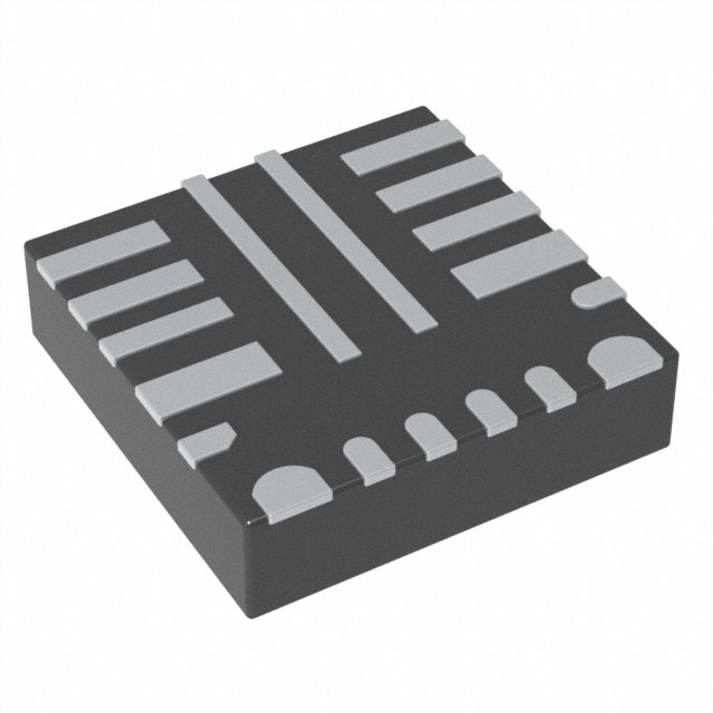


 工商网监
湘ICP备2023018690号
工商网监
湘ICP备2023018690号
