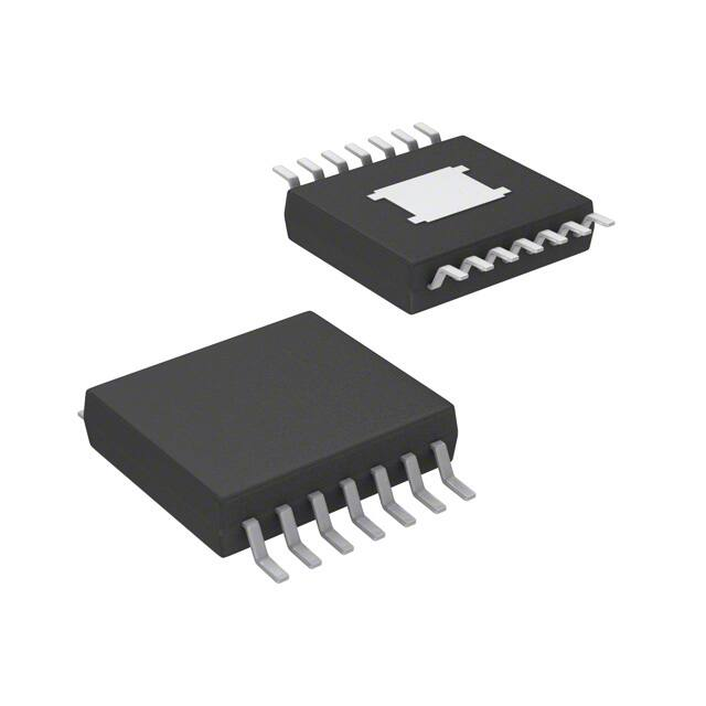
TPS54525
SLVSB82B – MAY 2012 – REVISEDTPS54525
APRIL 2021
SLVSB82B – MAY 2012 – REVISED APRIL 2021
www.ti.com
4.5V to 18V Input, 5.5-A Synchronous Step-Down Converter
1 Features
•
•
•
•
•
•
•
•
•
•
•
•
3 Description
D-CAP2™ mode enables fast transient response
Low output ripple and allows ceramic output
capacitor
Wide VIN input voltage range: 4.5 V to 18 V
Output voltage range: 0.76 V to 5.5 V
Highly efficient integrated FETs optimized
for lower duty cycle applications
–63 mΩ (high side) and 33 mΩ (low side)
High efficiency, less than 10 μA at shutdown
High initial bandgap reference accuracy
Adjustable soft start
Pre-biased soft start
650-kHz switching frequency (fSW)
Cycle-by-cycle overcurrent limit
Power good output
2 Applications
•
Wide range of applications for low voltage system
– Digital TV power supply
– High definition Blu-ray Disc™ players
– Networking home terminal
– Digital set top box (STB)
The TPS54525 is an adaptive on-time D-CAP2™
mode synchronous buck converter. The TPS54525
enables system designers to complete the suite
of various end equipment’s power bus regulators
with a cost effective, low component count, low
standby current solution. The main control loop for
the TPS54525 uses the D-CAP2™ mode control
which provides a very fast transient response with no
external compensation components. The TPS54525
also has a proprietary circuit that enables the device
to adopt to both low equivalent series resistance
(ESR) output capacitors, such as POSCAP or SPCAP, and ultra-low ESR ceramic capacitors. The
device operates from 4.5-V to 18-V VIN input. The
output voltage can be programmed between 0.76 V
and 5.5 V. The device also features an adjustable soft
start time and a power good function. The TPS54525
is available in the 14-pin HTSSOP package, and
designed to operate from –40°C to 85°C.
Device Information
PART NUMBER
PACKAGE
BODY SIZE
TPS54525
HTSSOP
5.00 mm × 6.40 mm
U1
TPS54525
VO (50 mV/div ac coupled)
IOUT (2A/div)
Slew Rate (0.35A/µsec)
Time Scale (100µsec/div)
An©IMPORTANT
NOTICEIncorporated
at the end of this data sheet addresses availability, warranty, changes, use in
safety-critical
applications,
Copyright
2021 Texas Instruments
Submit
Document
Feedback
intellectual property matters and other important disclaimers. PRODUCTION DATA.
Product Folder Links: TPS54525
1
�TPS54525
www.ti.com
SLVSB82B – MAY 2012 – REVISED APRIL 2021
Table of Contents
1 Features............................................................................1
2 Applications..................................................................... 1
3 Description.......................................................................1
4 Revision History.............................................................. 2
5 Pin Configuration and Functions...................................3
6 Specifications.................................................................. 4
6.1 Absolute Maximum Ratings........................................ 4
6.2 ESD Ratings............................................................... 4
6.3 Recommended Operating Conditions.........................5
6.4 Thermal Information....................................................5
6.5 Electrical Characteristics.............................................5
6.6 Typical Characteristics................................................ 7
7 Detailed Description......................................................10
7.1 Overview................................................................... 10
7.2 Functional Block Diagram......................................... 10
7.3 Feature Description...................................................10
7.4 Device Functional Modes..........................................12
8 Application and Implementation.................................. 13
8.1 Application Information............................................. 13
8.2 Typical Application.................................................... 13
9 Power Supply Recommendations................................18
10 Layout...........................................................................19
10.1 Layout Guidelines................................................... 19
10.2 Layout Guidelines................................................... 20
11 Device and Documentation Support..........................22
11.1 Device Support........................................................22
11.2 Receiving Notification of Documentation Updates.. 22
11.3 Support Resources................................................. 22
11.4 Trademarks............................................................. 22
11.5 Electrostatic Discharge Caution.............................. 22
11.6 Glossary.................................................................. 22
4 Revision History
NOTE: Page numbers for previous revisions may differ from page numbers in the current version.
Changes from Revision A (July 2013) to Revision B (April 2021)
Page
• Added the following sections: ESD Ratings, Feature Description, Device Functional Modes, Force CCM
Mode, Application and Implementation, Application Information, Design Requirements, Detailed Design
Procedure, Application Curves, Power Supply Recommendations, Layout, Layout Example, Device and
Documentation Support, and Mechanical, Packaging, and Orderable Information ........................................... 1
• Updated the numbering format for tables, figures, and cross-references throughout the document. ................1
• Updated Equation 2 ......................................................................................................................................... 14
Changes from Revision May 2012 * () to Revision A (July 2013)
Page
• Deleted VFBTH - TA = 0°C to 85°C, VO = 1.05 V, continuous mode from the Electrical Characteristics. ............ 5
• Changed VFBTH - TA = –40°C to 85°C, VO = 1.05 V, continuous mode From: MIN = 751 MAX = 779 mV To:
MIN = 754 MAX = 776 mV in the Electrical Characteristics................................................................................5
• Changed the Over/Under Voltage Protection section. From: "as the high-side MOSFET driver turns off and
the low-side MOSFET turns on" To: "as both the high-side and low-side MOSFET drivers turn off"............... 12
2
Submit Document Feedback
Copyright © 2021 Texas Instruments Incorporated
Product Folder Links: TPS54525
�TPS54525
www.ti.com
SLVSB82B – MAY 2012 – REVISED APRIL 2021
5 Pin Configuration and Functions
PWP PACKAGE
(TOP VIEW)
1
2
3
VO
VFB
VREG5 POWER PAD
VIN2
14
VIN1
13
VBST
12
SW2
11
SW1
10
TPS54525
4
SS
PWP
HTSSOP14
5
GND
6
PG
PGND2 9
7
EN
PGND1
8
Table 5-1. Pin Functions
PIN
NAME
NO.
DESCRIPTION
VO
1
Connect to output of converter. This pin is used for output discharge function.
VFB
2
Converter feedback input. Connect to output voltage with feedback resistor divider.
VREG5
3
5.5 V power supply output. A capacitor (typical 1 µF) should be connected to GND. VREG5 is not active
when EN is low.
SS
4
Soft-start control. An external capacitor should be connected to GND.
GND
5
Signal ground pin
PG
6
Open drain power good output
EN
7
Enable control input. EN is active high and must be pulled up to enable the device.
PGND1, PGND2
SW1, SW2
VBST
VIN1, VIN2
PowerPAD™
8, 9
10, 11
12
Ground returns for low-side MOSFET. Also serve as inputs of current comparators. Connect PGND and
GND strongly together near the IC.
Switch node connection between high-side NFET and low-side NFET. Also serve as inputs to current
comparators.
Supply input for high-side NFET gate driver (boost terminal). Connect capacitor from this pin to
respective SW1, SW2 terminals. An internal PN diode is connected between VREG5 to VBST pin.
13, 14
Power input and connected to high side NFET drain. Supply input for 5-V internal linear regulator for the
control circuitry.
Back side
Thermal pad of the package. Must be soldered to achieve appropriate dissipation. Should be connected
to PGND.
Submit Document Feedback
Copyright © 2021 Texas Instruments Incorporated
Product Folder Links: TPS54525
3
�TPS54525
www.ti.com
SLVSB82B – MAY 2012 – REVISED APRIL 2021
6 Specifications
6.1 Absolute Maximum Ratings
over operating free-air temperature range (unless otherwise noted) (1)
Input voltage range
MIN
MAX
UNIT
VIN1, VIN2 EN
–0.3
20
V
VBST
–0.3
26
V
VBST (10 ns transient)
–0.3
28
V
VBST (vs SW1, SW2)
–0.3
6.5
V
VFB, VO, SS, PG
–0.3
6.5
V
SW1, SW2
–2
20
V
SW1, SW2 (10 ns transient)
–3
22
V
VREG5
–0.3
6.5
V
PGND1, PGND2
–0.3
0.3
V
Voltage from GND to PowerPAD™, Vdiff
–0.2
0.2
V
Operating junction temperature, TJ
–40
150
°C
Output voltage range
(1)
Stresses beyond those listed under absolute maximum ratings may cause permanent damage to the device. These are stress ratings
only, and functional operation of the device at these or any other conditions beyond those indicated under recommended operating
conditions is not implied. Exposure to absolute-maximum-rated conditions for extended periods may affect device reliability.
6.2 ESD Ratings
VALUE
Storage temperature, Tstg
Human-body model (HBM), per ANSI/ESDA/JEDEC
V (ESD)
(1)
(2)
4
Electrostatic discharge
JS-001(1)
Charged-device model (CDM), per JEDEC specification JESD22C101(2)
MIN
MAX
-55
150
-2000
2000
-500
500
UNIT
°C
V
JEDEC document JEP155 states that 500-V HBM allows safe manufacturing with a standard ESD control process.
JEDEC document JEP157 states that 250-V CDM allows safe manufacturing with a standard ESD control process.
Submit Document Feedback
Copyright © 2021 Texas Instruments Incorporated
Product Folder Links: TPS54525
�TPS54525
www.ti.com
SLVSB82B – MAY 2012 – REVISED APRIL 2021
6.3 Recommended Operating Conditions
over operating free-air temperature range (unless otherwise noted)
MIN
VIN
VI
Supply input voltage range
Input voltage range
4.5
18
VBST
–0.3
24
VBST(10 ns transient)
–0.3
27
VBST (vs SW1, SW2)
-0.3
5.7
SS, PG
–0.3
5.7
EN
–0.3
18
VO, VFB
–0.3
5.5
SW1, SW2
–1.8
18
SW1, SW2 (10 ns transient)
VO
MAX
–3
21
PGND1, PGND2
–0.3
0.1
Output voltage range
VREG5
–0.3
5.7
IVREG5
UNIT
V
V
V
IO
Output Current range
0
5
mA
TA
Operating free-air temperature
–40
85
°C
TJ
Operating junction temperature
–40
150
°C
6.4 Thermal Information
TPS54525
THERMAL
METRIC(1)
PWP
UNITS
14 PINS
θJA
Junction-to-ambient thermal resistance
43.7
θJCtop
Junction-to-case (top) thermal resistance
33.1
θJB
Junction-to-board thermal resistance
28.4
ψJT
Junction-to-top characterization parameter
1.3
ψJB
Junction-to-board characterization parameter
28.2
θJCbot
Junction-to-case (bottom) thermal resistance
4.7
°C/W
6.5 Electrical Characteristics
over operating free-air temperature range, VIN = 12V (unless otherwise noted)
PARAMETER
TEST CONDITIONS
MIN
TYP
MAX
UNIT
SUPPLY CURRENT
IVIN
Operating - non-switching supply current
VIN current, TA = 25°C, EN = 5 V,
VVFB = 0.8 V
900
1400
μA
IVINSDN
Shutdown supply current
VIN current, TA = 25°C, EN = 0 V
3.6
10
μA
LOGIC THRESHOLD
VENH
EN high-level input voltage
VENL
EN low-level input voltage
REN
EN pin resistance to GND
1.6
V
0.6
V
VEN = 12 V
220
440
880
kΩ
TA = 25°C, VO = 1.05 V, continuous mode
757
765
773
TA = –40°C to 85°C, VO = 1.05 V, continuous
mode(1)
754
VFB VOLTAGE AND DISCHARGE RESISTANCE
VFBTH
VFB threshold voltage
IVFB
VFB input current
VVFB = 0.8 V, TA = 25°C
RDischg
VO discharge resistance
VEN = 0 V, VO = 0.5 V, TA = 25°C
776
mV
0
±0.15
μA
50
100
Ω
VREG5 OUTPUT
Submit Document Feedback
Copyright © 2021 Texas Instruments Incorporated
Product Folder Links: TPS54525
5
�TPS54525
www.ti.com
SLVSB82B – MAY 2012 – REVISED APRIL 2021
over operating free-air temperature range, VIN = 12V (unless otherwise noted)
PARAMETER
VVREG5
VREG5 output voltage
TEST CONDITIONS
TA = 25°C, 6.0 V < VIN < 18 V,
0 < IVREG5 < 5 mA
VVREG5
VREG5 Line regulation
6.0 V < VIN < 18 V, IVREG5 = 5 mA
VVREG5
VREG5 Load regulation
0 mA < IVREG5 < 5 mA
IVREG5
VREG5 Output current
VIN = 6 V, VVREG5 = 4 V, TA = 25°C
MIN
TYP
MAX
UNIT
5.2
5.5
5.7
V
20
mV
100
mV
60
mA
MOSFET
Rdsonh
High side switch resistance
TA = 25°C, VBST - VSW1,2 = 5.5 V
63
mΩ
Rdsonl
Low side switch resistance
TA = 25°C
33
mΩ
CURRENT LIMIT
Iocl
Current limit
LOUT = 1.5 μH(1)
6.1
6.9
8.4
A
THERMAL SHUTDOWN
TSDN
Thermal shutdown threshold
Shutdown temperature (1)
Hysteresis
165
(1)
°C
35
ON-TIME TIMER CONTROL
TON
On time
VIN = 12 V, VO = 1.05 V
155
TOFF(MIN)
Minimum off time
TA = 25°C, VVFB = 0.7 V
260
330
ns
ns
7.8
μA
SOFT START
ISSC
SS charge current
VSS = 1 V
4.2
6.0
ISSD
SS discharge current
VSS = 0.5 V
0.1
0.2
VVFB rising (good)
85
90
mA
POWER GOOD
VTHPG
PG threshold
IPG
PG sink current
VVFB falling (fault)
VPG = 0.5 V
95
%
85
%
2.5
5
mA
120
125
OUTPUT UNDERVOLTAGE AND OVERVOLTAGE PROTECTION
VOVP
Output OVP trip threshold
TOVPDEL
Output OVP prop delay
VUVP
Output UVP trip threshold
TUVPDEL
Output UVP delay
TUVPEN
Output UVP enable delay
OVP detect
130
10
UVP detect
60
Hysteresis
Relative to soft-start time
65
%
μs
70
%
10
%
0.25
ms
x 1.7
UVLO
Wake up VREG5 voltage
VUVLO
(1)
6
UVLO threshold
3.31
3.61
3.91
Fall VREG5 voltage
2.82
3.12
3.42
Hysteresis VREG5 voltage
0.37
0.49
0.61
V
Not production tested.
Submit Document Feedback
Copyright © 2021 Texas Instruments Incorporated
Product Folder Links: TPS54525
�TPS54525
www.ti.com
SLVSB82B – MAY 2012 – REVISED APRIL 2021
6.6 Typical Characteristics
1200
12
1000
10
Supply Current−Shutdown Current (µA)
Supply Current (µA)
VIN = 12 V, TA = 25 °C (unless otherwise noted)
800
600
400
200
8
6
4
2
VIN = 12 V
0
−50
0
50
100
Junction Temperature (°C)
VIN = 12 V
0
−50
150
0
50
100
Junction Temperature (°C)
150
G001
Figure 6-1. VIN Current vs Junction Temperature
G002
Figure 6-2. VIN Shutdown Current vs Junction
Temperature
1.09
50
VO = 1.05 V
45
1.08
40
Output Voltage (V)
EN Input Current (µA)
35
30
25
20
15
10
1.07
1.06
1.05
1.04
VIN = 5 V
VIN = 12 V
VIN = 18 V
5
VIN = 12 V
0
0
5
10
EN Input Voltage (V)
15
20
1.03
0
0.5
1
1.5
2 2.5 3 3.5
Output Current (A)
G002
Figure 6-3. EN Current vs EN Voltage
4
4.5
5
5.5
G004
Figure 6-4. 1.05-V Output Voltage vs Output
Current
1.07
VO (50 mV/div ac coupled)
Output Voltage (V)
1.06
IOUT (2A/div)
1.05
1.04
Slew Rate (0.35A/µsec)
IO = 0 A
IO = 1 A
1.03
0
5
10
Input Voltage (V)
15
Time Scale (100µsec/div)
20
G005
Figure 6-5. 1.05-V Output Voltage vs Input Voltage
Figure 6-6. 1.05-V, 50-mA to 5.5-A Load Transient
Response
Submit Document Feedback
Copyright © 2021 Texas Instruments Incorporated
Product Folder Links: TPS54525
7
�TPS54525
www.ti.com
SLVSB82B – MAY 2012 – REVISED APRIL 2021
100
EN (10 V/div)
90
80
70
Efficiency (%)
VREG5 (5 V/div)
VO (500 mV/div)
60
50
40
30
PG (5 V/div)
20
VOUT = 1.8 V
VOUT = 2.5 V
VOUT = 3.3 V
10
0
0.0
0.5
1.0
1.5
2.0 2.5 3.0 3.5
Output Current (A)
4.0
4.5
5.0
5.5
G005
Figure 6-7. Start-Up Waveform
Figure 6-8. Efficiency vs Output Current
800
800
750
700
Switching Frequency (kHz)
Switching Frequency (kHz)
700
600
500
600
550
500
VOUT = 1.05 V
VOUT = 1.8 V
VOUT = 3.3 V
400
650
0
5
10
Input Voltage (V)
15
VOUT = 1.05 V
VOUT = 1.8 V
VOUT = 3.3 V
450
20
400
0
0.5
1
1.5
2 2.5 3 3.5
Output Current (A)
4
G006
Figure 6-9. Switching Frequency vs Input Voltage
(IO = 1 A)
5
5.5
G007
Figure 6-10. Switching Frequency vs Output
Current
VO = 1.05 V
VO = 1.05 V
VO (10 mV/div ac coupled)
VIN (50 mV/div ac coupled)
SW (5 V/div)
SW (5 V/div)
Figure 6-11. Voltage Ripple at Outptut (IO = 5.5 A)
8
4.5
Figure 6-12. Voltage Ripple at Input (IO = 5.5 A)
Submit Document Feedback
Copyright © 2021 Texas Instruments Incorporated
Product Folder Links: TPS54525
�TPS54525
www.ti.com
SLVSB82B – MAY 2012 – REVISED APRIL 2021
6
Output Current (A)
5
4
3
2
1
VIN = 12 V
0
−50
−25
VOUT = 1.0 − 4.5 V
VOUT = 5.0 V
VOUT = 5.5 V
0
25
50
Ambient Temperature (°C)
75
100
G008
Figure 6-13. Output Current vs Ambient Temperature
Submit Document Feedback
Copyright © 2021 Texas Instruments Incorporated
Product Folder Links: TPS54525
9
�TPS54525
www.ti.com
SLVSB82B – MAY 2012 – REVISED APRIL 2021
7 Detailed Description
7.1 Overview
The TPS54525 is a 5.5-A synchronous step-down (buck) converter with two integrated N-channel MOSFETs. It
operates using D-CAP2™ mode control. The fast transient response of D-CAP2™ control reduces the output
capacitance required to meet a specific level of performance. Proprietary internal circuitry allows the use of low
ESR output capacitors including ceramic and special polymer types.
7.2 Functional Block Diagram
-35%
UV
14
OV
1
VO
13
VIN
VIN2
VIN1
+25%
VREG5
12
Control logic
VBST
Ref
SS
1 shot
11
2
VFB
XCON
10
SGND
SW2
VREG5
VREG5
Ceramic
Capacitor
3
SS
1uF
VO
SW1
9
PGND2
4
8
Softstart
PGND
5
OCP
PGND
GND
SGND
PG
Ref
VIN
6
-10%
UV
VREG5
EN
7
PGND1
SW
SS
EN
Logic
OV
UVLO
UVLO
Protection
Logic
TSD
REF
Ref
7.3 Feature Description
7.3.1 PWM Operation
The main control loop of the TPS54525 is an adaptive on-time pulse width modulation (PWM) controller that
supports a proprietary D-CAP2™ mode control. D-CAP2™ mode control combines constant on-time control with
an internal compensation circuit for pseudo-fixed frequency and low external component count configuration with
both low ESR and ceramic output capacitors. It is stable even with virtually no ripple at the output.
At the beginning of each cycle, the high-side MOSFET is turned on. This MOSFET is turned off after internal
one shot timer expires. This one shot is set by the converter input voltage, VIN, and the output voltage, VO, to
maintain a pseudo-fixed frequency over the input voltage range, hence it is called adaptive on-time control. The
one-shot timer is reset and the high-side MOSFET is turned on again when the feedback voltage falls below the
reference voltage. An internal ramp is added to reference voltage to simulate output ripple, eliminating the need
for ESR induced output ripple from D-CAP2™ mode control.
10
Submit Document Feedback
Copyright © 2021 Texas Instruments Incorporated
Product Folder Links: TPS54525
�TPS54525
www.ti.com
SLVSB82B – MAY 2012 – REVISED APRIL 2021
7.3.2 PWM Frequency and Adaptive On-Time Control
TPS54525 uses an adaptive on-time control scheme and does not have a dedicated on board oscillator. The
TPS54525 runs with a pseudo-constant frequency of 650 kHz by using the input voltage and output voltage to
set the on-time one-shot timer. The on-time is inversely proportional to the input voltage and proportional to the
output voltage, therefore, when the duty ratio is VOUT/VIN, the frequency is constant.
7.3.3 Soft Start and Pre-Biased Soft Start
The soft start function is adjustable. When the EN pin becomes high, 6-μA current begins charging the capacitor
which is connected from the SS pin to GND. Smooth control of the output voltage is maintained during start up.
The equation for the slow start time is shown in Equation 1. VFB voltage is 0.765 V and SS pin source current is
6 μA.
t
SS
(ms) =
CSS (nF) x VREF ´1.1
I (mA)
SS
=
CSS (nF) x 0.765 ´1.1
6
(1)
The TPS54525 contains a unique circuit to prevent current from being pulled from the output during startup if
the output is pre-biased. When the soft-start commands a voltage higher than the pre-bias level (internal soft
start becomes greater than feedback voltage VFB), the controller slowly activates synchronous rectification by
starting the first low side FET gate driver pulses with a narrow on-time. It then increments that on-time on a
cycle-by-cycle basis until it coincides with the time dictated by (1-D), where D is the duty cycle of the converter.
This scheme prevents the initial sinking of the pre-bias output, and ensure that the out voltage (VO) starts and
ramps up smoothly into regulation and the control loop is given time to transition from pre-biased start-up to
normal mode operation.
7.3.4 Power Good
The TPS54525 has power-good open drain output. The power good function is activated after soft start has
finished. The power good function becomes active after 1.7 times soft-start time. When the output voltage
is within -10% of the target value, internal comparators detect power good state and the power good signal
becomes high. Rpg resister value ,which is connected between PG and VREG5, is required from 25kΩ to
150kΩ. If the feedback voltage goes under 15% of the target value, the power good signal becomes low.
7.3.5 VREG5
VREG5 is an internally generated voltage source used by the TPS54525. It is derived directly from the input
voltage and is nominally regulated to 5.5 V when the input voltage is above 5.6 V. The output of the VREG5
regulator is the input to the internal UVLO function. VREG5 must be above the UVLO wake up threshold voltage
(3.6 V typical) for the TPS54525 to function. Connect a 1 µF capacitor between pin 3 of the TPS54525 and
power ground for proper regulation of the VREG5 output. The VREG5 output voltage is available for external
use. It is recommended to use no more than 5 mA for external loads. The VREG5 output is disabled when the
TPS54525 EN pin is open or pulled low.
7.3.6 Output Discharge Control
TPS54525 discharges the output when EN is low, or the controller is turned off by the protection functions (OVP,
UVP, UVLO and thermal shutdown). The output is discharged by an internal 50-Ω MOSFET which is connected
from VO to PGND. The internal low-side MOSFET is not turned on during the output discharge operation to
avoid the possibility of causing negative voltage at the output.
7.3.7 Current Protection
The output overcurrent protection (OCP) is implemented using a cycle-by-cycle valley detect control circuit.
The switch current is monitored by measuring the low-side FET switch voltage between the SW pin and GND.
This voltage is proportional to the switch current. To improve accuracy, the voltage sensing is temperature
compensated.
During the on time of the high-side FET switch, the switch current increases at a linear rate determined by VIN,
VOUT, the on-time and the output inductor value. During the on time of the low-side FET switch, this current
Submit Document Feedback
Copyright © 2021 Texas Instruments Incorporated
Product Folder Links: TPS54525
11
�TPS54525
www.ti.com
SLVSB82B – MAY 2012 – REVISED APRIL 2021
decreases linearly. The average value of the switch current is the load current IOUT. If the measured voltage is
above the voltage proportional to the current limit, Then , the device constantly monitors the low-side FET switch
voltage, which is proportional to the switch current, during the low-side on-time.
The converter maintains the low-side switch on until the measured voltage is below the voltage corresponding to
the current limit at which time the switching cycle is terminated and a new switching cycle begins. In subsequent
switching cycles, the on-time is set to a fixed value and the current is monitored in the same manner.
There are some important considerations for this type of overcurrent protection. The load current one half of
the peak-to-peak inductor current higher than the overcurrent threshold. Also when the current is being limited,
the output voltage tends to fall as the demanded load current may be higher than the current available from
the converter. This may cause the output undervoltage protection circuit to be activated. When the over current
condition is removed, the output voltage returns to the regulated value. This protection is non-latching.
7.3.8 Over/Under Voltage Protection
TPS54525 monitors a resistor divided feedback voltage to detect over and under voltage. When the feedback
voltage becomes higher than 125% of the target voltage, the OVP comparator output goes high and the circuit
latches as both the high-side and low-side MOSFET drivers turn off. When the feedback voltage becomes
lower than 65% of the target voltage, the UVP comparator output goes high and an internal UVP delay counter
begins. After 250 μs, the device latches off both internal top and bottom MOSFET. This function is enabled
approximately 1.7 x softstart time.
7.3.9 UVLO Protection
Undervoltage lock out protection (UVLO) monitors the voltage of the VREG5 pin. When the VREG5 voltage is lower
than UVLO threshold voltage, the TPS54525 is shut off. This is protection is non-latching.
7.3.10 Thermal Shutdown
TPS54525 monitors the temperature of itself. If the temperature exceeds the threshold value (typically 165°C),
the device is shut off. This is non-latch protection.
7.4 Device Functional Modes
7.4.1 Forced CCM Mode
The TPS54525 operates in Forced CCM (FCCM) mode, which keeps the converter operating in continuous
current mode during light-load conditions and allows the inductor current to become negative. During FCCM
mode, the switching frequency (FSW) is maintained at an almost constant level over the entire load range, which
is suitable for applications requiring tight control of the switching frequency and output voltage ripple at the cost
of lower efficiency under light load.”
12
Submit Document Feedback
Copyright © 2021 Texas Instruments Incorporated
Product Folder Links: TPS54525
�TPS54525
www.ti.com
SLVSB82B – MAY 2012 – REVISED APRIL 2021
8 Application and Implementation
Note
Information in the following applications sections is not part of the TI component specification,
and TI does not warrant its accuracy or completeness. TI’s customers are responsible for
determining suitability of components for their purposes, as well as validating and testing their design
implementation to confirm system functionality.
8.1 Application Information
Figure 8-1 shows a typical application for TPS54525 with 1.05-V output. This design converts an input voltage
range of 4.5 V to 18 V down to 1.05 V with a maximum output current of 5.5 A.
8.2 Typical Application
U1
TPS54525PWP
Figure 8-1. Schematic Diagram
8.2.1 Design Requirements
For this design example, use the following input parameters:
Table 8-1. Design Parameters
PARAMETER
VALUE
Input voltage range
4.5 V – 18 V
Output voltage
1.05 V
Output current rating
0 A – 5.5 A
Output voltage ripple
7 mVPP (12 VIN / 5.5 A)
8.2.2 Detailed Design Procedure
8.2.2.1 Step By Step Design Procedure
To begin the design process, you must know a few application parameters:
•
•
•
•
•
Input voltage range
Output voltage
Output current
Output voltage ripple
Input voltage ripple
Submit Document Feedback
Copyright © 2021 Texas Instruments Incorporated
Product Folder Links: TPS54525
13
�TPS54525
www.ti.com
SLVSB82B – MAY 2012 – REVISED APRIL 2021
8.2.2.2 Output Voltage Resistors Selection
The output voltage is set with a resistor divider from the output node to the VFB pin. It is recommended to use
1% tolerance or better divider resistors. Start by using Equation 2 to calculate VOUT.
To improve efficiency at very light loads consider using larger value resistors, too high of resistance will be more
susceptible to noise and voltage errors from the VFB input current will be more noticeable.
§
0.0011 u VOUT _ SET u ¨ 1
©
where VOUT _ SET is t arget VOUT voltage
V OUT
0.7651
R1 ·
R2 ¸¹
(2)
8.2.2.3 Output Filter Selection
The output filter used with the TPS54525 is an LC circuit. This LC filter has double pole at:
FP =
1
2p LOUT ´ COUT
(3)
At low frequencies, the overall loop gain is set by the output set-point resistor divider network and the internal
gain of the TPS54525. The low frequency phase is 180 degrees. At the output filter pole frequency, the gain
rolls off at a -40 dB per decade rate and the phase drops rapidly. D-CAP2™ introduces a high frequency zero
that reduces the gain roll off to -20 dB per decade and increases the phase to 90 degrees one decade above
the zero frequency. The inductor and capacitor selected for the output filter must be selected so that the double
pole of Equation 3 is located below the high frequency zero but close enough that the phase boost provided be
the high frequency zero provides adequate phase margin for a stable circuit. To meet this requirement use the
values recommended in Table 8-2
Table 8-2. Recommended Component Values
C4 (pF)(1)
Output Voltage (V)
R1 (kΩ)
R2 (kΩ)
1
6.81
22.1
1.0 - 1.5
22 - 68
1.05
8.25
22.1
1.0 - 1.5
22 - 68
1.2
12.7
22.1
1.0 - 1.5
22 - 68
1.5
21.5
22.1
1.5
22 - 68
1.8
30.1
22.1
5 - 22
1.5
22 - 68
2.5
49.9
22.1
5 - 22
2.2
22 - 68
3.3
73.2
22.1
5 - 22
2.2
22 - 68
5
124
22.1
5 - 22
3.3
22 - 68
(1)
L1 (µH)
C8 + C9 (µF)
Optional
For higher output voltages at or above 1.8 V, additional phase boost can be achieved by adding a feed forward
capacitor (C4) in parallel with R1.
Since the DC gain is dependent on the output voltage, the required inductor value will increase as the output
voltage increases. For higher output voltages at or above 1.8 V, additional phase boost can be achieved by
adding a feed forward capacitor (C4) in parallel with R1
The inductor peak-to-peak ripple current, peak current and RMS current are calculated using Equation 4,
Equation 5 and Equation 6. The inductor saturation current rating must be greater than the calculated peak
current and the RMS or heating current rating must be greater than the calculated RMS current. Use 650 kHz for
fSW.
Use 650 kHz for fSW. Make sure the chosen inductor is rated for the peak current of Equation 5 and the RMS
current of Equation 6.
14
Submit Document Feedback
Copyright © 2021 Texas Instruments Incorporated
Product Folder Links: TPS54525
�TPS54525
www.ti.com
SLVSB82B – MAY 2012 – REVISED APRIL 2021
VOUT VIN (max) - VOUT
•
Ilp - p = V
L •f
(4)
Ilp - p
Ilpeak = IO +
2
(5)
IN (max)
ILo(RMS) =
O
SW
−
1
√I
O
2
+ − Ilp - p2
12
(6)
For this design example, the calculated peak current is 6.01 A and the calculated RMS current is 5.5 A. The
inductor used is a TDK SPM6530-1R5M100 with a peak current rating of 11.5 A and an RMS current rating of 11
A.
The capacitor value and ESR determines the amount of output voltage ripple. The TPS54525 is intended for use
with ceramic or other low ESR capacitors. Recommended values range from 22uF to 68uF. Use Equation 7 to
determine the required RMS current rating for the output capacitor.
VOUT • (VIN - VOUT)
ICO(RMS) =−
−
√12 • VIN • LO • fSW
(7)
For this design two TDK C3216X5R0J226M 22uF output capacitors are used. The typical ESR is 2 mΩ each.
The calculated RMS current is 0.284 A and each output capacitor is rated for 4A.
8.2.2.4 Input Capacitor Selection
The TPS54525 requires an input decoupling capacitor and a bulk capacitor is needed depending on the
application. A ceramic capacitor over 10 μF is recommended for the decoupling capacitor. An additional 0.1
µF capacitor from pin 14 to ground is recommended to improve the EMI performance. The capacitor voltage
rating needs to be greater than the maximum input voltage.
8.2.2.5 Bootstrap Capacitor Selection
A 0.1 µF ceramic capacitor must be connected between the VBST to SW pin for proper operation. It is
recommended to use a ceramic capacitor.
8.2.2.6 VREG5 Capacitor Selection
A 1.0 µF ceramic capacitor must be connected between the VREG5 to GND pin for proper operation. It is
recommended to use a ceramic capacitor.
Submit Document Feedback
Copyright © 2021 Texas Instruments Incorporated
Product Folder Links: TPS54525
15
�TPS54525
www.ti.com
SLVSB82B – MAY 2012 – REVISED APRIL 2021
8.2.3 Application Curves
1.09
1.07
VO = 1.05 V
1.08
Output Voltage (V)
Output Voltage (V)
1.06
1.07
1.06
1.05
1.05
1.04
1.04
1.03
VIN = 5 V
VIN = 12 V
VIN = 18 V
0
0.5
1
1.5
2 2.5 3 3.5
Output Current (A)
4
4.5
5
IO = 0 A
IO = 1 A
1.03
5.5
0
5
10
Input Voltage (V)
15
20
G004
Figure 8-2. 1.05-V Output Voltage vs Output
Current
G005
Figure 8-3. 1.05-V Output Voltage vs Input Voltage
EN (10 V/div)
VO (50 mV/div ac coupled)
VREG5 (5 V/div)
VO (500 mV/div)
IOUT (2A/div)
PG (5 V/div)
Slew Rate (0.35A/µsec)
Time Scale (100µsec/div)
Figure 8-4. 1.05-V, 50-mA to 5.5-A Load Transient
Response
Figure 8-5. Start-Up Waveform
800
100
90
80
Switching Frequency (kHz)
700
Efficiency (%)
70
60
50
40
30
600
500
20
VOUT = 1.8 V
VOUT = 2.5 V
VOUT = 3.3 V
10
0
0.0
0.5
1.0
1.5
2.0 2.5 3.0 3.5
Output Current (A)
4.0
4.5
5.0
VOUT = 1.05 V
VOUT = 1.8 V
VOUT = 3.3 V
5.5
400
G005
Figure 8-6. Efficiency vs Output Current
16
0
5
10
Input Voltage (V)
15
20
G006
Figure 8-7. Switching Frequency vs Input Voltage
(IO = 1 A)
Submit Document Feedback
Copyright © 2021 Texas Instruments Incorporated
Product Folder Links: TPS54525
�TPS54525
www.ti.com
SLVSB82B – MAY 2012 – REVISED APRIL 2021
800
VO = 1.05 V
VO (10 mV/div ac coupled)
750
Switching Frequency (kHz)
700
650
600
SW (5 V/div)
550
500
VOUT = 1.05 V
VOUT = 1.8 V
VOUT = 3.3 V
450
400
0
0.5
1
1.5
2 2.5 3 3.5
Output Current (A)
4
4.5
5
5.5
G007
Figure 8-8. Switching Frequency vs Output Current
Figure 8-9. Voltage Ripple at Outptut (IO = 5.5 A)
6
VO = 1.05 V
VIN (50 mV/div ac coupled)
Output Current (A)
5
SW (5 V/div)
4
3
2
1
VIN = 12 V
0
−50
Figure 8-10. Voltage Ripple at Input (IO = 5.5 A)
−25
VOUT = 1.0 − 4.5 V
VOUT = 5.0 V
VOUT = 5.5 V
0
25
50
Ambient Temperature (°C)
75
100
G008
Figure 8-11. Output Current vs Ambient
Temperature
Submit Document Feedback
Copyright © 2021 Texas Instruments Incorporated
Product Folder Links: TPS54525
17
�TPS54525
www.ti.com
SLVSB82B – MAY 2012 – REVISED APRIL 2021
9 Power Supply Recommendations
The device is designed to operate from an input voltage supply range between 4.5 V and 18 V. This input supply
should be well regulated. If the input supply is located more than a few inches from the TPS54525 converter
additional bulk capacitance may be required in addition to the ceramic bypass capacitors. An electrolytic
capacitor with a value of 100 μF is a typical choice.
18
Submit Document Feedback
Copyright © 2021 Texas Instruments Incorporated
Product Folder Links: TPS54525
�TPS54525
www.ti.com
SLVSB82B – MAY 2012 – REVISED APRIL 2021
10 Layout
10.1 Layout Guidelines
•
•
•
•
•
•
•
•
•
•
•
•
•
•
Keep the input switching current loop as small as possible.
Keep the SW node as physically small and short as possible to minimize parasitic capacitance and
inductance and to minimize radiated emissions. Kelvin connections should be brought from the output to
the feedback pin of the device.
Keep analog and non-switching components away from switching components.
Make a single point connection from the signal ground to power ground.
Do not allow switching current to flow under the device.
VREG5 capacitor should be placed near the device, and connected PGND.
Output capacitor should be connected to a broad pattern of the PGND.
Voltage feedback loop should be as short as possible, and preferably with ground shield.
Lower resistor of the voltage divider which is connected to the VFB pin should be tied to SGND.
Providing sufficient via is preferable for VIN, SW and PGND connection.
PCB pattern for VIN and SW should be as broad as possible.
VIN Capacitor should be placed as near as possible to the device.
The top side power ground (PGND) copper fill area near the IC should be as large as possible. This will aid in
thermal dissipation as well lower conduction losses in the ground return
Exposed pad of device must be connected to PGND with solder. The PGND area under the IC should be
as large as possible and completely cover the exposed thermal pad. The bottom side of the board should
contain a large copper area under the device that is directly connected to the exposed area with small
diameter vias. Small diameter vias will prevent solder from being drawn away from the exposed thermal pad.
Any additional internal layers should also contain copper ground areas under the device and be connected to
the thermal vias.
Submit Document Feedback
Copyright © 2021 Texas Instruments Incorporated
Product Folder Links: TPS54525
19
�TPS54525
www.ti.com
SLVSB82B – MAY 2012 – REVISED APRIL 2021
10.2 Layout Guidelines
VIN
Additional
Thermal
Vias
FEEDBACK
RESISTORS
VOUT
BIAS
CAP
Connection to
POWER GROUND
on internal or
bottom layer
SLOW
START
CAP
ANALOG
GROUND
TRACE
To Enable
Control
VIN
INPUT
BYPASS
CAPACITOR
VIN OVER
CURRENT
STABILITY
CAPACITOR
EXPOSED
POWERPAD
AREA
VIN2
VFB
VIN1
VREG5
VBST
SS
SW1
GND
SW2
PG
PGND1
EN
PGND2
BOOST
CAPACITOR
OUTPUT
INDUCTOR
VOUT
OUTPUT
FILTER
CAPACITOR
Additional
Thermal
Vias
POWER GROUND
VIA to Ground Plane
Etch on Bottom Layer
or Under Component
Figure 10-1. PCB Layout
10.2.1 Thermal Considerations
This PowerPad™ package incorporates an exposed thermal pad that is designed to be directly to an external
heartsick. The thermal pad must be soldered directly to the printed board (PCB). After soldering, the PCB can
be used as a heartsick. In addition, through the use of thermal vias, the thermal pad can be attached directly to
the appropriate copper plane shown in the electrical schematic for the device, or alternatively, can be attached to
a special heartsick structure designed into the PCB. This design optimizes the heat transfer from the integrated
circuit (IC).
For additional information on the PowerPAD™ package and how to use the advantage of its heat dissipating
abilities, refer to Technical Brief, PowerPAD™ Thermally Enhanced Package, Texas Instruments Literature No.
SLMA002 and Application Brief, PowerPAD™ Made Easy, Texas Instruments Literature No. SLMA004.
The exposed thermal pad dimensions for this package are shown in the following illustration.
20
Submit Document Feedback
Copyright © 2021 Texas Instruments Incorporated
Product Folder Links: TPS54525
�TPS54525
www.ti.com
SLVSB82B – MAY 2012 – REVISED APRIL 2021
8
14
Thermal Pad
2.46
°
7
1
2.31
Figure 10-2. Thermal Pad Dimensions
Submit Document Feedback
Copyright © 2021 Texas Instruments Incorporated
Product Folder Links: TPS54525
21
�TPS54525
www.ti.com
SLVSB82B – MAY 2012 – REVISED APRIL 2021
11 Device and Documentation Support
TI offers an extensive line of development tools. Tools and software to evaluate the performance of the device,
generate code, and develop solutions are listed below.
11.1 Device Support
11.1.1 Third-Party Products Disclaimer
TI'S PUBLICATION OF INFORMATION REGARDING THIRD-PARTY PRODUCTS OR SERVICES DOES NOT
CONSTITUTE AN ENDORSEMENT REGARDING THE SUITABILITY OF SUCH PRODUCTS OR SERVICES
OR A WARRANTY, REPRESENTATION OR ENDORSEMENT OF SUCH PRODUCTS OR SERVICES, EITHER
ALONE OR IN COMBINATION WITH ANY TI PRODUCT OR SERVICE.
11.2 Receiving Notification of Documentation Updates
To receive notification of documentation updates, navigate to the device product folder on ti.com. Click on
Subscribe to updates to register and receive a weekly digest of any product information that has changed. For
change details, review the revision history included in any revised document.
11.3 Support Resources
TI E2E™ support forums are an engineer's go-to source for fast, verified answers and design help — straight
from the experts. Search existing answers or ask your own question to get the quick design help you need.
Linked content is provided "AS IS" by the respective contributors. They do not constitute TI specifications and do
not necessarily reflect TI's views; see TI's Terms of Use.
11.4 Trademarks
D-CAP2™ and TI E2E™ are trademarks of Texas Instruments.
Blu-ray Disc™ is a trademark of Blu-ray Disc Association.
All trademarks are the property of their respective owners.
11.5 Electrostatic Discharge Caution
This integrated circuit can be damaged by ESD. Texas Instruments recommends that all integrated circuits be handled
with appropriate precautions. Failure to observe proper handling and installation procedures can cause damage.
ESD damage can range from subtle performance degradation to complete device failure. Precision integrated circuits may
be more susceptible to damage because very small parametric changes could cause the device not to meet its published
specifications.
11.6 Glossary
TI Glossary
22
This glossary lists and explains terms, acronyms, and definitions.
Submit Document Feedback
Copyright © 2021 Texas Instruments Incorporated
Product Folder Links: TPS54525
�PACKAGE OPTION ADDENDUM
www.ti.com
29-Mar-2021
PACKAGING INFORMATION
Orderable Device
Status
(1)
Package Type Package Pins Package
Drawing
Qty
Eco Plan
(2)
Lead finish/
Ball material
MSL Peak Temp
Op Temp (°C)
Device Marking
(3)
(4/5)
(6)
TPS54525PWP
ACTIVE
HTSSOP
PWP
14
90
RoHS & Green
NIPDAU
Level-2-260C-1 YEAR
-40 to 85
PS54525
TPS54525PWPR
ACTIVE
HTSSOP
PWP
14
2000
RoHS & Green
NIPDAU
Level-2-260C-1 YEAR
-40 to 85
PS54525
(1)
The marketing status values are defined as follows:
ACTIVE: Product device recommended for new designs.
LIFEBUY: TI has announced that the device will be discontinued, and a lifetime-buy period is in effect.
NRND: Not recommended for new designs. Device is in production to support existing customers, but TI does not recommend using this part in a new design.
PREVIEW: Device has been announced but is not in production. Samples may or may not be available.
OBSOLETE: TI has discontinued the production of the device.
(2)
RoHS: TI defines "RoHS" to mean semiconductor products that are compliant with the current EU RoHS requirements for all 10 RoHS substances, including the requirement that RoHS substance
do not exceed 0.1% by weight in homogeneous materials. Where designed to be soldered at high temperatures, "RoHS" products are suitable for use in specified lead-free processes. TI may
reference these types of products as "Pb-Free".
RoHS Exempt: TI defines "RoHS Exempt" to mean products that contain lead but are compliant with EU RoHS pursuant to a specific EU RoHS exemption.
Green: TI defines "Green" to mean the content of Chlorine (Cl) and Bromine (Br) based flame retardants meet JS709B low halogen requirements of