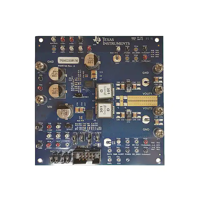
User's Guide
SLUUBH4 – October 2016
Using the TPS546C23 Two Separated, Single-Phase
Evaluation Module
The TPS546C23EVM1-746 evaluation module (EVM) uses two TPS546C23 devices. The TPS546C23
device is a stackable synchronous buck with PMBus interface that can operate from a nominal 4.5-V to
18-V supply. The device allows programming and monitoring via the PMBus interface.
Two TPS546C23 devices are configured as two separated single phase buck converter in factory default;
the negative terminals of the two outputs are connected together internally, while the positive terminals are
separated.
1
2
3
4
5
6
7
8
9
10
Contents
Description .................................................................................................................... 3
1.1
Typical Applications ................................................................................................ 3
1.2
Features .............................................................................................................. 3
Electrical Performance Specifications ..................................................................................... 4
Schematic ..................................................................................................................... 4
Test Setup .................................................................................................................... 6
4.1
Test and Configuration Software ................................................................................. 6
4.2
Test Equipment ..................................................................................................... 6
4.3
Recommended Test Setup ........................................................................................ 7
4.4
List of Test Points, Jumpers and Connectors ................................................................... 8
EVM Configuration Using the Fusion GUI .............................................................................. 10
5.1
Configuration Procedure ......................................................................................... 10
Test Procedure ............................................................................................................. 12
6.1
Line and Load Regulation and Efficiency Measurement Procedure ........................................ 12
6.2
Control Loop Gain and Phase Measurement Procedure .................................................... 12
6.3
Efficiency Measurement .......................................................................................... 13
Performance Data and Typical Characteristic Curves................................................................. 14
7.1
Efficiency ........................................................................................................... 14
7.2
Load Regulation ................................................................................................... 14
7.3
Line Regulation .................................................................................................... 15
7.4
Transient Response............................................................................................... 15
7.5
Output Ripple ...................................................................................................... 15
7.6
Control On .......................................................................................................... 16
7.7
Control Off .......................................................................................................... 17
7.8
Control On under Pre-bias ....................................................................................... 17
7.9
Overcurrent Protection............................................................................................ 18
7.10 Control Loop Bode Plot ........................................................................................... 18
7.11 Thermal Image..................................................................................................... 20
EVM Assembly Drawing and PCB Layout .............................................................................. 21
Bill of Materials ............................................................................................................. 26
Screenshots ................................................................................................................. 28
10.1 Fusion GUI Screenshots ......................................................................................... 28
List of Figures
1
TPS546C23EVM1-746 Schematic ........................................................................................ 5
2
TPS546C23EVM1-746 EVM Recommended Test Set Up For Output #1 ........................................... 7
SLUUBH4 – October 2016
Submit Documentation Feedback
Using the TPS546C23 Two Separated, Single-Phase Evaluation Module
Copyright © 2016, Texas Instruments Incorporated
1
�www.ti.com
3
TPS546C23EVM1-746 EVM Recommended Test Set Up For Output #2 ........................................... 7
4
Tip and Barrel Measurement ............................................................................................... 8
5
Efficiency of 0.9-V Output vs Line and Load
6
Load Regulation of 0.9-V Output ......................................................................................... 14
7
Line Regulation of 0.9-V Output (Different Board) ..................................................................... 15
8
Transient Response of 0.9-V Output at 12 VIN, Transient is 10 A to 30 A, 0.2 A/µs .............................. 15
9
Output Ripple and SW Node of 0.9-V Output at 12 VIN, 0-A Output................................................. 15
10
Output Ripple and SW Node of 0.9-V Output at 12 VIN, 35-A Output
11
Start up from Control, 0.9-V Output at 12 VIN, 0-A Output ............................................................ 16
12
Start up from Control, 0.9-V Output at 12 VIN, 35-A Output
13
Soft Stop from Control, 0.9-V Output at 12 VIN, 35-A Output ......................................................... 17
14
0.6-V Pre-bias start up from Control, 0.9-V Output at 12 VIN, 0-A Output .......................................... 17
15
Overcurrent Protection, 0.9-V Output at 12 VIN, 35-A Output (OC_Fault threshold is modified to 35A) ........ 18
16
Bode Plot at 0.9-V Output at 12 VIN, 0-A Output
17
18
19
20
21
22
23
24
25
26
27
28
29
30
31
32
33
34
35
36
37
...........................................................................
..............................................
..........................................................
......................................................................
Bode Plot at 0.9-V Output at 12 VIN, 35-A Output......................................................................
Thermal Image .............................................................................................................
Thermal Image .............................................................................................................
TPS546C23EVM1-746 EVM 3D Top View .............................................................................
TPS546C23EVM1-746 EVM Top Layer Assembly Drawing (Top View) ...........................................
TPS546C23EVM1-746 EVM Bottom Assembly Drawing (Bottom View) ...........................................
TPS546C23EVM1-746 EVM Top Copper (Top View).................................................................
TPS546C23EVM1-746 EVM Internal Layer 1 (Top View) ............................................................
TPS546C23EVM1-746 EVM Internal Layer 2 (Top View) ............................................................
TPS546C23EVM1-746 EVM Internal Layer 3 (Top View) ............................................................
TPS546C23EVM1-746 EVM Internal Layer 4 (Top View) ............................................................
TPS546C23EVM1-746 EVM Bottom Copper (Top View) .............................................................
Select Device Scanning Mode............................................................................................
Configure- Limits and On/Off ............................................................................................
ON/OFF Control Pop-up...................................................................................................
Configure - Advanced .....................................................................................................
Configure - SMBALERT # Mask .........................................................................................
Configure - Device Info ....................................................................................................
Configure - All Config ......................................................................................................
Monitor Screen .............................................................................................................
Status Screen ...............................................................................................................
14
16
16
18
19
20
20
21
21
22
22
23
23
24
24
25
28
29
30
31
32
33
34
35
36
List of Tables
2
1
TPS546C23EVM1-746 Electrical Performance Specifications ........................................................ 4
2
Test Point Functions
3
Jumpers ....................................................................................................................... 9
4
Connector Functions ........................................................................................................ 9
5
Key Factory Configuration Parameters .................................................................................. 10
6
List of Test Points for Loop Response Measurements ................................................................ 12
7
Test Points for Better Efficiency Measurements ....................................................................... 13
8
TPS546C23EVM1-746 Components List
........................................................................................................
..............................................................................
Using the TPS546C23 Two Separated, Single-Phase Evaluation Module
Copyright © 2016, Texas Instruments Incorporated
8
26
SLUUBH4 – October 2016
Submit Documentation Feedback
�Description
www.ti.com
1
Description
The TPS546C23EVM1-746 includes two separated buck converters. It uses a nominal 12-V bus to
produce two regulated 0.9-V outputs at up to 35 A of load current. The TPS546C23EVM1-746 is designed
to demonstrate the TPS546C23 in a typical single phase low output voltage application while providing a
number of test points to evaluate the performance of the device. The TPS546C23EVM1-746 is NOT
recommended to be modified to two-phase interleaving buck converter by changing the bill of materials
(BOM). Refer to the TPS546C23 (SLUSCC7) datasheet for more information on multi-phase configuration.
1.1
Typical Applications
•
•
•
•
•
•
•
1.2
High-density power solutions
Wireless infrastructure
Switcher
Router Network
Server
Storage
Smart power systems
Features
•
•
•
Two regulated 0.9-V outputs up to 35-A DC steady-state output current
Both outputs are marginable and trimmable via the PMBus interface
– Programmable UVLO, soft-start, and enable via the PMBus interface
– Programmable overcurrent warning and fault limits and programmable response to faults via the
PMBus interface
– Programmable overvoltage and undervoltage warning and fault limits and programmable response
to faults via the PMBus interface
– Programmable turn-on and turn-off delays
Convenient test points for probing critical waveforms
All trademarks are the property of their respective owners.
SLUUBH4 – October 2016
Submit Documentation Feedback
Using the TPS546C23 Two Separated, Single-Phase Evaluation Module
Copyright © 2016, Texas Instruments Incorporated
3
�Electrical Performance Specifications
2
www.ti.com
Electrical Performance Specifications
Table 1 lists the electrical performance specifications under room temperature 25°C.
Table 1. TPS546C23EVM1-746 Electrical Performance Specifications
Parameter
Test Conditions
MIN
TYP
MAX
Unit
12
18
V
Input Characteristics
Voltage range
VIN
Maximum input current
VIN = 12 V, IO1 = 35 A, IO2 = 35 A
5
6.5
A
No load input current
VIN = 12 V, IO1 = 0 A, IO2 = 0 A
100
mA
Output voltage, VOUT1
0.9
V
Output voltage, VOUT2
0.9
Output Characteristics
Output load current, IOUT1 (1)
Output load current, IOUT2
0
(1)
0
V
35
A
35
A
Line Regulation: Input voltage = 5 V to 18 V
1%
Output voltage regulation
Load Regulation: Output current = 0 A to 35 A, both
outputs
1%
Output voltage ripple, VOUT1
VIN = 12 V, IOUT1 = 35 A
10
mVpp
Output voltage ripple, VOUT2
VIN = 12 V, IOUT2 = 35 A
10
mVpp
Output Over-current Protection
Threshold
Load current IOUT1, default setting
42
A
Load current IOUT2, default setting
42
A
kHz
Systems Characteristics
Switching frequency
VIN = 12 V
500
(2)
VIN = 12 V, IO1 = 35 A, VOUT2 disabled
84%
Full load efficiency, VOUT2 (2)
VIN = 12 V, IO2 = 35 A, VOUT1 disabled
84%
Operating temperature
Toper
25
°C
U1 PMBUS Address
Programmed by R33 and R35
27
U2 PMBus Address
Programmed by R37 and R36
36
Decim
al
U1 Voltage reference
Default setting of VOUT_COMMAND
600
U2 Voltage reference
Default setting of VOUT_COMMAND
600
U1 Soft-start time (TON_RISE)
Default setting of TON_RISE
3
U2 Soft-start time (TON_RISE)
Default setting of TON_RISE
3
Full load efficiency, VOUT1
PMBUS Interface and Pin-Strapping
(1)
(2)
3
mV
ms
The output current IOUT1 and IOUT2 can be up to 40 A, if the output overcurrent limit (IOUT_OC_FAULT_LIMIT) is set to 45 A.
The efficiency is measured based on Figure 2 and Figure 3 test setups, which includes power loss caused by on board copper
traces.
Schematic
Figure 1 illustrates the TPS546C23EVM1-746 EVM schematic.
4
Using the TPS546C23 Two Separated, Single-Phase Evaluation Module
Copyright © 2016, Texas Instruments Incorporated
SLUUBH4 – October 2016
Submit Documentation Feedback
�Schematic
www.ti.com
LED1
R1
2
1
1.00k
CLK
DNP
CLK_M
1
3
5
7
9
TP3
TP4
DNP
CNTL
DATA SMBA LRT
Green
TP1
CNTL
CLK
2
4
6
8
10
TP2
DNP
DNP
SMBALRT
DATA
J1
JP1
GND
PMBus
CLK_S
DATA_M
VIN = 4.5 - 18 VDC
JP2
JP3
J2
J3
DATA_S
TP5
1546
AVIN1
JP4
TP6
1546
GND
VIN
PVIN1
PVIN2
TP7
TP8
AVIN2
TP9
TP10
R2
R3
0
C1
1µF
0
TP11
C6
6800pF
C7
6800pF
R6
CHA1
1200pF
CHB1
TP14
R9
DNP
10.0k
TP15
TP18
R10
R11
DNP
10.0k
49.9
R17
10.0k
R21
10.0k
C28
CNTL
3
2
1
JP7
150pF
TP25
R25
10.0k
RST/PG1
C33
2.2µF
R34
20.0k
PVIN
PVIN
PVIN
PVIN
PVIN
29
AVIN
35
DIFFO
36
FB
39
JP6
C38
2.2µF
21
22
23
24
25
37
SYNC
C30 1500pF
C39
4.7µF
C40
0.1µF
R33
34.8k
CLK_M
R32
DNP
10.0k
DATA_M
R35
34.8k
Fsw = 500kHz
R38
40.2k
40
C10
22µF
C21
BOOT
7
0.1µF
SW
SW
SW
SW
SW
C13
22µF
R5
0
0
L1
C14
22µF
C15
22µF
SW1
34
ADDR0
2
ADDR1
PMB_CLK
C18
6800pF
8
9
10
11
12
300 nH
Avg1
R18
10.0k
DNP
TP21
3
300nH
Coupled Inductor
DNP
SMB1
R16
49.9
TP20
Avg2
DNP
TP22
DNP
SMB2
R19
10.0k
C26
1000pF
GND
TP23
GND
TP24
AVIN
29
DIFFO
35
FB
36
SYNC
CNTL
RSP_S
GND
21
22
23
24
25
COMP
C31 R23
1µF
1.0
1µF
RSP_M
RSN_M
SW2
SW
SW
SW
SW
SW
PVIN
PVIN
PVIN
PVIN
PVIN
GND
RSN_S
33
RSP
34
RSN
ISHARE
VSHARE
31
ISHARE1
32
VSHARE1
R29
DNP
0
VSHARE
R26
DNP
5.11k
R30
DNP
0
ISHARE R27
DNP
5.11k
ISHARE2
31
VSHARE2
32
28
ADDR0
26
DRGND
38
AGND
PAD
13
14
15
16
17
18
19
20
13
14
15
16
17
18
19
20
41
41
PGND
PGND
PGND
PGND
PGND
PGND
PGND
PGND
2
5
PMB_DATA
4
SMB_ALRT
CHA2
TP17
1.10k
TP13
1200pF
DNP
R12
R13
49.9
10.0k
R14
10.0k
R20
10.0k
C32
JP8
150pF
R24
10.0k
RST/PG2
TP26
3
ADDR1
RT
PGND
PGND
PGND
PGND
PGND
PGND
PGND
PGND
C24
R8
CHB2
TP16
1500pF
3
2
1
CNTL
30
PMB_CLK
RT
JP5
R7
DNP
10.0k
39
27
VSHARE
SYNC
37
40
BP6
ISHARE
PMB_DATA
SMBALRT
C20
1µF
TP12
C27
BP3
RESET/PGD
SMB_ALRT
C19
6800pF
TPS546C23RVFR
BOOT
RESET/PGD
3
C17
6800pF
0.1µF
2
4
R15
49.9
TP19
C29
R22
1.0
CNTL
33
7
DNP
SYNC
RSP
L3
300 nH
COMP
5
C16
22µF
C22
L2
1
C25
1000pF
RSN
6
C5
100µF
R4
8
9
10
11
12
BP6
1
C4
100µF
SLAVE
BP3
JP9
C3
100µF
U2
28
4
C2
100µF
C12
22µF
GND
27
30
C11
22µF
TPS546C23RVFR
U1
1.10k
C9
22µF
MASTER
PVin
C23
C8
6800pF
1
R28
DNP
10.0k
C34
4.7µF
DATA_S
R36
51.1k
JP10
26
38
C36
2.2µF
C37
2.2µF
R37
51.1k
R39
40.2k
SMBALRT
AGND
C35
0.1µF
Fsw = 500kHz
6
DRGND
R31
20.0k
CLK_S
PAD
TP27
GND
VOUT1
VOUT2
TP28
DNP
DNP
TP29
J4
DNP
R40
0
DNP
R42
0
DNP
SMB3
DNP
DNP
DNP
SMB4
Dual_RSN
GND
Dual_RSP
J6
J8
VOUT1
0.35-5.5V/35A max
RSP1
GND
Dual_RSN
R41
0
DNP
Dual_RSP
R43
0
DNP
J7
DNP
VOUT2
0.35-5.5V/35A max
1546
1546
RSP2
J9
R44
RSP_M
J5
DNP
VOUT_M
TP30 49.9 TP31
C56
330pF
DNP C57 DNP C58 DNP C59
47µF
47µF
47µF
C60DNP C61
47µF
47µF
C72
470µF
C73
470µF
C41
47µF
DNP C42
47µF
DNP C43
47µF
DNP C62
47µF
DNP C63
47µF
C64DNP C65 DNP C66
47µF
47µF
47µF
R46
C44
47µF
C45
47µF
DNP C46
47µF
TP34
DNP C47
47µF
C48
47µF
C49
47µF
DNP C50DNP C51
47µF
47µF
TP35
DNP
R45
VOUT_S
C52DNP C53
47µF
47µF
DNP C54
47µF
C55
47µF
TP32
C74
470µF
C75
470µF
DNP C67
47µF
C68
47µF
RSP_S
49.9 TP33
C76
330pF
DNP C69 DNP C70 DNP C71
47µF
47µF
47µF
R47
DNP
RSN_M
RSN_S
TP36 49.9 TP37
RSN1
TP38
J10
J11
GND
GND
49.9 TP39
RSN2
GND
1546
1546
Figure 1. TPS546C23EVM1-746 Schematic
SLUUBH4 – October 2016
Submit Documentation Feedback
Using the TPS546C23 Two Separated, Single-Phase Evaluation Module
Copyright © 2016, Texas Instruments Incorporated
5
�Test Setup
www.ti.com
4
Test Setup
4.1
Test and Configuration Software
In order to change any of the default configuration parameters on the EVM, it is necessary to obtain the TI
Fusion Digital Power Designer software.
4.1.1
Description
The Fusion Digital Power Designer is the graphical user interface (GUI) used to configure and monitor the
Texas Instruments TPS546C23 power converter installed on this evaluation module. The application uses
the PMBus protocol to communicate with the controller over serial bus by way of a TI USB adapter. This
adapter can be purchased at http://www.ti.com/tool/usb-to-gpio. (see ).
4.1.2
Features
Some of the tasks you can perform with the GUI include:
• Turn on or off the power supply output, either through the hardware control line or the PMBus
operation command.
• Monitor real-time data. Items such as output voltage, output current, die temperature, warnings and
faults which are continuously monitored and displayed by the GUI.
• Configure common operating characteristics such as VOUT trim and margin, UVLO, soft-start time,
warning and fault thresholds, fault response, and ON/OFF modes.
This software is available for download at this location:
http://www.ti.com/tool/fusion_digital_power_designer
4.2
4.2.1
Test Equipment
Voltage Source
The input voltage source VIN should be a 0-V to 20-V variable DC source capable of supplying 20 ADC.
Connect input VIN and GND to J2 and J3 as shown in Figure 2 and Figure 3.
4.2.2
Multimeters
It is recommended to use two separate multi-meters as shown in Figure 2 and Figure 3. One meter to
measure VIN, the other to measure VOUT1 or VOUT2. If both output is enabled at same time, three separate
multi-meters are recommended.
4.2.3
Output Load:
A variable electronic load is recommended for the test setup as shown in Figure 2 or Figure 3. The load
should be capable of 40 A.
4.2.4
Oscilloscope
An oscilloscope is recommended for measuring output noise and ripple. Output ripple should be measured
using a Tip-and-Barrel method or better as shown in Figure 4.
4.2.5
Fan:
During prolonged operation at high loads, it may be necessary to provide forced air cooling with a small
fan aimed at the EVM. The temperature of the devices on the EVM should be maintained at less than
105°C.
6
Using the TPS546C23 Two Separated, Single-Phase Evaluation Module
Copyright © 2016, Texas Instruments Incorporated
SLUUBH4 – October 2016
Submit Documentation Feedback
�Test Setup
www.ti.com
4.2.6
USB-to-GPIO Interface Adapter:
A communications adapter is required between the EVM and the host computer. This EVM was designed
to use the Texas Instruments USB-to-GPIO Adapter, see . This adapter can be purchased here:
http://www.ti.com/tool/usb-to-gpio.
4.2.7
Recommended Wire Gauge
Input VIN and GND to J2 and J3 (GND) (12-V input) – The recommended wire size is AWG #12, with
the total length of wire less than 4 feet (2 feet input, 2 feet return).
• Output1 to J8 and J10 (GND) (0.9-V output) – The minimum recommended wire size is AWG #10, with
the total length of wire less than 4 feet (2 feet OUTPUT, 2 feet return).
• Output2 to J7 and J11 (GND) (0.9-V output) – The minimum recommended wire size is AWG #10, with
the total length of wire less than 4 feet (2 feet OUTPUT, 2 feet return).
•
4.3
Recommended Test Setup
Figure 2 and Figure 3shows the recommended test setup.
Figure 2. TPS546C23EVM1-746 EVM Recommended Test Set Up For Output #1
Figure 3. TPS546C23EVM1-746 EVM Recommended Test Set Up For Output #2
SLUUBH4 – October 2016
Submit Documentation Feedback
Using the TPS546C23 Two Separated, Single-Phase Evaluation Module
Copyright © 2016, Texas Instruments Incorporated
7
�Test Setup
www.ti.com
Figure 4 illustrates the tip and barrel measurement for switching node waveform on TP19 with TP23 or
TP20 with TP24.
Metal Ground
Barrel
Probe
Tip
Tip and Barrel VOUT Ripple
Measurement
Figure 4. Tip and Barrel Measurement
4.4
List of Test Points, Jumpers and Connectors
Table 2 lists the test point functions.
Table 2. Test Point Functions
8
Test Point
Type
Name
TP1
Not Assembled
DATA
Description
TP2
Not Assembled
SMB_ALERT
TP3
Not Assembled
CNTL
TP4
Not Assembled
CLK
CLK signal on J1 socket
TP5
T-H Loop
VIN
VIN+ measurement point
TP6
T-H Loop
GND
VIN- measurement point
TP7
T-H Loop
PVIN1
PVIN pin voltage of U1 device measurement point
TP8
T-H Loop
PVIN2
PVIN pin voltage of U2 device measurement point
TP9
T-H Loop
AVIN1
AVIN pin voltage of U1 device measurement point
TP10
T-H Loop
AVIN2
AVIN pin voltage of U2 device measurement point
TP11
T-H Loop
GND
GND reference
TP12
T-H Loop
GND
GND reference
TP13
Not Assembled
ADJ
Analog input to adjust rail 2 output voltage
TP14
T-H Loop
CHA1
Input for small signal loop gain measurements for output rail 1 (B/A setup)
TP15
T-H Loop
CHB1
OUTPUT for small signal loop gain measurements for output rail 1 (B/A
setup)
TP16
T-H Loop
CHB2
OUTPUT for small signal loop gain measurements for output rail 2 (B/A
setup)
TP17
T-H Loop
CHA2
Input for small signal loop gain measurements for output rail 2 (B/A setup)
TP18
Not Assembled
ADJ
Analog input to adjust rail 1 output voltage
TP19
T-H Loop
SW1
Switching node of output rail 1 measurement point, reference to TP23
TP20
T-H Loop
SW2
Switching node of output rail 2 measurement point, reference to TP24
TP21
Not Assembled
AVG1
Rail 1 switching node average voltage measurement point, reference to
TP23
TP22
Not Assembled
AVG2
Rail 2 switching node average voltage measurement point, reference to
TP24
TP23
T-H Loop
PGND1
GND reference for switching node measurement
TP24
T-H Loop
PGND2
GND reference for switching node measurement
TP25
T-H Loop
RST/RG1
PGOOD signal of output 1
TP26
T-H Loop
RST/PG2
PGOOD signal of output 2
TP27
T-H Loop
GND
TP28
Not Assembled
EFF_VO1
Rail 1 output voltage measurement point for efficiency, reference to TP34
TP29
Not Assembled
EFF_VO2
Rail 2 output voltage measurement point for efficiency, reference to TP35
TP30
T-H Loop
RSP1
DATA signal on J1 socket
SMBALERT signal on J1 socket
CNTL signal on J1 socket
GND reference
Output 1 remote sense + voltage point
Using the TPS546C23 Two Separated, Single-Phase Evaluation Module
Copyright © 2016, Texas Instruments Incorporated
SLUUBH4 – October 2016
Submit Documentation Feedback
�Test Setup
www.ti.com
Table 2. Test Point Functions (continued)
Test Point
Type
Name
TP31
T-H Loop
+VOSENSE1
VOUT1+ measurement point
Description
TP32
T-H Loop
+VOSENSE2
VOUT2+ measurement point
TP33
T-H Loop
RSP2
TP34
Not Assembled
EFF_GND1
Rail 1 output voltage referencing GND for efficiency measurement
TP35
Not Assembled
EFF_GND2
Rail 1 output voltage referencing GND for efficiency measurement
TP36
T-H Loop
RSN1
TP37
T-H Loop
-VOSENSE1
VOUT1– measurement point
TP38
T-H Loop
-VOSENSE2
VOUT2– measurement point
TP39
T-H Loop
RSN2
Output 2 remote sense + voltage point
Output 1 remote sense - voltage point
Output 2 remote sense - voltage point
Table 3 lists the EVM jumpers.
Table 3. Jumpers
Jumper
Type
Name
Description
JP1
Header, 100mil,
2x1
CLK1
JP2
Header, 100mil,
2x1
DATA1
JP3
Header, 100mil,
2x1
CLK2
JP4
Header, 100mil,
2x1
DATA2
PMBUS DATA connection between U2 and socket J1. Jumper is plugged
as default.
JP5
Header, 100mil,
2x1
SYNC2
Synchronization connection between U1 and U2. Jumper is NOT plugged
as default.
JP6
Header, 100mil,
2x1
SYNC1
Synchronization connection between U1 and U2. Jumper is NOT plugged
as default.
JP7
Header, 100mil,
3x1
CNTL1
PMBUS CNTL connection options for U1 to socket J1 or GND. Jumper
connecting U1 to J1 is plugged as default.
JP8
Header, 100mil,
3x1
CNTL2
PMBUS CNTL connection options for U2 to socket J1 or GND. Jumper
connecting U1 to J1 is plugged as default.
JP9
Header, 100mil,
2x1
ALERT1
PMBUS SMBALERT connection between U1 and socket J1. Jumper is
plugged as default.
JP10
Header, 100mil,
2x1
ALERT2
PMBUS SMBALERT connection between U2 and socket J1. Jumper is
plugged as default.
PMBUS CLK connection between U1 and socket J1. Jumper is plugged as
default.
PMBUS DATA connection between U1 and socket J1. Jumper is plugged
as default.
PMBUS CLK connection between U2 and socket J1. Jumper is plugged as
default.
Table 4 lists the EVM connector functions.
Table 4. Connector Functions
Connector
Type
Name
J1
Header, 100mil,
5x2
PMBUS
J2
Keystone 1546
VIN
VIN+ connector
J3
Keystone 1546
GND
VIN- (GND) connector
J8
Keystone 1546
VOUT1
VOUT1+ connector
J10
Keystone 1546
GND
VOUT1- connector
J7
Keystone 1546
VOUT2
VOUT2+ connector
J11
Keystone 1546
GND
VOUT2- connector
SLUUBH4 – October 2016
Submit Documentation Feedback
Description
PMBUS socket for TI FUSION adaptor
Using the TPS546C23 Two Separated, Single-Phase Evaluation Module
Copyright © 2016, Texas Instruments Incorporated
9
�EVM Configuration Using the Fusion GUI
5
www.ti.com
EVM Configuration Using the Fusion GUI
The TPS546C23 on this EVM leave the factory pre-configured. See Table 5 for a short list of key factory
configuration parameters as obtained from the configuration file.
Table 5. Key Factory Configuration Parameters
ADDRESS HEX
ADDRESS DEC
PART ID
DESIGNATOR
0x33
27
TPS546C23
U1
0x44
36
TPS546C23
U2
GENERAL
CMD Code
CMD CODE HEX
ENCODED HEX
DECODED
VIN_OFF
0x36
0xF010
4.0 V
Turn OFF voltage
VIN_ON
0x35
0xF012
4.5 V
Turn ON voltage
IOUT_CAL_OFFSET
0x39
0xE000
0.0000 A
IOUT_OC_FAULT_LIMIT
0x46
0xF854
42 A
IOUT_OC_FAULT_RESPONSE
0x47
0xFF
Restart
IOUT_OC_WARN_LIMIT
0x4A
0xF84A
37 A
OC warning level
VOUT_COMMAND
0x21
0x0133
0.6 V
Reference voltage
VOUT_MIN
0x2B
00B3h
0.35V
minimum reference voltage
VOUT_MAX
0x24
0x034D
1.65 V
maximum reference voltage
VOUT_TRANSITION_RATE
0x27
0xD03C
1 mV/us
VOUT_SCALE_LOOP
0x29
0xF004
1
UV FAULT
PCT_OV_UV_WRN_FLT_LIMITS
0xD6
COMMENTS
Current offset for PMBUS readout
OC fault level
Response to OC fault
Vout transition rate
Output sense scaling ratio for main control loop
83%
UV WARN
88%
OV WARN
112%
0x00
OV FAULT
Output OV/UV Settings, reference to nominal
reference voltage.
117%
VOUT_OV_FAULT_RESPONSE
0x41
0xBF
Restart
Output overvoltage fault response
VOUT_UV_FAULT_RESPONSE
0x45
0xBF
Restart
Output undervoltage fault response
ON_OFF_CONFIG
0x02
0x16
CNTL only, Active High.
OPERATION
0x01
0x00
Operation is not used to enable regulation
OT_FAULT_LIMIT
0x4F
0x0091
145°C
OT fault level
OT_WARN_LIMIT
0x51
0x0078
120°C
OT warn level
OT_FAULT_RESPONSE
0x50
0x3F
Ignore
Response to over temperature faults
TON_DELAY
0x60
0x0000
0 ms
Turn-on delay
TON_RISE
0x61
0x0003
3 ms
Soft-start time
TON_MAX_FAULT_LIMIT
0x62
0x0000
Disabled
TOFF_DELAY
0x64
0x0000
0 ms
Turn-off delay
TOFF_FALL
0x65
0x0000
0 ms
Soft-stop fall time
Control signal and operation command
Can be used to control device On/Off
Upper limit for Vout reaching regulation
If it is desired to configure the EVM to settings other than the factory settings shown above, the TI Fusion
Digital Power Designer software can be used for reconfiguration. It is necessary to have input voltage
applied to the EVM prior to launching the software so that the TPS546C23 may respond to the GUI and
the GUI can recognize the device. The default configuration for the EVM is to start converting at an input
voltage of 4.5V, therefore to avoid any converter activity during configuration, an input voltage less than
4.5 V should be applied. An input voltage of 4 V is recommended.
5.1
Configuration Procedure
1.
2.
3.
4.
Adjust the input supply to provide 4 VDC, current limited to 1 A.
Apply the input voltage to the EVM. Refer to Figure 2 and Figure 3 for connections and test setup.
Launch the Fusion GUI software. Refer to the screenshots in Section 10 for more information.
Configure the EVM operating parameters as desired.
By default, both TPS546C23 is configured as loop master, PMBUS address for U1 is 27 decimal and for
U2 is 36 decimal.
Both device can be enabled to operate simultaneously, and also both device can be tied to PMBUS
interface simultaneously.
10
Using the TPS546C23 Two Separated, Single-Phase Evaluation Module
Copyright © 2016, Texas Instruments Incorporated
SLUUBH4 – October 2016
Submit Documentation Feedback
�EVM Configuration Using the Fusion GUI
www.ti.com
To configure or monitor device U1, JP1, JP2 and JP9 should be plugged; to configure or monitor device
U2, JP3, JP4 and JP10 should be plugged in.
With all these jumpers plugged in, two device can be configured or monitored at different address
simultaneously.
SLUUBH4 – October 2016
Submit Documentation Feedback
Using the TPS546C23 Two Separated, Single-Phase Evaluation Module
Copyright © 2016, Texas Instruments Incorporated
11
�Test Procedure
www.ti.com
6
Test Procedure
6.1
Line and Load Regulation and Efficiency Measurement Procedure
1. Set up the EVM as described in Figure 2.
2. Ensure the electronic loads is set to draw 0 Adc.
3. Increase VIN from 0 V to 12 V using voltage meter to measure input voltage.
4. Use the other voltage meter to measure output voltage VOUT1.
5. Vary the load from 0 to 35 Adc. VOUT1 should remain in regulation as defined in Table 1.
6. Vary VIN from 5 V to 18 V. VOUT1 should remain in regulation as defined in Table 1.
7. Decrease the load to 0 A.
8. Decrease VIN to 0 V.
9. Set up the EVM as described in Figure 3
10. Increase VIN from 0 V to 12 V using voltage meter to measure input voltage.
11. Use voltage meter to measure output voltage VOUT2.
12. Vary the load from 0 to 35 Adc. VOUT2 should remain in regulation as defined in Table 1.
13. Vary VIN from 5 V to 18 V. VOUT2 should remain in regulation as defined in Table 1.
14. Decrease the load to 0 A.
15. Decrease VIN to 0 V.
6.2
Control Loop Gain and Phase Measurement Procedure
The TPS546C23EVM1-746 EVM includes a 49.9-Ω series resistor in the feedback loop for both VOUT1 and
VOUT2. These resistors are used for loop response analysis, and are accessible at the test points TP14 /
TP15 for VOUT1, and TP16 / TP17 for VOUT2. Those test points should be used during loop response
measurements as the injection points for the loop perturbation. See the description in Table 6.
Table 6. List of Test Points for Loop Response Measurements
Test
Point
Node Name
Description
Comment
TP14
CHA1
Input to feedback divider of
VOUT1
The amplitude of the perturbation at this node should be limited to less than 30 mV
TP15
CHB1
Resulting output of VOUT1
Bode can be measured by a network analyzer with a CH-B/CH-A configuration
TP17
CHA2
Input to feedback divider of
VOUT2
The amplitude of the perturbation at this node should be limited to less than 30 mV
TP16
CHB2
Resulting output of VOUT2
Bode can be measured by a network analyzer with a CH-B/CH-A configuration
Measure only one output at a time, with the following procedure:
1. Set up the EVM as described in Figure 2.
2. For VOUT1, connect the network analyzer’s isolation transformer from TP14 to TP15,
3. Connect the input signal measurement probe to TP14. Connect the output signal measurement probe
to TP15.
4. Connect the ground leads of both probe channels to TP11.
5. On the network analyzer, measure the Bode as TP15/TP14 (Out/In).
6. Set up the EVM as described in Figure 3
7. For VOUT2, connect the network analyzer’s isolation transformer from TP17 to TP16.
8. Connect the input signal measurement probe to TP17. Connect output signal measurement probe to
TP16.
9. Connect the ground leads of both probe channels to TP12.
10. On the network analyzer, measure the Bode as TP16/TP17 (Out/In).
12
Using the TPS546C23 Two Separated, Single-Phase Evaluation Module
Copyright © 2016, Texas Instruments Incorporated
SLUUBH4 – October 2016
Submit Documentation Feedback
�Test Procedure
www.ti.com
6.3
Efficiency Measurement
In order to evaluate the efficiency of the power train (device and inductor), it is important to measure the
voltages at the correct location. This is necessary because otherwise the measurements will include
losses that are not related to the power train itself. Losses incurred by the voltage drop in the copper
traces and in the input and output connectors are not related to the efficiency of the power train, and they
should not be included in efficiency measurements.
When measuring the efficiency of VOUT1, disable VOUT2 through Jumper JP8 (Figure 2 ). Likewise, when
measuring the efficiency of VOUT2, disable VOUT1 through Jumper JP7 (Figure 3).
Input current can be measured at any point in the input wires, and output current can be measured
anywhere in the output wires of the output being measured.
Table 7 shows the measurement points for input voltage and output voltage. VIN1 and VOUT1 are
measured to calculate the efficiency of U1 rail; VIN2 and VOUT2 are measured to calculate the efficiency
U2 rail. Using these measurement points will result in efficiency measurements that excluded losses due
to the connectors and PCB traces.
Table 7. Test Points for Better Efficiency Measurements
Test
Point
Node Name
Description
Comment
PVIN1
Input voltage measurement
point for VIN1+
TP23
PGND1
Input voltage measurement
point for VIN1- (GND)
TP28
Eff_Vo1
Output voltage measurement
point for VOUT1+
TP34
Eff_GND1
Output voltage measurement
point for VOUT1- (GND)
PVIN2
Input voltage measurement
point for VIN2+
TP24
PGND2
Input voltage measurement
point for VIN2- (GND)
TP29
Eff_Vo2
Output voltage measurement
point for VOUT2+
Eff_GND2
Output voltage measurement
point for VOUT2- (GND)
VOUT1
TP7
The pair of test points are connected to the PVIN/GND pins of U1. The voltage drop
between input terminal to the device pins is excluded for efficiency measurement.
The pair of test points are connected to the closest points of Vout /GND to the inductor.
The voltage drop from the output point of inductor to the output terminals is excluded for
efficiency measurement.
VOUT2
TP8
TP35
SLUUBH4 – October 2016
Submit Documentation Feedback
The pair of test points are connected to the PVIN/GND pins of U2 . The voltage drop
between input terminal to the device pins is excluded for efficiency measurement.
The pair of test points are connected to the closest points of Vout /GND to the inductor.
The voltage drop from the output point of inductor to the output terminals is excluded for
efficiency measurement.
Using the TPS546C23 Two Separated, Single-Phase Evaluation Module
Copyright © 2016, Texas Instruments Incorporated
13
�Performance Data and Typical Characteristic Curves
7
www.ti.com
Performance Data and Typical Characteristic Curves
Figure 5 through Figure 18 present typical performance curves for the TPS546C23EVM1-746 .
7.1
Efficiency
100
90
80
Efficiency (%)
70
60
50
40
30
Input Voltage
12 V
18 V
5V
20
10
0
0
3
6
9
12
15 18 21 24
Load Current (A)
27
30
33
36
D001
Figure 5. Efficiency of 0.9-V Output vs Line and Load
7.2
Load Regulation
0.908
Input Voltage
12 V
18 V
5V
0.907
Output Voltage (V)
0.906
0.905
0.904
0.903
0.902
0.901
0.9
0
3
6
9
12 15 18 21 24
Output Current (A)
27
30
33
36
D001
Figure 6. Load Regulation of 0.9-V Output
14
Using the TPS546C23 Two Separated, Single-Phase Evaluation Module
Copyright © 2016, Texas Instruments Incorporated
SLUUBH4 – October 2016
Submit Documentation Feedback
�Performance Data and Typical Characteristic Curves
www.ti.com
7.3
Line Regulation
0.905
0.904
Ouptut Voltage (V)
0.903
0.902
0.901
0.9
0.899
Output Current
0A
10 A
0.897
20 A
30 A
0.896
35 A
0.895
5
6
7
8
0.898
9
10 11 12 13 14 15 16 17 18
Input Voltage (V)
D001
Figure 7. Line Regulation of 0.9-V Output (Different Board)
7.4
Transient Response
Ch3 = VOUT at 10 mV/division, Ch4 = IOUT at 10 A/division
Figure 8. Transient Response of 0.9-V Output at 12 VIN, Transient is 10 A to 30 A, 0.2 A/µs
7.5
Output Ripple
Ch3 = VOUT ripple at 10 mV/division, Ch4 = SW at 5 V/division,
Figure 9. Output Ripple and SW Node of 0.9-V Output at 12 VIN, 0-A Output
SLUUBH4 – October 2016
Submit Documentation Feedback
Using the TPS546C23 Two Separated, Single-Phase Evaluation Module
Copyright © 2016, Texas Instruments Incorporated
15
�Performance Data and Typical Characteristic Curves
www.ti.com
Ch3 = VOUT ripple at 10 mV/division, Ch4 = SW at 5 V/division,
Figure 10. Output Ripple and SW Node of 0.9-V Output at 12 VIN, 35-A Output
7.6
Control On
Ch1 = CNTL at 2 V/division, Ch2 = VIN at 5 V/division, Ch3 =
VOUT at 500 mV/division, Ch4 = PGOOD at 2 V/division
Figure 11. Start up from Control, 0.9-V Output at 12 VIN,
0-A Output
16
Ch1 = CNTL at 2 V/division, Ch2 = VIN at 5 V/division, Ch3 =
VOUT at 500 mV/division, Ch4 = PGOOD at 2 V/division
Figure 12. Start up from Control, 0.9-V Output at 12 VIN,
35-A Output
Using the TPS546C23 Two Separated, Single-Phase Evaluation Module
Copyright © 2016, Texas Instruments Incorporated
SLUUBH4 – October 2016
Submit Documentation Feedback
�Performance Data and Typical Characteristic Curves
www.ti.com
7.7
Control Off
Ch1 = VIN at 10 V/division, Ch2 = CNTL at 2 V/division, Ch3 = VOUT at 500 mV/division, Ch4 = PGOOD at 5 V/division
Figure 13. Soft Stop from Control, 0.9-V Output at 12 VIN, 35-A Output
7.8
Control On under Pre-bias
Ch1 = CNTL at 2 V/division, Ch2 = VIN at 5 V/division, Ch3 = VOUT at 200 mV/division
Figure 14. 0.6-V Pre-bias start up from Control, 0.9-V Output at 12 VIN, 0-A Output
SLUUBH4 – October 2016
Submit Documentation Feedback
Using the TPS546C23 Two Separated, Single-Phase Evaluation Module
Copyright © 2016, Texas Instruments Incorporated
17
�Performance Data and Typical Characteristic Curves
7.9
www.ti.com
Overcurrent Protection
Ch2 = VIN at 5 V/division, Ch3 = VOUT at 500 mV/division, Ch4 = IOUT at 10 A/division
Figure 15. Overcurrent Protection, 0.9-V Output at 12 VIN, 35-A Output (OC_Fault threshold is modified to
35A)
7.10 Control Loop Bode Plot
Figure 16. Bode Plot at 0.9-V Output at 12 VIN, 0-A Output
18
Using the TPS546C23 Two Separated, Single-Phase Evaluation Module
Copyright © 2016, Texas Instruments Incorporated
SLUUBH4 – October 2016
Submit Documentation Feedback
�Performance Data and Typical Characteristic Curves
www.ti.com
Figure 17. Bode Plot at 0.9-V Output at 12 VIN, 35-A Output
SLUUBH4 – October 2016
Submit Documentation Feedback
Using the TPS546C23 Two Separated, Single-Phase Evaluation Module
Copyright © 2016, Texas Instruments Incorporated
19
�Performance Data and Typical Characteristic Curves
www.ti.com
7.11 Thermal Image
VIN = 12 V, IOUT1 = 35 A, VOUT1 = 0.9 V, Fsw = 500 kHz
Figure 18. Thermal Image
VIN = 12 V, IOUT2 = 0 A, VOUT2 = 0.9 V, Fsw = 500 kHz
Figure 19. Thermal Image
20
Using the TPS546C23 Two Separated, Single-Phase Evaluation Module
Copyright © 2016, Texas Instruments Incorporated
SLUUBH4 – October 2016
Submit Documentation Feedback
�EVM Assembly Drawing and PCB Layout
www.ti.com
8
EVM Assembly Drawing and PCB Layout
Figure 20 through Figure 28 show the design of the TPS546C23EVM1-746 EVM printed circuit board.
Figure 20. TPS546C23EVM1-746 EVM 3D Top View
Figure 21. TPS546C23EVM1-746 EVM Top Layer Assembly Drawing (Top View)
SLUUBH4 – October 2016
Submit Documentation Feedback
Using the TPS546C23 Two Separated, Single-Phase Evaluation Module
Copyright © 2016, Texas Instruments Incorporated
21
�EVM Assembly Drawing and PCB Layout
www.ti.com
Figure 22. TPS546C23EVM1-746 EVM Bottom Assembly Drawing (Bottom View)
Figure 23. TPS546C23EVM1-746 EVM Top Copper (Top View)
22
Using the TPS546C23 Two Separated, Single-Phase Evaluation Module
Copyright © 2016, Texas Instruments Incorporated
SLUUBH4 – October 2016
Submit Documentation Feedback
�EVM Assembly Drawing and PCB Layout
www.ti.com
Figure 24. TPS546C23EVM1-746 EVM Internal Layer 1 (Top View)
Figure 25. TPS546C23EVM1-746 EVM Internal Layer 2 (Top View)
SLUUBH4 – October 2016
Submit Documentation Feedback
Using the TPS546C23 Two Separated, Single-Phase Evaluation Module
Copyright © 2016, Texas Instruments Incorporated
23
�EVM Assembly Drawing and PCB Layout
www.ti.com
Figure 26. TPS546C23EVM1-746 EVM Internal Layer 3 (Top View)
Figure 27. TPS546C23EVM1-746 EVM Internal Layer 4 (Top View)
24
Using the TPS546C23 Two Separated, Single-Phase Evaluation Module
Copyright © 2016, Texas Instruments Incorporated
SLUUBH4 – October 2016
Submit Documentation Feedback
�EVM Assembly Drawing and PCB Layout
www.ti.com
Figure 28. TPS546C23EVM1-746 EVM Bottom Copper (Top View)
SLUUBH4 – October 2016
Submit Documentation Feedback
Using the TPS546C23 Two Separated, Single-Phase Evaluation Module
Copyright © 2016, Texas Instruments Incorporated
25
�Bill of Materials
9
www.ti.com
Bill of Materials
Table 8 lists the BOM for the TPS546C23EVM1-746 (TPS546C23 EVM).
Table 8. TPS546C23EVM1-746 Components List
Qty
26
Designator
Description
Part Number
Manufacturer
4
C1, C20, C29, C31
CAP, CERM, 1 µF, 25 V, +/- 10%, X7R, 0603
GRM188R71E105KA12D
MuRata
4
C2, C3, C4, C5
CAP, AL, 100 µF, 35 V, +/- 20%, 0.15 ohm, SMD
EEE-FC1V101P
Panasonic
6
C6, C7, C8, C17, C18, C19
CAP, CERM, 6800 pF, 50 V, +/- 10%, X7R, 0402
GRM155R71H682KA88D
MuRata
8
C9, C10, C11, C12, C13, C14,
C15, C16
CAP, CERM, 22 µF, 25 V, +/- 10%, X6S, 1210
GRM32EC81E226KE15L
MuRata
2
C21, C22
CAP, CERM, 0.1 µF, 50 V, +/- 10%, X7R, 0603
C0603C104K5RACTU
Kemet
2
C23, C24
CAP, CERM, 1200 pF, 100 V, +/- 5%, C0G/NP0, 0603
GRM1885C2A122JA01D
MuRata
2
C25, C26
CAP, CERM, 1000 pF, 100 V, +/- 5%, X7R, 0603
06031C102JAT2A
AVX
2
C27, C28
CAP, CERM, 1500 pF, 50 V, +/- 5%, C0G/NP0, 0603
GRM1885C1H152JA01D
MuRata
2
C30, C32
CAP, CERM, 150 pF, 50 V, +/- 5%, C0G/NP0, 0603
GRM1885C1H151JA01D
MuRata
4
C33, C36, C37, C38
CAP, CERM, 2.2 µF, 16 V, +/- 10%, X7R, 0603
GRM188Z71C225KE43
MuRata
2
C34, C39
CAP, CERM, 4.7 µF, 10 V, +/- 10%, X5R, 0603
C0603C475K8PACTU
Kemet
2
C35, C40
CAP, CERM, 0.1 µF, 16 V, +/- 10%, X7R, 0603
C0603C104K4RACTU
Kemet
10
C41, C44, C45, C48, C49, C52,
C55, C60, C64, C68
CAP, CERM, 47 µF, 10 V, +/- 10%, X7R, 1210
GRM32ER71A476KE15L
MuRata
2
C56, C76
CAP, CERM, 330 pF, 50 V, +/- 1%, C0G/NP0, 0603
C1608C0G1H331F080AA
TDK
4
C72, C73, C74, C75
CAP, Tantalum Polymer, 470 µF, 6.3 V, +/- 20%, 0.01
ohm, 7343-40 SMD
6TPF470MAH
Panasonic
6
H1, H2, H3, H4, H5, H6
MACHINE SCREW PAN PHILLIPS 6-32
PMSSS 632 0038 PH
B&F Fastener
Supply
4
H7, H8, H9, H10
Bumpon, Cylindrical, 0.312 X 0.200, Black
SJ61A1
3M
1
J1
Header (shrouded), 100mil, 5x2, Gold, TH
5103308-1
TE Connectivity
6
J2, J3, J7, J8, J10, J11
Swage Threaded Standoff, Brass,Swage Mount, TH
1546
Keystone
8
JP1, JP2, JP3, JP4, JP5, JP6,
JP9, JP10
Header, 100mil, 2x1, Tin, TH
5-146278-2
TE Connectivity
2
JP7, JP8
Header, 100mil, 3x1, Tin, TH
5-146278-3
TE Connectivity
2
L1, L2
Inductor, Shielded, Ferrite, 300 nH, 52 A, 0.00015 ohm,
SMD
SLC1480-301MLB
Coilcraft
1
LBL1
Thermal Transfer Printable Labels, 0.650" W x 0.200" H 10,000 per roll
THT-14-423-10
Brady
1
LED1
LED, Green, SMD
150060GS75000
Wurth
Elektronik
1
R1
RES, 1.00 k, 1%, 0.1 W, 0603
CRCW06031K00FKEA
Vishay-Dale
4
R2, R3, R4, R5
RES, 0, 5%, 0.1 W, 0603
ERJ-3GEY0R00V
Panasonic
2
R6, R8
RES, 1.10 k, 1%, 0.1 W, 0603
RC0603FR-071K1L
Yageo America
2
R10, R13
RES, 10.0 k, 0.1%, 0.1 W, 0603
RT0603BRD0710KL
Yageo America
8
R11, R12, R15, R16, R44, R45,
R46, R47
RES, 49.9, 1%, 0.1 W, 0603
CRCW060349R9FKEA
Vishay-Dale
8
R14, R17, R18, R19, R20, R21,
R24, R25
RES, 10.0 k, 1%, 0.1 W, 0603
RC0603FR-0710KL
Yageo America
2
R22, R23
RES, 1.0, 5%, 0.25 W, 1206
CRCW12061R00JNEA
Vishay-Dale
2
R31, R34
RES, 10.0 k, 1%, 0.1 W, 0603
RC0603FR-0710KL
Yageo America
2
R33, R35
RES, 34.8 k, 1%, 0.1 W, 0603
RC0603FR-0734K8L
Yageo America
2
R36, R37
RES, 51.1 k, 1%, 0.1 W, 0603
RC0603FR-0751K1L
Yageo America
2
R38, R39
RES, 40.2 k, 1%, 0.1 W, 0603
CRCW060340K2FKEA
Vishay-Dale
6
SH-JP1, SH-JP2, SH-JP7, SHJP8, SH-JP9, SH-JP10
Shunt, 100mil, Gold plated, Black
969102-0000-DA
3M
1
TP5
Test Point, Miniature, Red, TH
5000
Keystone
3
TP6, TP23, TP24
Test Point, Miniature, Black, TH
5001
Keystone
8
TP7, TP8, TP14, TP15, TP16,
TP17, TP31, TP32
Test Point, Miniature, Red, TH
5000
Keystone
10
TP9, TP10, TP19, TP20, TP25,
TP26, TP30, TP33, TP36, TP39
Test Point, Miniature, White, TH
5002
Keystone
Using the TPS546C23 Two Separated, Single-Phase Evaluation Module
Copyright © 2016, Texas Instruments Incorporated
SLUUBH4 – October 2016
Submit Documentation Feedback
�Bill of Materials
www.ti.com
Table 8. TPS546C23EVM1-746 Components List (continued)
Qty
Designator
Description
Part Number
Manufacturer
3
TP11, TP12, TP27
Test Point, Multipurpose, Black, TH
5011
Keystone
2
TP37, TP38
Test Point, Miniature, Black, TH
5001
Keystone
U1, U2
4.5V-18V, 35A PMBUS STACKABLE SYNCHRONOUS
BUCK CONVERTER, RVF0040A
TPS546C23
Texas
Instruments
2
SLUUBH4 – October 2016
Submit Documentation Feedback
Using the TPS546C23 Two Separated, Single-Phase Evaluation Module
Copyright © 2016, Texas Instruments Incorporated
27
�Screenshots
10
www.ti.com
Screenshots
10.1 Fusion GUI Screenshots
When launching the Fusion GUI, select IC_DEVICE_ID in Figure 29 as scanning mode to find
TPS546C23.
Figure 29. Select Device Scanning Mode
28
Using the TPS546C23 Two Separated, Single-Phase Evaluation Module
Copyright © 2016, Texas Instruments Incorporated
SLUUBH4 – October 2016
Submit Documentation Feedback
�Screenshots
www.ti.com
•
Use the Limits & On/Off tab Figure 30 to configure the following:
– Vref (Vout_Command)
– OC Fault and OC Warn
– OT Fault and OT Warn (Die Temperature)
– Power Good Limits
– Fault response
– UVLO
– On/Off Config
– Soft Start time (Turn On Rise)
– Margin voltage
After making changes to one or more configurable parameters, the changes can be committed to
nonvolatile memory by clickingStore DefaultAll. This action prompts a confirm selection pop-up, and if
confirmed, the changes are committed to nonvolatile memory to store all the modifications in non-volatile
memory.
Figure 30. Configure- Limits and On/Off
SLUUBH4 – October 2016
Submit Documentation Feedback
Using the TPS546C23 Two Separated, Single-Phase Evaluation Module
Copyright © 2016, Texas Instruments Incorporated
29
�Screenshots
www.ti.com
Changing the on/off configuration prompts a pop-up window with details of the options Figure 31.
Figure 31. ON/OFF Control Pop-up
30
Using the TPS546C23 Two Separated, Single-Phase Evaluation Module
Copyright © 2016, Texas Instruments Incorporated
SLUUBH4 – October 2016
Submit Documentation Feedback
�Screenshots
www.ti.com
•
Use the Advanced tab Figure 32 to configure:
– OPTIONS: MFR_SPECIFIC_21 register
– API_OPTIONS: MFR_SPECIFIC_32 register
Figure 32. Configure - Advanced
SLUUBH4 – October 2016
Submit Documentation Feedback
Using the TPS546C23 Two Separated, Single-Phase Evaluation Module
Copyright © 2016, Texas Instruments Incorporated
31
�Screenshots
www.ti.com
The sources of SMBALERT which can be masked can be found and configured on the SMBALERT #
Mask tab Figure 33
Figure 33. Configure - SMBALERT # Mask
32
Using the TPS546C23 Two Separated, Single-Phase Evaluation Module
Copyright © 2016, Texas Instruments Incorporated
SLUUBH4 – October 2016
Submit Documentation Feedback
�Screenshots
www.ti.com
The device information, User Scratch Pad, Write Protection options, the configuration of Vout Scale loop,
Vout Transition Rate and Iout Cal Offset can be found on Device Info tab Figure 34.
Figure 34. Configure - Device Info
SLUUBH4 – October 2016
Submit Documentation Feedback
Using the TPS546C23 Two Separated, Single-Phase Evaluation Module
Copyright © 2016, Texas Instruments Incorporated
33
�Screenshots
www.ti.com
Use the All Config tab Figure 35 to configure all of the configurable parameters, which also shows other
details like Hex encoding.
When multiple PMBUS compatible devices are tie to same bus interface, a scroll-down menu in the upper
right corner can be used to switch view screens from one output rail to another output rail Figure 35.
Figure 35. Configure - All Config
34
Using the TPS546C23 Two Separated, Single-Phase Evaluation Module
Copyright © 2016, Texas Instruments Incorporated
SLUUBH4 – October 2016
Submit Documentation Feedback
�Screenshots
www.ti.com
When the Monitor screen Figure 36 is selected, the screen changes to display real-time data of the
parameters that are measured by the device. This screen provides access to:
• Graphs of VOUT, Iout, Temperature, and Pout.
• Start/Stop Polling which turns ON or OFF the real-time display of data.
• Quick access to On/Off config
• Control pin activation, and OPERATION command.
• Margin control.
• Clear Fault. Selecting Clear Faults clears any prior fault flags.
Figure 36. Monitor Screen
SLUUBH4 – October 2016
Submit Documentation Feedback
Using the TPS546C23 Two Separated, Single-Phase Evaluation Module
Copyright © 2016, Texas Instruments Incorporated
35
�Screenshots
www.ti.com
Selecting Status screen Figure 37 from lower left corner shows the status of the device .
Figure 37. Status Screen
36
Using the TPS546C23 Two Separated, Single-Phase Evaluation Module
Copyright © 2016, Texas Instruments Incorporated
SLUUBH4 – October 2016
Submit Documentation Feedback
�IMPORTANT NOTICE
Texas Instruments Incorporated and its subsidiaries (TI) reserve the right to make corrections, enhancements, improvements and other
changes to its semiconductor products and services per JESD46, latest issue, and to discontinue any product or service per JESD48, latest
issue. Buyers should obtain the latest relevant information before placing orders and should verify that such information is current and
complete. All semiconductor products (also referred to herein as “components”) are sold subject to TI’s terms and conditions of sale
supplied at the time of order acknowledgment.
TI warrants performance of its components to the specifications applicable at the time of sale, in accordance with the warranty in TI’s terms
and conditions of sale of semiconductor products. Testing and other quality control techniques are used to the extent TI deems necessary
to support this warranty. Except where mandated by applicable law, testing of all parameters of each component is not necessarily
performed.
TI assumes no liability for applications assistance or the design of Buyers’ products. Buyers are responsible for their products and
applications using TI components. To minimize the risks associated with Buyers’ products and applications, Buyers should provide
adequate design and operating safeguards.
TI does not warrant or represent that any license, either express or implied, is granted under any patent right, copyright, mask work right, or
other intellectual property right relating to any combination, machine, or process in which TI components or services are used. Information
published by TI regarding third-party products or services does not constitute a license to use such products or services or a warranty or
endorsement thereof. Use of such information may require a license from a third party under the patents or other intellectual property of the
third party, or a license from TI under the patents or other intellectual property of TI.
Reproduction of significant portions of TI information in TI data books or data sheets is permissible only if reproduction is without alteration
and is accompanied by all associated warranties, conditions, limitations, and notices. TI is not responsible or liable for such altered
documentation. Information of third parties may be subject to additional restrictions.
Resale of TI components or services with statements different from or beyond the parameters stated by TI for that component or service
voids all express and any implied warranties for the associated TI component or service and is an unfair and deceptive business practice.
TI is not responsible or liable for any such statements.
Buyer acknowledges and agrees that it is solely responsible for compliance with all legal, regulatory and safety-related requirements
concerning its products, and any use of TI components in its applications, notwithstanding any applications-related information or support
that may be provided by TI. Buyer represents and agrees that it has all the necessary expertise to create and implement safeguards which
anticipate dangerous consequences of failures, monitor failures and their consequences, lessen the likelihood of failures that might cause
harm and take appropriate remedial actions. Buyer will fully indemnify TI and its representatives against any damages arising out of the use
of any TI components in safety-critical applications.
In some cases, TI components may be promoted specifically to facilitate safety-related applications. With such components, TI’s goal is to
help enable customers to design and create their own end-product solutions that meet applicable functional safety standards and
requirements. Nonetheless, such components are subject to these terms.
No TI components are authorized for use in FDA Class III (or similar life-critical medical equipment) unless authorized officers of the parties
have executed a special agreement specifically governing such use.
Only those TI components which TI has specifically designated as military grade or “enhanced plastic” are designed and intended for use in
military/aerospace applications or environments. Buyer acknowledges and agrees that any military or aerospace use of TI components
which have not been so designated is solely at the Buyer's risk, and that Buyer is solely responsible for compliance with all legal and
regulatory requirements in connection with such use.
TI has specifically designated certain components as meeting ISO/TS16949 requirements, mainly for automotive use. In any case of use of
non-designated products, TI will not be responsible for any failure to meet ISO/TS16949.
Products
Applications
Audio
www.ti.com/audio
Automotive and Transportation
www.ti.com/automotive
Amplifiers
amplifier.ti.com
Communications and Telecom
www.ti.com/communications
Data Converters
dataconverter.ti.com
Computers and Peripherals
www.ti.com/computers
DLP® Products
www.dlp.com
Consumer Electronics
www.ti.com/consumer-apps
DSP
dsp.ti.com
Energy and Lighting
www.ti.com/energy
Clocks and Timers
www.ti.com/clocks
Industrial
www.ti.com/industrial
Interface
interface.ti.com
Medical
www.ti.com/medical
Logic
logic.ti.com
Security
www.ti.com/security
Power Mgmt
power.ti.com
Space, Avionics and Defense
www.ti.com/space-avionics-defense
Microcontrollers
microcontroller.ti.com
Video and Imaging
www.ti.com/video
RFID
www.ti-rfid.com
OMAP Applications Processors
www.ti.com/omap
TI E2E Community
e2e.ti.com
Wireless Connectivity
www.ti.com/wirelessconnectivity
Mailing Address: Texas Instruments, Post Office Box 655303, Dallas, Texas 75265
Copyright © 2016, Texas Instruments Incorporated
�