www.ti.com
Table of Contents
User’s Guide
TPS56221 Step-Down Converter Evaluation Module User's
Guide
Table of Contents
1 Introduction.............................................................................................................................................................................3
2 Description.............................................................................................................................................................................. 4
2.1 Applications........................................................................................................................................................................4
2.2 Features............................................................................................................................................................................. 4
3 Electrical Performance Specifications................................................................................................................................. 5
4 Schematic................................................................................................................................................................................6
5 Test Setup................................................................................................................................................................................7
5.1 Test Equipment.................................................................................................................................................................. 7
5.2 Recommended Wire Gauge...............................................................................................................................................7
5.3 Equipment Set Up Procedure............................................................................................................................................ 8
6 Configurations........................................................................................................................................................................ 9
6.1 Enable Selection (J3)......................................................................................................................................................... 9
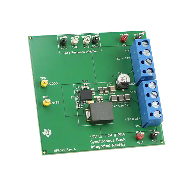
7 Test Point Descriptions........................................................................................................................................................ 10
7.1 Input Voltage Monitoring (TP1 and TP2)..........................................................................................................................10
7.2 Output Voltage Monitoring (TP3 and TP4)....................................................................................................................... 10
7.3 Enable/Soft-start Monitoring (TP5)...................................................................................................................................10
7.4 Power Good Monitoring (TP6)......................................................................................................................................... 10
7.5 Loop Response Testing (TP7, TP8, TP9 and TP10)........................................................................................................10
7.6 Switch Node Voltage Monitoring (TP11 and TP12).......................................................................................................... 10
8 Test Procedures.................................................................................................................................................................... 11
8.1 Start Up/Shut Down Procedure........................................................................................................................................ 11
8.2 Output Ripple Voltage Measurement Procedure.............................................................................................................. 11
8.3 Control Loop Gain and Phase Measurement Procedure................................................................................................. 12
8.4 Equipment Shutdown....................................................................................................................................................... 12
9 Performance Data and Typical Characteristic Curves...................................................................................................... 13
9.1 Efficiency..........................................................................................................................................................................13
9.2 Load Regulation............................................................................................................................................................... 13
9.3 Line Regulation................................................................................................................................................................ 14
9.4 Output Voltage Ripple...................................................................................................................................................... 14
9.5 Switch Node..................................................................................................................................................................... 15
9.6 Load Transient................................................................................................................................................................. 15
9.7 Start Up............................................................................................................................................................................ 16
9.8 Power Off......................................................................................................................................................................... 17
9.9 Over-Current Protection................................................................................................................................................... 17
9.10 Control Loop Bode Plot.................................................................................................................................................. 18
9.11 Thermal Image............................................................................................................................................................... 18
10 EVM Assembly Drawings and PCB Layout...................................................................................................................... 19
11 List of Materials...................................................................................................................................................................22
12 Revision History................................................................................................................................................................. 22
List of Figures
Figure 4-1. TPS56221EVM-579 Schematic.................................................................................................................................6
Figure 5-1. TPS56221EVM-579 Recommended Test Setup....................................................................................................... 8
Figure 8-1. Tip and Barrel Output Voltage Ripple Measurement............................................................................................... 11
Figure 8-2. Control Loop Measurement Setup.......................................................................................................................... 12
Figure 9-1. Efficiency................................................................................................................................................................. 13
Figure 9-2. Load Regulation...................................................................................................................................................... 13
Figure 9-3. Line Regulation (VIN = 8 V to 14 V, VOUT = 1.0 V, IOUT = 25 A).......................................................................... 14
Figure 9-4. Output Voltage Ripple (VIN = 12 V, VOUT = 1.0 V, IOUT = 25 A)...........................................................................14
SLVU446B – MARCH 2011 – REVISED JULY 2021
Submit Document Feedback
TPS56221 Step-Down Converter Evaluation Module User's Guide
Copyright © 2021 Texas Instruments Incorporated
1
�Table of Contents
www.ti.com
Figure 9-5. Switch Node Waveform Measured at Pins Using Tip and Barrel Measurement Technique (VIN = 12 V, VOUT
= 1.0 V, IOUT = 25 A).............................................................................................................................................................15
Figure 9-6. Load Transient (VIN = 12 V, VOUT = 1.0 V, IOUT = 0 A to 25 A)........................................................................... 15
Figure 9-7. Start-Up Waveform (VIN = 12 V, VOUT = 1.0 V, IOUT = 25 A)............................................................................... 16
Figure 9-8. Pre-Biased Start-Up Waveform (VIN = 12 V, VOUT = 1.0 V, IOUT = 0 A).............................................................. 16
Figure 9-9. Power-Off Waveform (VIN = 12 V, VOUT = 1.0 V, IOUT = 25 A)............................................................................ 17
Figure 9-10. Over-Current Protection Waveform (Ch1: VIN, Ch2: EN/SS, Ch3: VOUT, Ch4: IOUT (10 A/div), VIN = 12 V,
VOUT = 1.0 V, IOUT = 36 A)..................................................................................................................................................17
Figure 9-11. Loop Gain (VIN = 12 V, VOUT = 1.0 V, IOUT = 25 A, Bandwidth: 51 kHz, Phase Margin: 48°)............................18
Figure 9-12. Thermal Image (VIN = 14 V, VOUT = 1.0 V, IOUT = 25 A, without airflow)...........................................................18
Figure 10-1. TPS56221EVM-579 Top Assembly Drawing (top view)........................................................................................ 19
Figure 10-2. TPS56221EVM-579 Bottom Assembly Drawing (bottom view).............................................................................19
Figure 10-3. TPS56221EVM-579 Top Copper (top view).......................................................................................................... 20
Figure 10-4. TPS56221EVM-579 Internal 1 (top view)..............................................................................................................20
Figure 10-5. TPS56221EVM-579 Internal 2 (top view)..............................................................................................................21
Figure 10-6. TPS56221EVM-579 Bottom Copper (top view).....................................................................................................21
List of Tables
Table 3-1. TPS56221EVM-579 Electrical Performance Specifications........................................................................................5
Table 7-1. Test Point Descriptions............................................................................................................................................. 10
Table 11-1. TPS56221EVM-579 List of Materials...................................................................................................................... 22
2
TPS56221 Step-Down Converter Evaluation Module User's Guide
Copyright © 2021 Texas Instruments Incorporated
SLVU446B – MARCH 2011 – REVISED JULY 2021
Submit Document Feedback
�www.ti.com
Introduction
1 Introduction
The TPS56221EVM-579 evaluation module (EVM) is a synchronous buck converter providing a fixed 1.0-V
output at up to 25 A from a 12-V input bus. The EVM is designed to start up from a single supply; so, no
additional bias voltage is required for start up. The module uses the TPS56221 High-Current Synchronous Buck
Converter with integrated MOSFETs.
The TPS56221 integrates TI’s high performance controller technology with TI’s industry leading MOSFET
technology in a standard QFN package to meet the demands of modern, high-current, and space constrained
applications.
SLVU446B – MARCH 2011 – REVISED JULY 2021
Submit Document Feedback
TPS56221 Step-Down Converter Evaluation Module User's Guide
Copyright © 2021 Texas Instruments Incorporated
3
�Description
www.ti.com
2 Description
TPS56221EVM-579 is designed to use a regulated 12-V (8-V to 14-V) bus voltage to provide a regulated 1.0-V
output at up to 25 A of load current. TPS56221EVM-579 is designed to demonstrate the TPS56221 high-current
integrated FET converter in a typical space-limited, 12-V bus to low-voltage point-of-load application.
2.1 Applications
•
•
•
•
High-Current, Low-Voltage FPGA or Micro Controller Core Supplies
High-Current Point-of-Load Modules
Telecommunications Equipment
Computer Peripherals
2.2 Features
•
•
•
•
•
•
4
8-V to 14-V Input Voltage Rating
1.0-V ±2% Output Voltage Rating
25-A Steady-State Load Current
500-kHz Switching Frequency
Simple Access to Power Good, Enable/Soft-Start and Error Amplifier
Convenient Converter Performance Test Points
TPS56221 Step-Down Converter Evaluation Module User's Guide
Copyright © 2021 Texas Instruments Incorporated
SLVU446B – MARCH 2011 – REVISED JULY 2021
Submit Document Feedback
�www.ti.com
Electrical Performance Specifications
3 Electrical Performance Specifications
Table 3-1. TPS56221EVM-579 Electrical Performance Specifications
PARAMETER
TEST CONDITIONS
MIN
TYP
MAX
UNIT
Input Characteristics
VIN
Input voltage
IIN
Input current
VIN = 12 V, IOUT = 25 A
No load input current
VIN = 12 V, IOUT = 0 A
43
mA
IOUT = 25 A
4.2
V
VIN_UVLO Input UVLO
8
12
14
V
2.42
A
Output Characteristic
VOUT
VRIPPLE
IOUT
Output voltage
VIN = 8 V to 14 V, IOUT = 0 A to 25 A
Line regulation
VIN = 8 V to 14 V, IOUT = 25 A
0.98
0.1%
1.0
Load regulation
VIN = 12 V, IOUT = 0 A to 25 A
1%
Output voltage ripple
VIN = 12 V, IOUT = 25 A
Output current
VIN = 8 V to 14 V
1.02
20
0
V
mVPP
25
A
550
kHz
Systems Characteristics
fSW
Switching frequency
ηpk
Peak efficiency
VIN = 12 V, IOUT = 13 A
89.6%
Full-load efficiency
VIN = 12 V, IOUT = 25 A
87.1%
η
450
Operating temperature
SLVU446B – MARCH 2011 – REVISED JULY 2021
Submit Document Feedback
500
25
°C
TPS56221 Step-Down Converter Evaluation Module User's Guide
Copyright © 2021 Texas Instruments Incorporated
5
�Schematic
www.ti.com
+
4 Schematic
Figure 4-1. TPS56221EVM-579 Schematic
6
TPS56221 Step-Down Converter Evaluation Module User's Guide
Copyright © 2021 Texas Instruments Incorporated
SLVU446B – MARCH 2011 – REVISED JULY 2021
Submit Document Feedback
�www.ti.com
Test Setup
5 Test Setup
5.1 Test Equipment
5.1.1 Voltage Source
VIN: The input voltage source (VIN) shall be a 0-V to 15-V variable DC source capable of supplying 4 ADC.
5.1.2 Meters
•
•
•
A1: Input current meter (0 ADC to 4 ADC).
V1: Input voltage meter (0 V to 15 V).
V2: Output voltage meter (0 V to 2 V).
5.1.3 Load
LOAD: Output load. Electronic load set for constant current or constant resistance mode, capable of 0 ADC to 25
ADC at 1.0 VDC.
5.1.4 Oscilloscope
For Output Voltage Ripple: Oscilloscope shall be an analog or digital oscilloscope set for AC coupled
measurement with 20-MHz bandwidth limiting. Use 20-mV/div vertical resolution, 1.0-µs/div horizontal resolution.
For Switching Waveforms: Oscilloscope shall be an analog or digital Oscilloscope set for DC coupled
measurement with 20-MHz bandwidth limiting. Use 2-V/div or 5-V/div vertical resolution and 1.0-µs/division
horizontal resolution.
5.1.5 Fan
The TPS56221EVM-579 Evaluation Module includes components that can get hot to touch when operating.
Because this evaluation module is not enclosed to allow probing of circuit nodes, a small fan capable of 200 lfm
to 400 lfm is recommended to reduce component temperatures when operating.
5.2 Recommended Wire Gauge
5.2.1 VIN to J1
The connection between the source voltage (VIN) and J1 of TPS56221EVM-579 can carry as much as 4 ADC of
current. The minimum recommended wire size is AWG #16 with the total length of wire less than 2 feet (1 foot
input, 1 foot return)
5.2.2 J2 to LOAD
The connection between the LOAD and J2 of TPS56221EVM-579 can carry as much as 25 ADC of current. The
minimum recommended wire size is 2xAWG #14 with the total length of wire less than 2 feet (1 foot input, 1 foot
return).
Note
J2 is a 4 position terminal jack using positions for each VOUT and GND. Each position is rated to
support 15 A of output current. When delivering more than 15 A of current, both VOUT and both GND
positions should be used.
SLVU446B – MARCH 2011 – REVISED JULY 2021
Submit Document Feedback
TPS56221 Step-Down Converter Evaluation Module User's Guide
Copyright © 2021 Texas Instruments Incorporated
7
�Test Setup
www.ti.com
5.3 Equipment Set Up Procedure
Figure 5-1 is the recommended test setup to evaluate the TPS56221EVM-579.
FAN
V1
+
+
A1
DC
source
V IN
V2
+
LOAD
1.0V @
25A
+
TEXAS
I NSTRUMENTS
Figure 5-1. TPS56221EVM-579 Recommended Test Setup
1. Working at an ESD workstation, make sure that any wrist straps, bootstraps and mats are connected
referencing the user to earth ground before power is applied to the EVM. Wearing electrostatic smock and
safety glasses is also recommended.
2. Prior to connecting the DC input source, VIN, it is advisable to limit the source current from VIN to 4.0 A
maximum. Make sure VIN is initially set to 0 V and connected as shown in Figure 5-1.
3. Connect VIN to J1 as shown in Figure 5-1.
4. Connect ammeter A1 between VIN and J1 as shown in Figure 5-1.
5. Connect voltmeter V1 to TP1 and TP2 as shown in Figure 5-1.
6. Connect voltmeter V2 to TP3 and TP4 as shown in Figure 5-1.
7. Place the fan as shown in Figure 5-1 and turn it on, ensuring that the air blows directly across the evaluation
module.
8
TPS56221 Step-Down Converter Evaluation Module User's Guide
Copyright © 2021 Texas Instruments Incorporated
SLVU446B – MARCH 2011 – REVISED JULY 2021
Submit Document Feedback
�www.ti.com
Configurations
6 Configurations
6.1 Enable Selection (J3)
The converter can be enabled and disabled by J3. Shorting J3 discharges the soft-start capacitor and disables
the TPS56221 converter. Opening J3 enables the TPS56221 converter.
Default setting: short to disable the converter.
SLVU446B – MARCH 2011 – REVISED JULY 2021
Submit Document Feedback
TPS56221 Step-Down Converter Evaluation Module User's Guide
Copyright © 2021 Texas Instruments Incorporated
9
�Test Point Descriptions
www.ti.com
7 Test Point Descriptions
Table 7-1. Test Point Descriptions
TEST POINT
LABEL
DESCRIPTION
TP1
VIN
Measurement test point for input voltage
TP2
GND
Ground test point for input voltage
TP3
VOUT
Measurement test point for output voltage
TP4
GND
Ground test point for output voltage
TP5
EN/SS
TP6
PGOOD
Measurement test point for enable/soft-start
Measurement test point for power good
TP7
CHA
TP8
SGND
Measurement test point for channel A of loop response
Ground test point for channel A of loop response
TP9
SGND
Ground test point for channel B of loop response
TP10
CHB
Measurement test point for channel B of loop response
TP11
SW
Measurement test point for switch node voltage
TP12
GND
Ground test point for switch node voltage
7.1 Input Voltage Monitoring (TP1 and TP2)
TPS56221EVM-579 provides two test points for measuring the input voltage applied to the module. This allows
the user to measure the actual input module voltage without losses from input cables and connectors. To use
TP1 and TP2, connect a voltmeter positive input terminal to TP1 and negative input terminal to TP2.
7.2 Output Voltage Monitoring (TP3 and TP4)
TPS56221EVM-579 provides two test points for measuring the output voltage generated by the module. To use
TP3 and TP4, connect a voltmeter positive input terminal to TP3 and negative input terminal to TP4. For output
ripple monitoring, please refer to the tip and barrel measurement technique in Section 8.2.
7.3 Enable/Soft-start Monitoring (TP5)
TPS56221EVM-579 provides a test point for measuring the enable/soft-start voltage of the TPS56221 converter.
This test point can be monitored to observe the start-up calibration waveform, soft-start ramp or fault time-out
timing.
The enable/soft-start test point should not be actively driven from an external circuit, such as a logic output of
another power supply.
7.4 Power Good Monitoring (TP6)
TPS56221EVM-579 provides a test points for measuring the Power Good voltage of the TPS56221 converter.
7.5 Loop Response Testing (TP7, TP8, TP9 and TP10)
TPS56221EVM-579 provides four test points (two signals and two grounds) for measuring the control loop
frequency response. This allows the user to measure the actual module loop response without modifying the
evaluation board. See Section 8.3 for additional detail.
7.6 Switch Node Voltage Monitoring (TP11 and TP12)
TPS56221EVM-579 provides two test points for measuring the switch node. To monitor the switch node voltage,
set oscilloscope per Oscilloscope For Switching Waveforms in Section 5.1.4. Connect the oscilloscope probe to
TP11 and the ground lead of the probe to TP12. To monitor the voltage spike on switch node, please remove
the bandwidth limit on the oscilloscope and refer to the Application Report SLPA005 (Reducing Ringing Through
PCB Layout Techniques) for the measurement techniques.
10
TPS56221 Step-Down Converter Evaluation Module User's Guide
Copyright © 2021 Texas Instruments Incorporated
SLVU446B – MARCH 2011 – REVISED JULY 2021
Submit Document Feedback
�www.ti.com
Test Procedures
8 Test Procedures
8.1 Start Up/Shut Down Procedure
1.
2.
3.
4.
5.
6.
7.
8.
9.
10.
11.
Set up the EVM as described in Section 5.3 and Figure 5-1.
Ensure LOAD is set to sink 0 ADC.
Ensure jumper J3 set per Section 6.1.
Increase VIN from 0 VDC to 12 VDC. Using V1 to measure VIN voltage.
Open jumper J3 to enable the converter.
Use V2 to measure VOUT voltage, A1 to measure VIN voltage.
Vary LOAD from 0 ADC to 25 ADC, VOUT should remain in load regulation.
Vary VIN from 8 V to 14 V, VOUT should remain in line regulation.
Short jumper J3 to disable the converter.
Decrease VIN to 0 V.
Decrease LOAD to 0 A.
8.2 Output Ripple Voltage Measurement Procedure
1. Follow Section 8.1 to set VIN and LOAD to desired operating condition.
2. Set oscilloscope for Output Voltage Ripple Measurement in Section 5.1.4.
3. Connect oscilloscope probe with exposed metal barrel to TP3 and TP4 per Figure 8-1. Using a leaded
ground connection may induce additional noise due to the large ground loop.
4. Follow Section 8.1 to power down.
Metal Ground Barrel
Probe Tip
TP3
TP4
Tip and Barrel V OUT ripple
measurement
Figure 8-1. Tip and Barrel Output Voltage Ripple Measurement
SLVU446B – MARCH 2011 – REVISED JULY 2021
Submit Document Feedback
TPS56221 Step-Down Converter Evaluation Module User's Guide
Copyright © 2021 Texas Instruments Incorporated
11
�Test Procedures
www.ti.com
8.3 Control Loop Gain and Phase Measurement Procedure
1.
2.
3.
4.
5.
6.
7.
Follow Section 8.1 to set VIN and LOAD to desired operating condition.
Connect isolation transformer to test points TP7 and TP10 as shown in Figure 8-2.
Connect input signal amplitude measurement probe (Channel A) to TP7 as shown in Figure 8-2.
Connect output signal amplitude measurement probe (Channel B) to TP10 as shown in Figure 8-2.
Connect ground lead of Channel A and Channel B to TP8 and TP9 as shown in Figure 8-2, respectively.
Inject 10 mV or less signal through the isolation transformer.
Sweep the frequency from 500 Hz to 500 kHz with 10-Hz or lower post filter.
æ ChannelB ö
20 ´ log ç
÷
è ChannelA ø .
8. Control loop gain can be measured by
9. Control loop phase can be measured by the phase difference between Channel A and Channel B.
10. Follow Section Section 8.1 to power down.
Network
Analyzer
FAN
CHA CHB Output
V1
+
+
A1
DC
source
VIN
-
Isolation
Transformer
V2
+
LOAD
1.0V @
25A
+
TEXAS
I NSTRUMENTS
Figure 8-2. Control Loop Measurement Setup
8.4 Equipment Shutdown
1.
2.
3.
4.
12
Shut down VIN.
Shut down LOAD.
Shut down fan.
Shut down oscilloscope.
TPS56221 Step-Down Converter Evaluation Module User's Guide
Copyright © 2021 Texas Instruments Incorporated
SLVU446B – MARCH 2011 – REVISED JULY 2021
Submit Document Feedback
�www.ti.com
Performance Data and Typical Characteristic Curves
9 Performance Data and Typical Characteristic Curves
Figure 9-1 through Figure 9-12 present typical performance curves for the TPS56221EVM-579. Since actual
performance data can be affected by measurement techniques and environmental variables, these curves are
presented for reference and may differ from actual field measurements.
9.1 Efficiency
95
90
- Efficiency - %
85
80
75
70
65
VIN = 8 V
60
VIN = 12 V
VIN = 14 V
55
50
0
5
10
15
20
25
ILOAD - Load Current - A
Figure 9-1. Efficiency
9.2 Load Regulation
1.02
VOUT - Output Voltage - V
1.015
1.01
1.005
1
0.995
VIN = 8 V
0.99
VIN = 12 V
0.985
VIN = 14 V
0.98
0
5
10
15
20
25
ILOAD - Load Current - A
Figure 9-2. Load Regulation
SLVU446B – MARCH 2011 – REVISED JULY 2021
Submit Document Feedback
TPS56221 Step-Down Converter Evaluation Module User's Guide
Copyright © 2021 Texas Instruments Incorporated
13
�Performance Data and Typical Characteristic Curves
www.ti.com
9.3 Line Regulation
1.02
VOUT - Output Voltage - V
1.015
1.01
1.005
1
0.995
0.99
0.985
0.98
8
9
10
11
12
13
14
VIN - Input Voltage - V
Figure 9-3. Line Regulation (VIN = 8 V to 14 V, VOUT = 1.0 V, IOUT = 25 A)
9.4 Output Voltage Ripple
Figure 9-4. Output Voltage Ripple (VIN = 12 V, VOUT = 1.0 V, IOUT = 25 A)
14
TPS56221 Step-Down Converter Evaluation Module User's Guide
Copyright © 2021 Texas Instruments Incorporated
SLVU446B – MARCH 2011 – REVISED JULY 2021
Submit Document Feedback
�www.ti.com
Performance Data and Typical Characteristic Curves
9.5 Switch Node
Figure 9-5. Switch Node Waveform Measured at Pins Using Tip and Barrel Measurement Technique (VIN
= 12 V, VOUT = 1.0 V, IOUT = 25 A)
9.6 Load Transient
Figure 9-6. Load Transient (VIN = 12 V, VOUT = 1.0 V, IOUT = 0 A to 25 A)
SLVU446B – MARCH 2011 – REVISED JULY 2021
Submit Document Feedback
TPS56221 Step-Down Converter Evaluation Module User's Guide
Copyright © 2021 Texas Instruments Incorporated
15
�Performance Data and Typical Characteristic Curves
www.ti.com
9.7 Start Up
Figure 9-7. Start-Up Waveform (VIN = 12 V, VOUT = 1.0 V, IOUT = 25 A)
Figure 9-8. Pre-Biased Start-Up Waveform (VIN = 12 V, VOUT = 1.0 V, IOUT = 0 A)
16
TPS56221 Step-Down Converter Evaluation Module User's Guide
Copyright © 2021 Texas Instruments Incorporated
SLVU446B – MARCH 2011 – REVISED JULY 2021
Submit Document Feedback
�www.ti.com
Performance Data and Typical Characteristic Curves
9.8 Power Off
Figure 9-9. Power-Off Waveform (VIN = 12 V, VOUT = 1.0 V, IOUT = 25 A)
9.9 Over-Current Protection
Figure 9-10. Over-Current Protection Waveform (Ch1: VIN, Ch2: EN/SS, Ch3: VOUT, Ch4: IOUT (10 A/div),
VIN = 12 V, VOUT = 1.0 V, IOUT = 36 A)
SLVU446B – MARCH 2011 – REVISED JULY 2021
Submit Document Feedback
TPS56221 Step-Down Converter Evaluation Module User's Guide
Copyright © 2021 Texas Instruments Incorporated
17
�Performance Data and Typical Characteristic Curves
www.ti.com
9.10 Control Loop Bode Plot
Figure 9-11. Loop Gain (VIN = 12 V, VOUT = 1.0 V, IOUT = 25 A, Bandwidth: 51 kHz, Phase Margin: 48°)
9.11 Thermal Image
Figure 9-12. Thermal Image (VIN = 14 V, VOUT = 1.0 V, IOUT = 25 A, without airflow)
18
TPS56221 Step-Down Converter Evaluation Module User's Guide
Copyright © 2021 Texas Instruments Incorporated
SLVU446B – MARCH 2011 – REVISED JULY 2021
Submit Document Feedback
�www.ti.com
EVM Assembly Drawings and PCB Layout
10 EVM Assembly Drawings and PCB Layout
The following figures (Figure 10-1 through Figure 10-6) show the design of the TPS56221EVM-579 printed
circuit board. The EVM has been designed using a 4-layer, 2-oz copper-clad circuit board 2.5” x 2.5” with
components on both sides of the PCB to allow the user to view, probe and evaluate the TPS56221 high current
converter with integrated FETs in a small form factor, high-current application.
TEXAS
I NSTRUMENTS
Figure 10-1. TPS56221EVM-579 Top Assembly Drawing (top view)
Figure 10-2. TPS56221EVM-579 Bottom Assembly Drawing (bottom view)
SLVU446B – MARCH 2011 – REVISED JULY 2021
Submit Document Feedback
TPS56221 Step-Down Converter Evaluation Module User's Guide
Copyright © 2021 Texas Instruments Incorporated
19
�EVM Assembly Drawings and PCB Layout
www.ti.com
Figure 10-3. TPS56221EVM-579 Top Copper (top view)
Figure 10-4. TPS56221EVM-579 Internal 1 (top view)
20
TPS56221 Step-Down Converter Evaluation Module User's Guide
Copyright © 2021 Texas Instruments Incorporated
SLVU446B – MARCH 2011 – REVISED JULY 2021
Submit Document Feedback
�www.ti.com
EVM Assembly Drawings and PCB Layout
Figure 10-5. TPS56221EVM-579 Internal 2 (top view)
Figure 10-6. TPS56221EVM-579 Bottom Copper (top view)
SLVU446B – MARCH 2011 – REVISED JULY 2021
Submit Document Feedback
TPS56221 Step-Down Converter Evaluation Module User's Guide
Copyright © 2021 Texas Instruments Incorporated
21
�List of Materials
www.ti.com
11 List of Materials
Table 11-1. TPS56221EVM-579 List of Materials
QTY
REF DES
DESCRIPTION
PART NUMBER
MFR
4
C1, C2, C3, C4
Capacitor, ceramic, 25 V, X5R, 20%, 22 µF, 1210
Std
Std
2
C5, C11
Capacitor, ceramic, 25 V, X5R, 20%, 1.0 µF, 0805
Std
Std
0
C6
Capacitor, aluminum, 16 VDC, ±20%, 100 µF, code D8
EEEFP1C101AP
Panasonic
5
C7, C8, C9,
C10, C19
Capacitor, ceramic, 6.3 V, X5R, 20%, 100 µF, 1210
Std
Std
1
C12
Capacitor, ceramic, 10 V, X5R, 20%, 4.7 µF, 0805
Std
Std
1
C13
Capacitor, ceramic, 16 V, X7R, 20%, 33 nF, 0603
Std
Std
1
C14
Capacitor, ceramic, 50 V, X7R, 20%, 100 nF, 0603
Std
Std
2
C15, C18
Capacitor, ceramic, 50 V, X7R, 10%, 2200 pF, 0603
Std
Std
1
C16
Capacitor, ceramic, 50 V, C0G, 5%, 100 pF, 0603
Std
Std
1
C17
Capacitor, ceramic, 50 V, C0G, 5%, 680 pF, 0603
Std
Std
0
C20, C21
Capacitor, ceramic, 6.3 V, X5R, 20%, 100 µF, 1210
Std
Std
2
J1, J2
Terminal block, 4 pin, 15 A, 5.1 mm, 0.80 inch x 0.35 inch
ED120/4DS
OST
1
J3
Header, male 2 pin, 100-mil spacing, 0.100 inch x 2 inch
PEC02SAAN
Sullins
1
L1
Inductor, 0.32 mΩ, 320 nH, 0.530 inch x 0.510 inch
PA0513.321NLT
Pulse
1
R1
Resistor, chip, 1/16 W, 1%, 2.87 kΩ, 0603
Std
Std
1
R2
Resistor, chip, 1/16 W, 1%, 5.10 Ω, 0603
Std
Std
1
R3
Resistor, chip, 1/16 W, 1%, 7.87 kΩ, 0603
Std
Std
1
R4
Resistor, chip, 1/16 W, 1%, 20.5 kΩ, 0603
Std
Std
1
R5
Resistor, chip, 1/16 W, 1%, 49.9 Ω, 0603
Std
Std
1
R6
Resistor, chip, 1/16 W, 1%, 1.00 kΩ, 0603
Std
Std
1
R7
Resistor, chip, 1/16 W, 1%, 30.1 kΩ, 0603
Std
Std
1
R8
Resistor, chip, 1/16 W, 1%, 0 kΩ, 0603
Std
Std
1
R9
Resistor, chip, 1/8 W, 1%, 1.00 Ω, 0805
Std
Std
1
R10
Resistor, chip, 1/16 W, 1%, 100 kΩ, 0603
Std
Std
3
TP1, TP3, TP11
Test point, red, thru hole, 0.125 inch x 0.125 inch
5010
Keystone
5
TP2, TP4, TP8,
TP9, TP12
Test point, black, thru hole, 0.125 inch x 0.125 inch
5011
Keystone
2
TP5, TP6
Test point, yellow, thru hole, 0.125 x 0.125 inch
5014
Keystone
2
TP7, TP10
Test point, white, thru hole, 0.125 x 0.125 inch
5012
Keystone
1
U1
4.5-V to 14-V Input 25-A Synchronous Buck Converter,
QFN-22 6 mm x 5 mm
TPS56221DQP
TI
1
--
PCB, 2.5 inch x 2.5 inch x 0.062 inch
HPA579
Any
1
--
Shunt, 100 mil, black, 0.100
929950-00
3M
12 Revision History
NOTE: Page numbers for previous revisions may differ from page numbers in the current version.
Changes from Revision A (March 2011) to Revision B (July 2021)
Page
• Updated user's guide title................................................................................................................................... 3
• Updated the numbering format for tables, figures, and cross-references throughout the document. ................3
22
TPS56221 Step-Down Converter Evaluation Module User's Guide
Copyright © 2021 Texas Instruments Incorporated
SLVU446B – MARCH 2011 – REVISED JULY 2021
Submit Document Feedback
�IMPORTANT NOTICE AND DISCLAIMER
TI PROVIDES TECHNICAL AND RELIABILITY DATA (INCLUDING DATA SHEETS), DESIGN RESOURCES (INCLUDING REFERENCE
DESIGNS), APPLICATION OR OTHER DESIGN ADVICE, WEB TOOLS, SAFETY INFORMATION, AND OTHER RESOURCES “AS IS”
AND WITH ALL FAULTS, AND DISCLAIMS ALL WARRANTIES, EXPRESS AND IMPLIED, INCLUDING WITHOUT LIMITATION ANY
IMPLIED WARRANTIES OF MERCHANTABILITY, FITNESS FOR A PARTICULAR PURPOSE OR NON-INFRINGEMENT OF THIRD
PARTY INTELLECTUAL PROPERTY RIGHTS.
These resources are intended for skilled developers designing with TI products. You are solely responsible for (1) selecting the appropriate
TI products for your application, (2) designing, validating and testing your application, and (3) ensuring your application meets applicable
standards, and any other safety, security, regulatory or other requirements.
These resources are subject to change without notice. TI grants you permission to use these resources only for development of an
application that uses the TI products described in the resource. Other reproduction and display of these resources is prohibited. No license
is granted to any other TI intellectual property right or to any third party intellectual property right. TI disclaims responsibility for, and you
will fully indemnify TI and its representatives against, any claims, damages, costs, losses, and liabilities arising out of your use of these
resources.
TI’s products are provided subject to TI’s Terms of Sale or other applicable terms available either on ti.com or provided in conjunction with
such TI products. TI’s provision of these resources does not expand or otherwise alter TI’s applicable warranties or warranty disclaimers for
TI products.
TI objects to and rejects any additional or different terms you may have proposed. IMPORTANT NOTICE
Mailing Address: Texas Instruments, Post Office Box 655303, Dallas, Texas 75265
Copyright © 2022, Texas Instruments Incorporated
�