www.ti.com
Table of Contents
User’s Guide
TPS56C215 SWIFT™ Buck Converter Evaluation Module
User's Guide
ABSTRACT
This user’s guide contains information for the TPS56C215EVM-762 evaluation module (PWR762) as well as for
the TPS56C215 dc/dc converter. Also included are the performance specifications, the schematic, and the bill of
materials for the TPS56C215EVM-762.
Table of Contents
1 Introduction.............................................................................................................................................................................2
2 Test Setup and Results.......................................................................................................................................................... 3
3 Board Layout.........................................................................................................................................................................13
4 Schematic and Bill of Materials...........................................................................................................................................16
5 Revision History................................................................................................................................................................... 18
List of Figures
Figure 2-1. TPS56C215EVM-762 Efficiency................................................................................................................................4
Figure 2-2. TPS56C215EVM-762 Low Current Efficiency........................................................................................................... 4
Figure 2-3. TPS56C215EVM-762 Load Regulation, VIN = 5 V.................................................................................................... 5
Figure 2-4. TPS56C215EVM-762 Load Regulation, VIN = 12 V.................................................................................................. 5
Figure 2-5. TPS56C215EVM-762 Line Regulation......................................................................................................................6
Figure 2-6. TPS56C215EVM-762 Transient Response...............................................................................................................6
Figure 2-7. TPS56C215EVM-762 Loop Response......................................................................................................................7
Figure 2-8. TPS56C215EVM-762 Output Ripple, 10 mA Load................................................................................................... 7
Figure 2-9. TPS56C215EVM-762 Output Ripple, 800 mA Load................................................................................................. 8
Figure 2-10. TPS56C215EVM-762 Output Ripple, 12-A Load.................................................................................................... 8
Figure 2-11. TPS56C215EVM-762 Input Ripple, 10-mA Load.................................................................................................... 9
Figure 2-12. TPS56C215EVM-762 Input Ripple, 800-mA Load.................................................................................................. 9
Figure 2-13. TPS56C215EVM-762 Input Ripple, 12-A Load..................................................................................................... 10
Figure 2-14. TPS56C215EVM-762 Start-Up Relative to VIN .....................................................................................................11
Figure 2-15. TPS56C215EVM-762 Start-Up Relative to Enable................................................................................................11
Figure 2-16. Shutdown Relative to VIN ..................................................................................................................................... 12
Figure 2-17. Shutdown Relative to Enable................................................................................................................................ 12
Figure 3-1. TPS56C215EVM-762 Top-Side Assembly.............................................................................................................. 13
Figure 3-2. TPS56C215EVM-762 Top-Side Layout...................................................................................................................14
Figure 3-3. TPS56C215EVM-762 Internal Layer-1 Layout........................................................................................................14
Figure 3-4. TPS56C215EVM-762 Internal Layer-2 Layout........................................................................................................15
Figure 3-5. TPS56C215EVM-762 Bottom-Side Layout............................................................................................................. 15
Figure 4-1. TPS56C215EVM-762 Schematic............................................................................................................................ 16
List of Tables
Table 1-1. Input Voltage and Output Current Summary...............................................................................................................2
Table 1-2. TPS56C215EVM-762 Performance Specification Summary...................................................................................... 2
Table 2-1. EVM Connectors and Test Points............................................................................................................................... 3
Table 4-1. TPS56C215EVM-762 Bill of Materials...................................................................................................................... 17
Trademarks
All trademarks are the property of their respective owners.
SLVUAO9C – MARCH 2016 – REVISED JUNE 2021
Submit Document Feedback
TPS56C215 SWIFT™ Buck Converter Evaluation Module User's Guide
Copyright © 2021 Texas Instruments Incorporated
1
�Introduction
www.ti.com
1 Introduction
1.1 Background
The TPS56C215 dc/dc converter is a synchronous buck converter designed to provide up to a 14-A output.
The input (VIN) is rated for 4.5 V to 17 V. The TPS56C215 uses a proprietary DCAP3 Control mode and a
MODE pin is used to select output current limit, switching frequency, and Forced Continuous Conduction Mode
(FCCM)/Discontinuous Conduction Mode (DCM) operation. Rated input voltage and output current range for
the evaluation module are given in Table 1-1. This evaluation module is designed to demonstrate the small
printed-circuit-board areas that may be achieved when designing with the TPS56C215 regulator. The MODE pin
is configured for 1.2-MHz switching frequency, 12-A and DCM operation. The high-side and low-side MOSFETs
are incorporated inside the TPS56C215 package along with the gate drive circuitry. The low drain-to-source
on-resistance of the MOSFET allows the TPS56C215 to achieve high efficiencies and helps keep the junction
temperature low at high output currents. An external divider allows for an adjustable output voltage. Additionally,
the TPS56C215 provides adjustable slow start and undervoltage lockout inputs and a power good output.
Table 1-1. Input Voltage and Output Current Summary
EVM
Input Voltage Range
Output Current Range
TPS56C215EVM-762
VIN = 4.5 V to 17 V
0 A to 12 A
1.2 Performance Specification Summary
A summary of the TPS56C215EVM-762 performance specifications is provided in Table 1-2. Specifications
are given for an input voltage of VIN = 12 V and an output voltage of 1.2 V, unless otherwise specified. The
TPS56C215EVM-762 is designed and tested for VIN = 4.5 V to 17 V. The ambient temperature is 25°C for all
measurements, unless otherwise noted.
Table 1-2. TPS56C215EVM-762 Performance Specification Summary
Specification
Test Conditions
VIN voltage range
MIN
4.5
TYP
MAX
12
17
Unit
V
VIN start voltage
Internal
UVLO
V
VIN stop voltage
Internal
UVLO
V
Output voltage setpoint
1.2
Output current range
VIN = 9.2 V to 14 V
Line regulation
IO = 6 A, VIN = 4.5 V to 17 V
±0.05%
VIN = 12 V, IO = 0 A to 12 A
–0.02%,
+0.6%
Load regulation
IO = 3 A to 9 A
Load transient response
IO = 9 A to 3 A
0
V
12
A
Voltage change
–30
Recovery time
50
µs
Voltage change
30
mV
Recovery time
mV
50
µs
135
kHz
72
degree
120
mVPP
Loop bandwidth
VIN = 12 V, IO = 6 A
Phase margin
VIN = 12 V , IO = 6 A
Input ripple voltage
IO = 12 A
Output ripple voltage
IO = 12 A
10
mVPP
6
ms
Output rise time
Operating frequency
Maximum efficiency
1.2
TPS56C215EVM-762, VIN = 5 V, IO = 5.7 A
MHz
82.2%
1.3 Modifications
These evaluation modules are designed to provide access to the features of the TPS56C215. Some
modifications can be made to this module.
2
TPS56C215 SWIFT™ Buck Converter Evaluation Module User's Guide
Copyright © 2021 Texas Instruments Incorporated
SLVUAO9C – MARCH 2016 – REVISED JUNE 2021
Submit Document Feedback
�www.ti.com
Introduction
1.3.1 Output Voltage Setpoint
The output voltage is set by the resistor divider network of R7 (R(TOP)) and R9 (R(BOT)). R9 is fixed at 10.0 kΩ. To
change the output voltage of the EVM, it is necessary to change the value of resistor R7. Changing the value of
R9 can change the output voltage above the 0.6 V reference voltage VREF. The value of R7 for a specific output
voltage can be calculated using Equation 1.
R (TOP) =
R (BOT) x (VOUT - VREF )
VREF
(1)
1.3.2 Adjustable UVLO
The undervoltage lockout (UVLO) can be adjusted externally using R1 (REN(TOP)) and R2 (REN(BOT)). R1 and R2
are not populated on the EVM, which uses the internal UVLO default settings. See the TPS56C215 datasheet
(SLVSD05) for detailed instructions for setting the external UVLO.
2 Test Setup and Results
This section describes how to properly connect, set up, and use the TPS56C215EVM-762 evaluation module.
The section also includes test results typical for the evaluation module and covers efficiency, output voltage
regulation, load transients, loop response, output ripple, input ripple, and start-up.
2.1 Input/Output Connections
The TPS56C215EVM-762 is provided with input/output connectors and test points as shown in Table 2-1. A
power supply capable of supplying greater than 4 A must be connected to J1 through a pair of 20-AWG wires or
better. The load must be connected to J2 through a pair of 20-AWG wires or better. The maximum load current
capability is 12 A. Wire lengths must be minimized to reduce losses in the wires. Test-point TP1 provides a place
to monitor the VIN input voltages with TP2 providing a convenient ground reference. TP9 is used to monitor the
output voltage with TP10 as the ground reference.
Table 2-1. EVM Connectors and Test Points
Reference Designator
Function
J1
VIN input voltage connector. (See Table 1-1 for VIN range)
J2
1.2 V at 10 A maximum
J3
2-pin header for enable. Connect EN to ground to disable, open to enable. VOUT.
J4
VOUT, 1.2 V at 10 A maximum
TP1
VIN test point
TP2
GND test point at VIN connector
TP3
Slow Start (SS) test point
TP4
PGOOD test point
TP5
VREG5 test point
TP6
Test point between voltage divider network and output. Used for loop response measurements
TP7
SW node test point
TP8
AGND test point
TP9
VOUT test point
TP10
GND test point
SLVUAO9C – MARCH 2016 – REVISED JUNE 2021
Submit Document Feedback
TPS56C215 SWIFT™ Buck Converter Evaluation Module User's Guide
Copyright © 2021 Texas Instruments Incorporated
3
�Test Setup and Results
www.ti.com
2.2 Efficiency
The efficiency of this EVM peaks at a load current of about 5 A and then decreases as the load current increases
toward full load. Figure 2-1 shows the efficiency for the TPS56C215EVM-762 at an ambient temperature of
25°C.
100
90
80
Efficiency (%)
70
60
50
40
30
20
10
VIN = 5V
VIN = 12V
0
0
1
2
3
4
5
6
7
Output Current (A)
8
9
10
11
12
D001
Figure 2-1. TPS56C215EVM-762 Efficiency
Figure 2-2 shows the efficiency for the TPS56C215EVM-762 using a semi-log scale to more easily show
efficiency at lower output currents. The ambient temperature is 25°C.
100
90
80
Efficiency (%)
70
60
50
40
30
20
10
0
0.001
VIN = 5V
VIN = 12V
0.0020.003 0.005
0.01
0.02 0.03
0.05 0.07 0.1
0.2
Output Current (A)
0.3 0.40.5 0.7
1
2
3
4 5 6 7 8 1012
D002
Figure 2-2. TPS56C215EVM-762 Low Current Efficiency
The efficiency may be lower at higher ambient temperatures, due to temperature variation in the drain-to-source
resistance of the internal MOSFET.
4
TPS56C215 SWIFT™ Buck Converter Evaluation Module User's Guide
Copyright © 2021 Texas Instruments Incorporated
SLVUAO9C – MARCH 2016 – REVISED JUNE 2021
Submit Document Feedback
�www.ti.com
Test Setup and Results
2.3 Output Voltage Load Regulation
Figure 2-3 and Figure 2-4 show the load regulation for the TPS56C215EVM-762.
1
0.8
0.6
Load Regulation (%)
0.4
0.2
0
-0.2
-0.4
-0.6
-0.8
-1
0
1
2
3
4
5
6
7
Output Current (A)
8
9
10
11
12
D003
Figure 2-3. TPS56C215EVM-762 Load Regulation, VIN = 5 V
1
0.8
0.6
Load Regulation (%)
0.4
0.2
0
-0.2
-0.4
-0.6
-0.8
-1
0
1
2
3
4
5
6
7
Output Current (A)
8
9
10
11
12
D003
Figure 2-4. TPS56C215EVM-762 Load Regulation, VIN = 12 V
Measurements are given for an ambient temperature of 25°C.
SLVUAO9C – MARCH 2016 – REVISED JUNE 2021
Submit Document Feedback
TPS56C215 SWIFT™ Buck Converter Evaluation Module User's Guide
Copyright © 2021 Texas Instruments Incorporated
5
�Test Setup and Results
www.ti.com
2.4 Output Voltage Line Regulation
Figure 2-5 shows the line regulation for the TPS56C215EVM-762.
0.25
0.20
0.15
Line Regulation (%)
0.10
0.05
0.00
-0.05
-0.10
-0.15
-0.20
-0.25
4
5
6
7
8
9
10
11
12
Input Voltage (V)
13
14
15
16
17
18
D005
Figure 2-5. TPS56C215EVM-762 Line Regulation
2.5 Load Transients
Figure 2-6 shows the TPS56C215EVM-762 response to load transients. The current step is from 3 A to 9 A. The
current step slew rate is 1 A/µs. Total peak-to-peak voltage variation is as shown, including ripple and noise on
the output. The transient waveform is measured using the on-board fast transient circuit.
VO = 50 mV / div (ac coupled)
IO = 2 A / div
Load step = 3 A - 9 A, slew rate = 1 A / µsec
Time = 200 µsec / div
Figure 2-6. TPS56C215EVM-762 Transient Response
6
TPS56C215 SWIFT™ Buck Converter Evaluation Module User's Guide
Copyright © 2021 Texas Instruments Incorporated
SLVUAO9C – MARCH 2016 – REVISED JUNE 2021
Submit Document Feedback
�www.ti.com
Test Setup and Results
2.6 Loop Characteristics
60
180
50
150
40
120
30
90
20
60
10
30
0
0
-10
-30
-20
-60
-30
-90
-40
-120
-50
Gain (dB)
-150
Phase (Deg)
-180
200000
500000
-60
100
200
300
500 700 1000
2000 3000
5000
10000
Frequency (Hz)
2000030000 50000
100000
Phase (Degree)
Gain (dB)
Figure 2-7 shows the TPS56C215EVM-762 loop-response characteristics. Gain and phase plots are shown for
VIN voltage of 12 V. Load current for the measurement is 5 A.
D006
Figure 2-7. TPS56C215EVM-762 Loop Response
2.7 Output Voltage Ripple
Figure 2-8, Figure 2-9, and Figure 2-10 show the TPS56C215EVM-762 output voltage ripple. The load currents
are 10 mA, 800 mA and 12 A. VIN = 12 V. The ripple voltage is measured directly across TP7 and TP8.
VOUT = 20 mV / div (ac coupled)
SW = 5 V / div
Time = 50 µsec / div
Figure 2-8. TPS56C215EVM-762 Output Ripple, 10 mA Load
SLVUAO9C – MARCH 2016 – REVISED JUNE 2021
Submit Document Feedback
TPS56C215 SWIFT™ Buck Converter Evaluation Module User's Guide
Copyright © 2021 Texas Instruments Incorporated
7
�Test Setup and Results
www.ti.com
VOUT = 20 mV / div (ac coupled)
SW = 5 V / div
Time = 500 nsec / div
Figure 2-9. TPS56C215EVM-762 Output Ripple, 800 mA Load
VOUT = 20 mV / div (ac coupled)
SW = 5 V / div
Time = 500 nsec / div
Figure 2-10. TPS56C215EVM-762 Output Ripple, 12-A Load
8
TPS56C215 SWIFT™ Buck Converter Evaluation Module User's Guide
Copyright © 2021 Texas Instruments Incorporated
SLVUAO9C – MARCH 2016 – REVISED JUNE 2021
Submit Document Feedback
�www.ti.com
Test Setup and Results
2.8 Input Voltage Ripple
Figure 2-11, Figure 2-12, and Figure 2-13 show the TPS56C215EVM-762 input voltage ripple. The load currents
are 10 mA, 800 mA and 12 A. VIN = 12 V. The ripple voltage is measured directly across TP1 and TP2.
VIN = 100 mV / div (ac coupled)
SW = 5 V / div
Time = 50 µsec / div
Figure 2-11. TPS56C215EVM-762 Input Ripple, 10-mA Load
VIN = 100 mV / div (ac coupled)
SW = 5 V / div
Time = 500 nsec / div
Figure 2-12. TPS56C215EVM-762 Input Ripple, 800-mA Load
SLVUAO9C – MARCH 2016 – REVISED JUNE 2021
Submit Document Feedback
TPS56C215 SWIFT™ Buck Converter Evaluation Module User's Guide
Copyright © 2021 Texas Instruments Incorporated
9
�Test Setup and Results
www.ti.com
VIN = 100 mV / div (ac coupled)
SW = 5 V / div
Time = 500 nsec / div
Figure 2-13. TPS56C215EVM-762 Input Ripple, 12-A Load
10
TPS56C215 SWIFT™ Buck Converter Evaluation Module User's Guide
Copyright © 2021 Texas Instruments Incorporated
SLVUAO9C – MARCH 2016 – REVISED JUNE 2021
Submit Document Feedback
�www.ti.com
Test Setup and Results
2.9 Powering Up
Figure 2-14 and Figure 2-15 show the start-up waveforms for the TPS56C215EVM-762. In Figure 2-14, the
output voltage ramps up as soon as the input voltage reaches the UVLO threshold. In Figure 2-15, the input
voltage is initially applied and the output is inhibited by using a jumper at J2 to tie EN to GND. When the jumper
is removed, EN is released. When the EN voltage reaches the enable-threshold voltage, the start-up sequence
begins and the output voltage ramps up to the externally set value of 1.2 V. The input voltage for these plots is
12 V and the load is 1 Ω.
VIN = 10 V / div
EN = 5 V / div
VO = 500 mV / div
PG = 5 V / div
Time = 2 msec / div
Figure 2-14. TPS56C215EVM-762 Start-Up Relative to VIN
VIN = 10 V / div
EN = 5 V / div
VO = 500 mV / div
PG = 5 V / div
Time = 2 msec / div
Figure 2-15. TPS56C215EVM-762 Start-Up Relative to Enable
SLVUAO9C – MARCH 2016 – REVISED JUNE 2021
Submit Document Feedback
TPS56C215 SWIFT™ Buck Converter Evaluation Module User's Guide
Copyright © 2021 Texas Instruments Incorporated
11
�Test Setup and Results
www.ti.com
2.10 Powering Down
Figure 2-16 and Figure 2-17 show the shutdown waveforms for the TPS56C215EVM-762. The input voltage for
these plots is 12 V and the load is 1 Ω.
VIN = 10 V / div
EN = 5 V / div
VO = 500 mV / div
PG = 5 V / div
Time = 2 msec / div
Figure 2-16. Shutdown Relative to VIN
VIN = 10 V / div
EN = 5 V / div
VO = 500 mV / div
PG = 5 V / div
Time = 2 msec / div
Figure 2-17. Shutdown Relative to Enable
12
TPS56C215 SWIFT™ Buck Converter Evaluation Module User's Guide
Copyright © 2021 Texas Instruments Incorporated
SLVUAO9C – MARCH 2016 – REVISED JUNE 2021
Submit Document Feedback
�www.ti.com
Board Layout
3 Board Layout
This section provides a description of the TPS56C215EVM-762 board layout and layer illustrations.
3.1 Layout
The board layout for the TPS56C215EVM-762 is shown in Figure 3-1 through Figure 3-5. The top-side layer of
the EVM is laid out in a manner typical of a user application. The top, bottom, and internal layers are
2-oz. copper.
The top layer contains the main power traces for VIN, VOUT, and SW. Also on the top layer are connections
for the remaining pins of the TPS56C215 and the majority of the signal traces. There is a large area filled with
ground. The internal layer-1 is dedicated ground plane with an island for quiet analog ground that is connected
to the main power ground plane at a single point. The internal layer-2 contains an additional large ground copper
area as well as an additional VIN and VOUT copper fill. The bottom layer is another ground plane with two
additional traces for the output voltage feedback and BST capacitor connection. The top-side ground traces are
connected to the bottom and internal ground planes with multiple vias placed around the board.
The input decoupling capacitors and bootstrap capacitor are all located as close to the IC as possible.
Additionally, the voltage setpoint resistor divider components are kept close to the IC. The voltage divider
network ties to the output voltage at the point of regulation, the copper VOUT trace at the TP9 test point. For the
TPS56C215, an additional input bulk capacitor may be required, depending on the EVM connection to the input
supply. Critical analog circuits such as the voltage set point divider, EN resistor, SS capacitor, MODE resistor,
and AGND pin are terminated to quiet analog ground island on the internal layer-1.
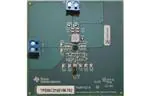
Figure 3-1. TPS56C215EVM-762 Top-Side Assembly
SLVUAO9C – MARCH 2016 – REVISED JUNE 2021
Submit Document Feedback
TPS56C215 SWIFT™ Buck Converter Evaluation Module User's Guide
Copyright © 2021 Texas Instruments Incorporated
13
�Board Layout
www.ti.com
Figure 3-2. TPS56C215EVM-762 Top-Side Layout
Figure 3-3. TPS56C215EVM-762 Internal Layer-1 Layout
14
TPS56C215 SWIFT™ Buck Converter Evaluation Module User's Guide
Copyright © 2021 Texas Instruments Incorporated
SLVUAO9C – MARCH 2016 – REVISED JUNE 2021
Submit Document Feedback
�www.ti.com
Board Layout
Figure 3-4. TPS56C215EVM-762 Internal Layer-2 Layout
Figure 3-5. TPS56C215EVM-762 Bottom-Side Layout
SLVUAO9C – MARCH 2016 – REVISED JUNE 2021
Submit Document Feedback
TPS56C215 SWIFT™ Buck Converter Evaluation Module User's Guide
Copyright © 2021 Texas Instruments Incorporated
15
�Schematic and Bill of Materials
www.ti.com
4 Schematic and Bill of Materials
This section presents the TPS56C215EVM-762 schematic and bill of materials.
4.1 Schematic
Figure 4-1 is the schematic for the TPS56C215EVM-762.
VIN = 4.5 V - 17 V
TP1
C1
0.1µF
J1
C2
0.1µF
C3
22µF
C4
22µF
C5
22µF
TP2
R1
DNP
57.6k
C7
0.047µF
R3
TP4
10.0k
R4
R2
DNP
12.1k
14
15
V5
V5
52.3k
R5
49.9k
TPS56C215RNN
16
18
VIN
VIN
SW
SW
FB
SS
EN
PGOOD
MODE
TP5
17
BOOT
PGND
PGND
PGND
PGND
PGND
PGND
VREG5
AGND
C8
4.7µF
TP7
1
6
7
13
3
4
5
8
9
10
VOUT = 1.2 V, 12 A
L1
C9
2
11
TP3
J3
U1
C6
22µF
TP9
470nH
0.1µF
R8
R7 TP8
10.0k
C10
0
R6
0
C11
47µF
C12
47µF
C13
47µF
C14
47µF
TP10
J2
56pF
R9
10.0k
12
TP6
Copyright © 2017, Texas Instruments Incorporated
Figure 4-1. TPS56C215EVM-762 Schematic
16
TPS56C215 SWIFT™ Buck Converter Evaluation Module User's Guide
Copyright © 2021 Texas Instruments Incorporated
SLVUAO9C – MARCH 2016 – REVISED JUNE 2021
Submit Document Feedback
�www.ti.com
Schematic and Bill of Materials
4.2 Bill of Materials
Table 4-1 presents the bill of materials for the TPS56C215EVM-762.
Table 4-1. TPS56C215EVM-762 Bill of Materials
Designator
Qty
Value
Description
!PCB1
1
Package Reference
Part Number
Manufacturer
PWR762
C1, C2, C9
3
0.1uF
CAP, CERM, 0.1 µF, 25 V, +/- 10%, X7R, 0603
Any
0603
GRM188R71E104KA01D
Murata
C3, C4, C5, C6
4
22uF
C7
1
0.047uF
CAP, CERM, 22 µF, 35 V, +/- 20%, X5R, 0805
0805
C2012X5R1V226M125AC
TDK
CAP, CERM, 0.047 µF, 50 V, +/- 10%, X7R, 0603
0603
GRM188R71H473KA61D
C8
1
Murata
4.7uF
CAP, CERM, 4.7 µF, 10 V, +/- 20%, X5R, 0603
0603
GRM188R61A475ME15
C10
Murata
1
56pF
CAP, CERM, 56 pF, 50 V, +/- 5%, C0G/NP0, 0603
0603
GRM1885C1H560JA01D
Murata
C11, C12, C13, C14
4
47uF
CAP, CERM, 47 µF, 10 V, +/- 20%, X5R, 0805
0805
GRM21BR61A476ME15
Murata
J1, J2
2
TERMINAL BLOCK 5.08MM VERT 2POS, TH
ED120/2DS
On-Shore Technology
J3
1
Header, 100mil, 2x1, Gold, TH
HTSW-102-07-G-S
Samtec
L1
1
LBL1
1
R3, R7, R9
3
R4
1
R5
Printed Circuit Board
Inductor, Shielded Drum Core, Powdered Iron, 470 nH, 17.5 A,
0.004 ohm, SMD
IHLP-2525CZ
IHLP2525CZERR47M01
Vishay-Dale
Thermal Transfer Printable Labels, 1.250" W x 0.250" H - 10,000
per roll
PCB Label 1.25"H x 0.250"W
THT-13-457-10
Brady
10.0k
RES, 10.0 k, 1%, 0.1 W, 0603
0603
CRCW060310K0FKEA
Vishay-Dale
52.3k
RES, 52.3 k, 1%, 0.1 W, 0603
0603
CRCW060352K3FKEA
Vishay-Dale
1
49.9k
RES, 49.9 k, 1%, 0.1 W, 0603
0603
CRCW060349K9FKEA
Vishay-Dale
R6, R8
2
0
RES, 0, 5%, 0.1 W, 0603
0603
MCR03EZPJ000
Rohm
SH-J3
1
1x2
Shunt, 100mil, Gold plated, Black
Shunt
969102-0000-DA
3M
SMT
Test Point, Miniature, SMT
Testpoint_Keystone_Miniature
5015
Keystone
4.5V to 17V Input, 12A Synchronous Step-Down Converter,
RNN0017A
RNN0017A
TPS56C215RNNR
Texas Instruments
TP1, TP2, TP3, TP4,
10
TP5, TP6, TP7, TP8, TP9,
TP10
470nH
U1
1
FID1, FID2, FID3
0
Fiducial mark. There is nothing to buy or mount.
Fiducial
N/A
N/A
R1
0
57.6k
RES, 57.6 k, 1%, 0.1 W, 0603
0603
CRCW060357K6FKEA
Vishay-Dale
R2
0
12.1k
RES, 12.1 k, 1%, 0.1 W, 0603
0603
CRCW060312K1FKEA
Vishay-Dale
SLVUAO9C – MARCH 2016 – REVISED JUNE 2021
Submit Document Feedback
TPS56C215 SWIFT™ Buck Converter Evaluation Module User's Guide
Copyright © 2021 Texas Instruments Incorporated
17
�Revision History
www.ti.com
5 Revision History
NOTE: Page numbers for previous revisions may differ from page numbers in the current version.
Changes from Revision B (August 2017) to Revision C (June 2021)
Page
• Updated user's guide title................................................................................................................................... 2
• Updated the numbering format for tables, figures, and cross-references throughout the document. ................2
Changes from Revision A (April 2016) to Revision B (August 2017)
Page
• Changed pin 17 and pin 18 in the TPS56C215EVM-762 Schematic............................................................... 16
Changes from Revision * (March 2016) to Revision A (April 2016)
Page
• Changed Figure 4-1 .........................................................................................................................................16
18
TPS56C215 SWIFT™ Buck Converter Evaluation Module User's Guide
Copyright © 2021 Texas Instruments Incorporated
SLVUAO9C – MARCH 2016 – REVISED JUNE 2021
Submit Document Feedback
�IMPORTANT NOTICE AND DISCLAIMER
TI PROVIDES TECHNICAL AND RELIABILITY DATA (INCLUDING DATA SHEETS), DESIGN RESOURCES (INCLUDING REFERENCE
DESIGNS), APPLICATION OR OTHER DESIGN ADVICE, WEB TOOLS, SAFETY INFORMATION, AND OTHER RESOURCES “AS IS”
AND WITH ALL FAULTS, AND DISCLAIMS ALL WARRANTIES, EXPRESS AND IMPLIED, INCLUDING WITHOUT LIMITATION ANY
IMPLIED WARRANTIES OF MERCHANTABILITY, FITNESS FOR A PARTICULAR PURPOSE OR NON-INFRINGEMENT OF THIRD
PARTY INTELLECTUAL PROPERTY RIGHTS.
These resources are intended for skilled developers designing with TI products. You are solely responsible for (1) selecting the appropriate
TI products for your application, (2) designing, validating and testing your application, and (3) ensuring your application meets applicable
standards, and any other safety, security, regulatory or other requirements.
These resources are subject to change without notice. TI grants you permission to use these resources only for development of an
application that uses the TI products described in the resource. Other reproduction and display of these resources is prohibited. No license
is granted to any other TI intellectual property right or to any third party intellectual property right. TI disclaims responsibility for, and you
will fully indemnify TI and its representatives against, any claims, damages, costs, losses, and liabilities arising out of your use of these
resources.
TI’s products are provided subject to TI’s Terms of Sale or other applicable terms available either on ti.com or provided in conjunction with
such TI products. TI’s provision of these resources does not expand or otherwise alter TI’s applicable warranties or warranty disclaimers for
TI products.
TI objects to and rejects any additional or different terms you may have proposed. IMPORTANT NOTICE
Mailing Address: Texas Instruments, Post Office Box 655303, Dallas, Texas 75265
Copyright © 2022, Texas Instruments Incorporated
�