Sample &
Buy
Product
Folder
Support &
Community
Tools &
Software
Technical
Documents
TPS60150
SLVS888C – DECEMBER 2008 – REVISED OCTOBER 2015
TPS60150 5-V, 140-mA Charge-Pump
1 Features
3 Description
•
•
•
•
•
The TPS60150 device is a switched capacitor voltage
converter that produces a regulated, low noise, and
low-ripple output voltage of 5 V from an unregulated
input voltage.
1
•
•
•
•
•
•
2.7-V to 5.5-V Input Voltage Range
Fixed Output Voltage of 5 V
Maximum Output Current: 140 mA
1.5-MHz Switching Frequency
Typical 90-μA Quiescent Current at No Load
Condition (Skip Mode)
X2 Charge Pump
Hardware Enable and Disable Function
Built-in Soft Start
Built-in Undervoltage Lockout Protection
Thermal and Overcurrent Protection
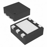
Available in a 2-mm × 2-mm 6-Pin SON Package
with 0.8-mm Height
The TPS60150 device operates in skip mode when
the load current falls less than 8 mA under typical
condition. In skip mode operation, quiescent current
is reduced to 90 μA.
Only 3 external capacitors are needed to generate
the output voltage, therefore saving PCB space.
Inrush current is limited by the soft-start function
during power on and power transient states.
The TPS60150 device operates over a free-air
temperature range of –40°C to 85°C. The device is
available with a small 2-mm × 2-mm 6-pin SON
package (QFN).
2 Applications
•
•
•
•
•
•
The 5-V output can supply a minimum of 140-mA
current.
USB On-the-Go (OTG)
HDMI
Portable Communication Devices
PCMCIA Cards
Mobile Phones, Smart Phones
Handheld Meters
Device Information(1)
PART NUMBER
PACKAGE
TPS60150
WSON (6)
BODY SIZE (NOM)
2.00 mm × 2.00 mm
(1) For all available packages, see the orderable addendum at
the end of the data sheet.
space
space
Typical Application Schematic
VIN
VOUT
(5.0V)
C3
2.2μF
C1
4.7μF
ENA
VIN
CP-
VOUT
CP+
100
ENABLE
/DISABLE
90
TA = 25°C
150 mA
80
C2
2.2μF
70
Efficiency - %
GND
Efficiency vs Input Voltage
120 mA
50 mA
100 mA
60
10 mA
50
40
30
20
10
0
2.7
3.2
3.7
4.2
4.7
VI - Input Voltage - V
5.2
1
An IMPORTANT NOTICE at the end of this data sheet addresses availability, warranty, changes, use in safety-critical applications,
intellectual property matters and other important disclaimers. PRODUCTION DATA.
�TPS60150
SLVS888C – DECEMBER 2008 – REVISED OCTOBER 2015
www.ti.com
Table of Contents
1
2
3
4
5
6
7
Features ..................................................................
Applications ...........................................................
Description .............................................................
Revision History.....................................................
Pin Configuration and Functions .........................
Specifications.........................................................
1
1
1
2
3
4
6.1
6.2
6.3
6.4
6.5
6.6
4
4
4
4
5
6
Absolute Maximum Ratings ......................................
ESD Ratings..............................................................
Recommended Operating Conditions.......................
Thermal Information ..................................................
Electrical Characteristics...........................................
Typical Characteristics ..............................................
Detailed Description .............................................. 7
7.1 Overview ................................................................... 7
7.2 Functional Block Diagram ......................................... 8
7.3 Feature Description................................................... 8
7.4 Device Functional Modes.......................................... 9
8
Application and Implementation ........................ 11
8.1 Application Information............................................ 11
8.2 Typical Application ................................................. 11
9 Power Supply Recommendations...................... 16
10 Layout................................................................... 16
10.1 Layout Guidelines ................................................. 16
10.2 Layout Example .................................................... 16
11 Device and Documentation Support ................. 17
11.1
11.2
11.3
11.4
Community Resources..........................................
Trademarks ...........................................................
Electrostatic Discharge Caution ............................
Glossary ................................................................
17
17
17
17
12 Mechanical, Packaging, and Orderable
Information ........................................................... 17
4 Revision History
NOTE: Page numbers for previous revisions may differ from page numbers in the current version.
Changes from Revision B (February 2011) to Revision C
•
Added Pin Configuration and Functions section, ESD Ratings table, Feature Description section, Device Functional
Modes, Application and Implementation section, Power Supply Recommendations section, Layout section, Device
and Documentation Support section, and Mechanical, Packaging, and Orderable Information section .............................. 1
Changes from Revision A (April 2009) to Revision B
•
2
Page
Page
Added the Thermal Table and deleted the Dissipation Rating Table..................................................................................... 4
Submit Documentation Feedback
Copyright © 2008–2015, Texas Instruments Incorporated
Product Folder Links: TPS60150
�TPS60150
www.ti.com
SLVS888C – DECEMBER 2008 – REVISED OCTOBER 2015
5 Pin Configuration and Functions
DRV Package
6-Pin WSON
Top View
GND
ENA
VIN
CP-
VOUT
CP+
Pin Functions
PIN
NAME
NO.
I/O
DESCRIPTION
CP+
4
—
Connect to the flying capacitor
CP–
5
—
Connect to the flying capacitor
ENA
6
IN
Hardware enable/disable pin (High = Enable)
GND
1
—
Ground
VIN
2
IN
Supply voltage input
VOUT
3
OUT
Output, connect to the output capacitor
Submit Documentation Feedback
Copyright © 2008–2015, Texas Instruments Incorporated
Product Folder Links: TPS60150
3
�TPS60150
SLVS888C – DECEMBER 2008 – REVISED OCTOBER 2015
www.ti.com
6 Specifications
6.1 Absolute Maximum Ratings
Over operating free-air temperature range (unless otherwise noted)
(1)
MIN
MAX
UNIT
VIN
Input voltage (all pins)
–0.3
7
V
TA
Operating temperature
–40
TJ
Maximum operating junction temperature
Tstg
Storage temperature
(1)
–55
85
°C
150
°C
150
°C
Stresses beyond those listed under Absolute Maximum Ratings may cause permanent damage to the device. These are stress ratings
only and functional operation of the device at these or any other conditions beyond those indicated under recommended operating
conditions is not implied. Exposure to absolute-maximum-rated conditions for extended periods may affect device reliability.
6.2 ESD Ratings
VALUE
V(ESD)
(1)
(2)
(3)
Electrostatic discharge
Human body model (HBM), per ANSI/ESDA/JEDEC JS-001 (1) (2)
±2000
Charged-device model (CDM), per JEDEC specification JESD22C101 (3)
±500
UNIT
V
JEDEC document JEP155 states that 500-V HBM allows safe manufacturing with a standard ESD control process.
The human body model (HBM) is a 100-pF capacitor discharged through a 1.5-kΩ resistor into each pin. The testing is done according
JEDECs EIA/JESD22-A114.
JEDEC document JEP157 states that 250-V CDM allows safe manufacturing with a standard ESD control process.
6.3 Recommended Operating Conditions
MIN
NOM
MAX
UNIT
VIN
Input voltage
2.7
5.5
V
TA
Operating ambient temperature
–40
85
°C
TJ
Operating junction temperature
–40
125
Cin
Input capacitor
2.2
μF
Co
Output capacitor
2.2
μF
Cf
Flying capacitor
1
μF
°C
6.4 Thermal Information
TPS60150
THERMAL METRIC (1)
DRV (WSON)
UNIT
6 PINS
RθJA
Junction-to-ambient thermal resistance
69.1
°C/W
RθJC(top)
Junction-to-case (top) thermal resistance
79.8
°C/W
RθJB
Junction-to-board thermal resistance
38.6
°C/W
ψJT
Junction-to-top characterization parameter
1.2
°C/W
ψJB
Junction-to-board characterization parameter
38.4
°C/W
RθJC(bot)
Junction-to-case (bottom) thermal resistance
9.2
°C/W
(1)
4
For more information about traditional and new thermal metrics, see the IC Package Thermal Metrics application report, SPRA953.
Submit Documentation Feedback
Copyright © 2008–2015, Texas Instruments Incorporated
Product Folder Links: TPS60150
�TPS60150
www.ti.com
SLVS888C – DECEMBER 2008 – REVISED OCTOBER 2015
6.5 Electrical Characteristics
VIN = 3.6 V, TA = –40°C to 85°C, typical values are at TA = 25°C, C1 = C3 = 2.2 μF, C2 = 1 μF (unless otherwise noted)
PARAMETER
TEST CONDITIONS
MIN
TYP
MAX
UNIT
POWER STAGE
VIN
Input voltage range
VUVLO
Undervoltage lockout threshold
IQ
Operating quiescent current
IOUT = 140 mA, Enable = VIN
4.7
mA
IQskip
Skip mode operating quiescent
current
IOUT = 0 mA, Enable=VIN (no switching)
80
μA
IOUT = 0 mA, Enable = VIN(minimum switching)
90
ISD
Shut down current
2.7 V ≤ VIN ≤ 5.5 V, Enable = 0 V
(1)
VOUT
Output voltage
VOUT(skip)
Skip mode output voltage
FSW
Switching frequency
SSTIME
Soft-start time
2.7
5.5
1.9
IOUT ≤ 50 mA, 2.7 V ≤ VIN < 5.5 V
4.8
IOUT = 0 mA, 2.7 V ≤ VIN ≤ 5.5 V
5
2.1
V
μA
1
μA
5.2
V
VOUT + 0.1
From the rising edge of enable to 90% output
V
V
1.5
MHz
150
μs
OUTPUT CURRENT
IOUT_nom
IOUT_short
Maximum output current
Short circuit current (2)
VOUT remains from 4.8 V to 5.2 V,
3.1 V ≤ VIN ≤ 5.5 V
120
3.3 V < VIN < 5.5 V
140
mA
VOUT = 0 V
80
mA
IOUT = 140 mA
30
mV
RIPPLE VOLTAGE
VR
Output ripple voltage
ENABLE CONTROL
VHI
Logic high input voltage
VLI
Logic low input voltage
IHI
ILI
2.7 V ≤ VIN ≤ 5.5 V
1.3
VIN
V
–0.2
0.4
V
Logic high input current
1
μA
Logic low input current
1
μA
THERMAL SHUTDOWN
TSD
Shutdown temperature
160
°C
TRC
Shutdown recovery
140
°C
(1)
(2)
When in skip mode, output voltage can exceed VOUT spec because VOUT(skip) = VOUT+0.1.
The TPS60150 device has internal protection circuit to protect IC when VOUT shorted to GND.
Submit Documentation Feedback
Copyright © 2008–2015, Texas Instruments Incorporated
Product Folder Links: TPS60150
5
�TPS60150
SLVS888C – DECEMBER 2008 – REVISED OCTOBER 2015
www.ti.com
6.6 Typical Characteristics
0.3
120
No load
No Switching
0.25
IO - Max Output Current - A
Input Current - µA
110
100
-85°C
90
80
25°C
-40°C
3.2
4.2
3.7
4.7
VI - Input Voltage - V
TA = 25°C
TA = 85°C
0.15
0.1
0
2.7
5.2
Figure 1. Quiescent Current vs Input Voltage
6
0.2
0.05
70
60
2.7
TA = -40°C
3.2
3.7
4.2
4.7
VI - Input Voltage - V
5.2
Figure 2. Maximum Output Current vs Input Voltage at
Temperature
Submit Documentation Feedback
Copyright © 2008–2015, Texas Instruments Incorporated
Product Folder Links: TPS60150
�TPS60150
www.ti.com
SLVS888C – DECEMBER 2008 – REVISED OCTOBER 2015
7 Detailed Description
7.1 Overview
The TPS60150 regulated charge pump provides a regulated output voltage for various input voltages. The
TPS60150 device regulates the voltage across the flying capacitor to 2.5 V and controls the voltage drop of Q1
and Q2 while a conversion clock with 50% duty cycle drives the FETs.
VIN
Q2
Q1
OFF
ON
2.5V
- +
Q3
CF
Q4
OFF
ON
VOUT
COUT
Figure 3. Charging Mode
During the first half cycle, Q2 and Q3 transistors are turned on and flying capacitor, CF, will be charged to 2.5 V
ideally.
VIN
Q1
Q2
OFF
VQ1
ON
2.5V
- +
Q3
OFF
CF
Q4
ON
VOUT
COUT
Figure 4. Discharging Mode
During the second half cycle, Q1 and Q4 transistors are turned on. Capacitor CF will then be discharged to
output.
Use Equation 1 to calculate the output voltage.
VOUT = VIN - VQ1 + V(CF) - VQ4 = VIN - VQ1 + 2.5 V - VQ4 = 5 V
(Ideal)
(1)
The output voltage is regulated by output feedback and an internally compensated voltage control loop.
Submit Documentation Feedback
Copyright © 2008–2015, Texas Instruments Incorporated
Product Folder Links: TPS60150
7
�TPS60150
SLVS888C – DECEMBER 2008 – REVISED OCTOBER 2015
www.ti.com
7.2 Functional Block Diagram
CF
CPTPS60150
VIN
CP+
5
4
2
TSD
UVLO
Regulation
Current Limit
Soft Start
Φ2
Φ1
Φ1
VREF
Bias circuit
Φ2
VOUT
3
ErrorAmp
Control
R1
+
-
ENA
6
Enable IC
OSC
1.5 MHz
R2
+
Skip Comp
1
GND
7.3 Feature Description
7.3.1 Enable
An enable pin on the regulator is used to place the device into an energy-saving shutdown mode. In this mode,
the output is disconnected from the input, and the input quiescent current is reduced to 10 μA maximum.
7.3.2 Undervoltage Lockout
When the input voltage drops, the undervoltage lockout prevents misoperation by switching off the device. The
converter starts operation again when the input voltage exceeds the threshold, provided the enable pin is high.
7.3.3 Thermal Shutdown Protection
The regulator has thermal shutdown circuitry that protects it from damage caused by overload conditions. The
thermal protection circuitry disables the output when the junction temperature reached approximately 160°C,
allowing the device to cool. When the junction temperature cools to approximately 140°C, the output circuitry is
automatically reenabled. Continuously running the regulator into thermal shutdown can degrade reliability. The
regulator also provides current limit to protect itself and the load.
8
Submit Documentation Feedback
Copyright © 2008–2015, Texas Instruments Incorporated
Product Folder Links: TPS60150
�TPS60150
www.ti.com
SLVS888C – DECEMBER 2008 – REVISED OCTOBER 2015
7.4 Device Functional Modes
7.4.1 Soft Start
An internal soft start limits the inrush current when the device is being enabled.
7.4.2 Normal Mode and Skip Mode Operation
The TPS60150 device has skip mode operation as shown in Figure 5. The TPS60150 device enters skip mode if
the output voltage reaches 5 V +0.1 V and the load current is less than 8 mA (typical). In skip mode, the
TPS60150 device disables the oscillator and decreases the prebias current of the output stage to reduce the
power consumption. Once the output voltage dips less than the threshold voltage of 5 V +0.1 V, the TPS60150
device begins switching to increase output voltage until the output reaches 5 V +0.1 V. When the output voltage
dips less than 5 V, the TPS60150 device returns to normal pulse width modulation (PWM) mode; thereby
reenabling the oscillator and increasing the prebias current of the output stage to supply output current.
The skip threshold voltage and current depend on input voltage and output current conditions.
4.7 mA
Quiescent Current
90 mA
50 mA
t
Load current
No load
t
VOUT
5 V +0.1 V
5V
t
Gate Waveform
Of Q1 Transistor
Start up
Waveform
t
Skip Mode at
Normal Mode at
Skip Mode at
No Load Condition 50 mA Load Current No Load Condition
Figure 5. Normal Mode and Skip Mode Operation
7.4.3 Short Circuit Protection
The TPS60150 device has internal short circuit protection to protect the IC when the output is shorted to ground.
To avoid damage when output is shorted to ground, the short circuit protection circuitry senses output voltage
and clamps the maximum output current to 80 mA (typical).
Submit Documentation Feedback
Copyright © 2008–2015, Texas Instruments Incorporated
Product Folder Links: TPS60150
9
�TPS60150
SLVS888C – DECEMBER 2008 – REVISED OCTOBER 2015
www.ti.com
Device Functional Modes (continued)
EN
VOUT
t
5.0V
4.5V
4.2V
Vout
t
Current Limit
300mA
IOUT_MAX
Output current
Output
Short circuit current
50mA(min)
t0
t1
t
t2
Soft Start
Vout is short to GND
Figure 6. Maximum Output Current Capability and Short Circuit Protection
10
Submit Documentation Feedback
Copyright © 2008–2015, Texas Instruments Incorporated
Product Folder Links: TPS60150
�TPS60150
www.ti.com
SLVS888C – DECEMBER 2008 – REVISED OCTOBER 2015
8 Application and Implementation
NOTE
Information in the following applications sections is not part of the TI component
specification, and TI does not warrant its accuracy or completeness. TI’s customers are
responsible for determining suitability of components for their purposes. Customers should
validate and test their design implementation to confirm system functionality.
8.1 Application Information
Most of today’s battery-powered portable electronics allow and/or require data transfer with a PC. One of the
fastest data transfer protocols is through USB On-the-Go (OTG). As Figure 7 shows, the USB OTG circuitry in
the portable device requires a 5-V power rail and up to 140 mA of current. The TPS60150 device may be used to
provide a 5-V power rail in a battery powered system.
8.2 Typical Application
8.2.1 USB On the Go Circuitry
GND
ENA
VIN
CP-
VOUT
CP+
VIN = 2.7 V - 5.5 V
140mA (VIN > 3.3V)
50mA (VIN > 2.7V)
C2
1 mF
C3
C1
2.2 mF 2.2 mF
5V
Controller
VBUS
GND
ID
USB
Transceiver
D+
Comparator
D-
Figure 7. Application Circuit for OTG System
8.2.1.1 Design Requirements
The design guideline provides a component selection to operate the device within the Recommended Operating
Conditions.
8.2.1.2 Detailed Design Procedure
8.2.1.2.1 Capacitor Selection
For minimum output voltage ripple, the output capacitor (COUT) should be a surface-mount ceramic capacitor.
Tantalum capacitors generally have a higher effective series resistance (ESR) and may contribute to higher
output voltage ripple. Leaded capacitors also increase ripple due to the higher inductance of the package itself.
To achieve the best operation with low input voltage and high load current, the input and flying capacitors (CIN
and CF, respectively) should also be surface-mount ceramic types.
Submit Documentation Feedback
Copyright © 2008–2015, Texas Instruments Incorporated
Product Folder Links: TPS60150
11
�TPS60150
SLVS888C – DECEMBER 2008 – REVISED OCTOBER 2015
www.ti.com
Typical Application (continued)
VIN
VOUT
(5 V)
GND
ENA
VIN
CP-
VOUT
COUT
ENABLE
/DISABLE
CF
CP+
CIN
Figure 8. Capacitors
Generally, CFLY can be calculated using Equation 2.
Qcharging = c ´ v = CFLY ´ D VCFLY ,
æT ö
Qdischarging = idischarge ´ t = 2 ´ ILO AD(MAX) ´ ç ÷ , half duty.
è2ø
(2)
æTö
\ 2 ´ ILOAD(MAX) ´ ç ÷ = CFLY ´ DVCFLY
è 2ø
Both equation should be same,
\ CFLY
æTö
2 ´ ILOAD(MAX) ´ ç ÷
è 2 ø = ILOAD(MAX)
³
DVCFLY
DVCFLY ´ ¦
(3)
If ILOAD = 140 mA, f = 1.5 MHZ, and ΔVCFLY = 100 mV, the minimum value of the flying capacitor should be 1 μF.
Output capacitance, COUT, is also strongly related to output ripple voltage and loop stability,
ILOAD(MAX)
+ 2I
´ ESRCOUT
VOUT(RIPPLE) =
(2 ´ f ´ COUT ) LOAD(MAX)
(4)
The minimum output capacitance for all output levels is 2.2 μF due to control stability. Larger ceramic capacitors
or low ESR capacitors can be used to lower the output ripple voltage.
Table 1. Suggested Capacitors (Input, Output, and Flying Capacitor)
VALUE
DIELECTRIC MATERIAL
PACKAGE SIZE
RATED VOLTAGE
4.7 μF
X5R or X7R
0603
10 V
2.2 μF
X5R or X7R
0603
10 V
The efficiency of the charge pump regulator varies with the output voltage, the applied input voltage and the load
current.
Use Equation 5 and Equation 6 to calculate the approximate efficiency in normal operating mode is given by:
´ IOUT
V
PD(out)
´ 100 = OUT
´ 100 , IIN = 2 ´ IOUT + IQ
Efficiency(%) =
PD(in)
VIN ´ IIN
(5)
VOUT
Efficiency(%) =
× 100 (IIN = 2 ´ IOUT ) Quiescent current was neglected.
2 × VIN
(6)
12
Submit Documentation Feedback
Copyright © 2008–2015, Texas Instruments Incorporated
Product Folder Links: TPS60150
�TPS60150
www.ti.com
SLVS888C – DECEMBER 2008 – REVISED OCTOBER 2015
8.2.1.3 Application Curves
5.10
5.25
TA = 25°C
TA = 25°C
5.2
5.05
10 mA
VO - Output Voltage - V
VO - Output Voltage - V
5.15
5.1
5.05
3.6 V
4.2 V
5V
5.5 V
5
4.95
50 mA
5.00
150 mA
4.95
120 mA
4.90
100 mA
4.85
4.9
2.7 V
4.85
0
0.05
0.1
0.15
IO - Output Current - A
0.2
Figure 9. Output Voltage vs Output Current
4.80
2.7
3.2
3.7
4.2
4.7
VI - Input Voltage - V
5.2
Figure 10. Output Voltage vs Input Voltage
100
TA = 25°C
90
150 mA
80
120 mA
50 mA
Efficiency - %
70
100 mA
60
10 mA
50
40
30
20
10
0
2.7
3.2
3.7
4.2
4.7
VI - Input Voltage - V
5.2
20 ms/div
Figure 11. Efficiency vs Input Voltage
20 ms/div
Figure 13. Load Transient Response
VIN = 3.6 V, IO = 60 mA to 100 mA
Figure 12. Load Transient Response
VIN = 2.7 V, IO = 30 mA to 50 mA
5 ms/div
Figure 14. Output Ripple Voltage (Skip Mode)
VIN = 2.7 V, IO = 0 mA
Submit Documentation Feedback
Copyright © 2008–2015, Texas Instruments Incorporated
Product Folder Links: TPS60150
13
�TPS60150
SLVS888C – DECEMBER 2008 – REVISED OCTOBER 2015
14
www.ti.com
5 ms/div
Figure 15. Output Ripple Voltage (Skip Mode)
VIN = 3.6 V, IO = 0 mA
500 ns/div
Figure 16. Output Ripple Voltage (Normal Mode)
VIN = 2.7 V, IO = 50 mA
500 ns/div
Figure 17. Output Ripple (Normal Mode)
VIN = 3.6 V, IO = 100 mA
1 ms/div
Figure 18. Power On
VIN = 2.7 V, IO = 50 mA
1 ms/div
Figure 19. Power On
VIN = 3.6 V, IO = 100 mA
Figure 20. Enable / Disable
VIN = 2.7 V, IO = 50 mA
200 ms/div
Submit Documentation Feedback
Copyright © 2008–2015, Texas Instruments Incorporated
Product Folder Links: TPS60150
�TPS60150
www.ti.com
SLVS888C – DECEMBER 2008 – REVISED OCTOBER 2015
200 ms/div
50 ms/div
Figure 22. Thermal Shutdown Operation
VIN = 5.5 V, RLOAD= 20 Ω
Figure 21. Enable / Disable
VIN = 3.6 V, IO = 100 mA
8.2.2 System Example
Low-cost portable electronics with small LCD displays require a low-cost solution for providing the WLED
backlight. As shown in Figure 23, the TPS60150 device can also be used to drive several WLEDs in parallel, with
the help of ballast resistors.
VIN = 2.7 V~5.5 V
140mA (VIN > 3.3V)
GND
ENA
VIN
CP-
VOUT
CP+
ENABLE
C2
1 mF
50mA (VIN > 2.7V)
C3
C1
2.2 mF 2.2 mF
Figure 23. Application Circuit for Driving White LEDs
Submit Documentation Feedback
Copyright © 2008–2015, Texas Instruments Incorporated
Product Folder Links: TPS60150
15
�TPS60150
SLVS888C – DECEMBER 2008 – REVISED OCTOBER 2015
www.ti.com
9 Power Supply Recommendations
The TPS60150 device has no special requirements for its input power supply. The input power supply's output
current must be rated according to the supply voltage, output voltage and output current of the TPS60150
device.
10 Layout
10.1 Layout Guidelines
Large transient currents flow in the VIN, VOUT, and GND traces. To minimize both input and output ripple, keep
the capacitors as close as possible to the regulator using short, direct circuit traces.
10.2 Layout Example
GND
VIN
GND
VOUT
Figure 24. Recommended PCB Layout
16
Submit Documentation Feedback
Copyright © 2008–2015, Texas Instruments Incorporated
Product Folder Links: TPS60150
�TPS60150
www.ti.com
SLVS888C – DECEMBER 2008 – REVISED OCTOBER 2015
11 Device and Documentation Support
11.1 Community Resources
The following links connect to TI community resources. Linked contents are provided "AS IS" by the respective
contributors. They do not constitute TI specifications and do not necessarily reflect TI's views; see TI's Terms of
Use.
TI E2E™ Online Community TI's Engineer-to-Engineer (E2E) Community. Created to foster collaboration
among engineers. At e2e.ti.com, you can ask questions, share knowledge, explore ideas and help
solve problems with fellow engineers.
Design Support TI's Design Support Quickly find helpful E2E forums along with design support tools and
contact information for technical support.
11.2 Trademarks
E2E is a trademark of Texas Instruments.
All other trademarks are the property of their respective owners.
11.3 Electrostatic Discharge Caution
These devices have limited built-in ESD protection. The leads should be shorted together or the device placed in conductive foam
during storage or handling to prevent electrostatic damage to the MOS gates.
11.4 Glossary
SLYZ022 — TI Glossary.
This glossary lists and explains terms, acronyms, and definitions.
12 Mechanical, Packaging, and Orderable Information
The following pages include mechanical, packaging, and orderable information. This information is the most
current data available for the designated devices. This data is subject to change without notice and revision of
this document. For browser-based versions of this data sheet, refer to the left-hand navigation.
Submit Documentation Feedback
Copyright © 2008–2015, Texas Instruments Incorporated
Product Folder Links: TPS60150
17
�PACKAGE OPTION ADDENDUM
www.ti.com
10-Dec-2020
PACKAGING INFORMATION
Orderable Device
Status
(1)
Package Type Package Pins Package
Drawing
Qty
Eco Plan
(2)
Lead finish/
Ball material
MSL Peak Temp
Op Temp (°C)
Device Marking
(3)
(4/5)
(6)
TPS60150DRVR
ACTIVE
WSON
DRV
6
3000
RoHS & Green NIPDAU | NIPDAUAG
Level-1-260C-UNLIM
-40 to 85
CGO
TPS60150DRVT
ACTIVE
WSON
DRV
6
250
RoHS & Green NIPDAU | NIPDAUAG
Level-1-260C-UNLIM
-40 to 85
CGO
(1)
The marketing status values are defined as follows:
ACTIVE: Product device recommended for new designs.
LIFEBUY: TI has announced that the device will be discontinued, and a lifetime-buy period is in effect.
NRND: Not recommended for new designs. Device is in production to support existing customers, but TI does not recommend using this part in a new design.
PREVIEW: Device has been announced but is not in production. Samples may or may not be available.
OBSOLETE: TI has discontinued the production of the device.
(2)
RoHS: TI defines "RoHS" to mean semiconductor products that are compliant with the current EU RoHS requirements for all 10 RoHS substances, including the requirement that RoHS substance
do not exceed 0.1% by weight in homogeneous materials. Where designed to be soldered at high temperatures, "RoHS" products are suitable for use in specified lead-free processes. TI may
reference these types of products as "Pb-Free".
RoHS Exempt: TI defines "RoHS Exempt" to mean products that contain lead but are compliant with EU RoHS pursuant to a specific EU RoHS exemption.
Green: TI defines "Green" to mean the content of Chlorine (Cl) and Bromine (Br) based flame retardants meet JS709B low halogen requirements of